

®
EL2480
Data Sheet May 23, 2005
250MHz/3mA Current Mode Feedback
Amplifier
The EL2480 is a quad current-feedback operational amplifier
which achieves a -3dB bandwidth of 250MHz at a gain of +1
while consuming only 3mA of supply current per amplifier. It
will operate with dual supplies ranging from ±1.5V to ±6V, or
from single supplies ranging from +3V to +12V. In spite of its
low supply current, the EL2480 can output 55mA while
swinging to ±4V on ±5V supplies. These attributes make the
EL2480 an excellent choice for low po wer and/or lo w v oltage
cable-driver, HDSL, or RGB applications.
For triple applications with disable, consider the EL2386 (16pin triple).
Ordering Information
PKG.
PART NUMBER PACKAGE TAPE & REEL
EL2480CS 14-Pin SO - MDP0027
EL2480CS-T7 14-Pin SO 7” MDP0027
EL2480CS-T13 14-Pin SO 13” MDP0027
EL2480CSZ
(See Note)
EL2480CSZ-T7
(See Note)
EL2480CSZ-T13
(See Note)
NOTE: Intersil Pb-free products employ special Pb-free material sets;
molding compounds/die attach materials and 100% matte tin plate
termination finish, which are RoHS compliant and compatible with
both SnPb and Pb-free soldering operations. Intersil Pb-free products
are MSL classified at Pb-free peak reflow temperatures that meet or
exceed the Pb-free requirements of IPC/JEDEC J STD-020.
14-Pin SO
(Pb-free)
14-Pin SO
(Pb-free)
14-Pin SO
(Pb-free)
- MDP0027
7” MDP0027
13” MDP0027
DWG. #
FN7055.1
Features
• Quad topology
• 3mA supply current (per amplifier)
• 250MHz -3dB bandwidth
• Low cost
• Single- and dual-supply operation down to ±1.5V
• 0.05%/0.05° diff. gain/diff. phase into 150Ω
• 1200V/µs slew rate
• Large output drive current - 55mA
• Also available with disable in triple
• Pb-Free plus Anneal available (RoHS compliant)
Applications
• Low power/battery applications
• HDSL amplifiers
• Video amplifiers
• Cable drivers
• RGB amplifiers
• Test equipment amplifiers
• Current to voltage converters
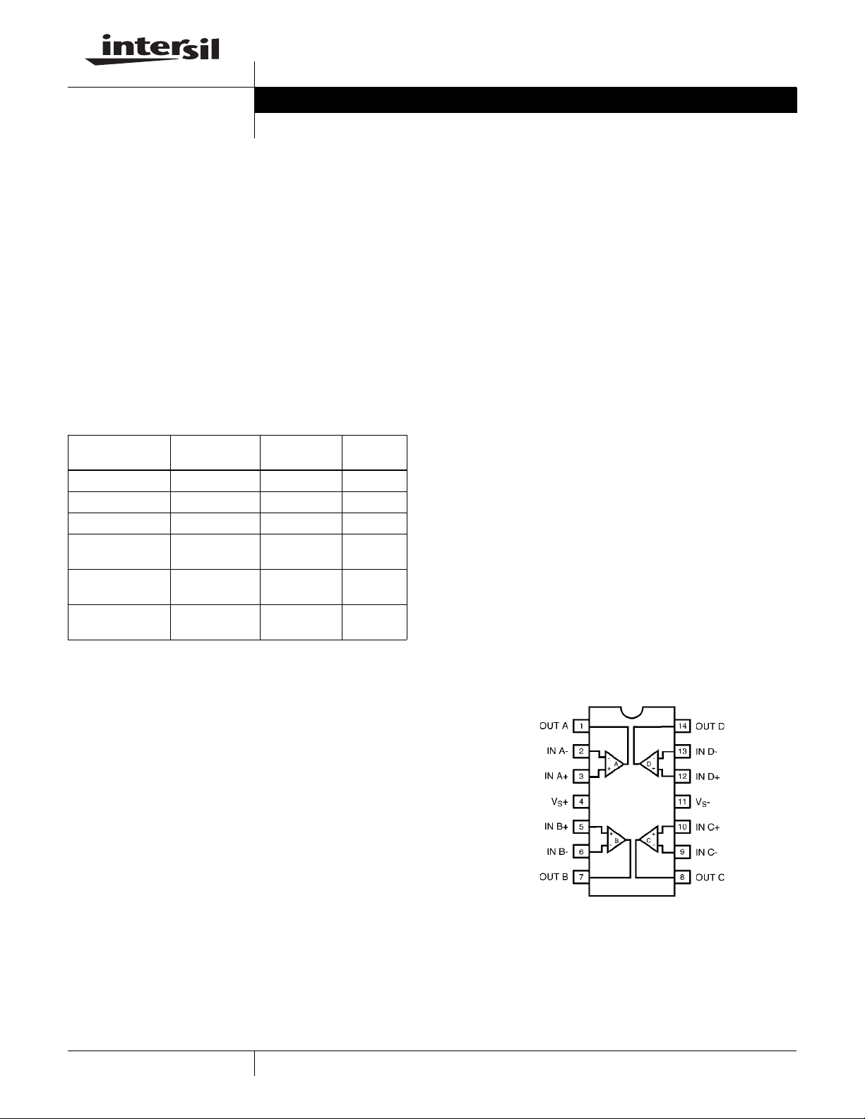
Pinout
EL2480
(14-PIN SO)
TOP VIEW
1
CAUTION: These devices are sensitive to electrostatic discharge; follow proper IC Handling Procedures.
1-888-INTERSIL or 1-888-352-6832
| Intersil (and design) is a registered trademark of Intersil Americas Inc.
Copyright Intersil Americas Inc. 2002, 2003, 2005. All Rights Reserved
All other trademarks mentioned are the property of their respective owners.
EL2480
Absolute Maximum Ratings (T
Supply Voltage between V
Voltage between V
Common-Mode Input Voltage . . . . . . . . . . . . . . . . . . . . . V
S
Differential Input Voltage . . . . . . . . . . . . . . . . . . . . . . . . . . . . . . . ±6V
Current into +IN or -IN . . . . . . . . . . . . . . . . . . . . . . . . . . . . . .±7.5mA
+ and GND. . . . . . . . . . . . . . . . . +12.6V
S
+ and VS-. . . . . . . . . . . . . . . . . . . . . . . . +12.6V
= 25°C)
A
- to VS+
S
Internal Power Dissipation. . . . . . . . . . . . . . . . . . . . . . . See Curves
Operating Ambient Temperature Range . . . . . . . . . .-40°C to +85°C
Operating Junction Temperature
Plastic Packages . . . . . . . . . . . . . . . . . . . . . . . . . . . . . . . . . . .150°C
Output Current. . . . . . . . . . . . . . . . . . . . . . . . . . . . . . . . . . . . ±60mA
Storage Temperature Range . . . . . . . . . . . . . . . . . .-65°C to +150°C
CAUTION: Stresses above those listed in “Absolute Maximum Ratings” may cause permanent damage to the device. This is a stress only rating and operation of the
device at these or any other conditions above those indicated in the operational sections of this specification is not implied.
IMPORTANT NOTE: All parameters having Min/Max specifications are guaranteed. Typical values are for information purposes only. Unless otherwise noted, all tests
are at the specified temperature and are pulsed tests , therefore: TJ = TC = T
DC Electrical Specifications V
= ±5V, RL = 150Ω, TA = 25°C unless otherwise specified
S
A
PARAMETER DESCRIPTION CONDITIONS MIN TYP MAX UNIT
V
OS
TCV
dV
+I
IN
d+I
-I
IN
d-I
OS
OS
IN
IN
Input Offset Voltage 2.5 10 mV
Average Input Offset Voltage Drift Measured from T
MIN
to T
MAX
5µV/°C
VOS Matching 0.5 mV
+Input Current 1.5 15 µA
+IIN Matching 20 nA
-Input Current 16 40 µA
-IIN Matching 2µA
CMRR Common Mode Rejection Ratio VCM = ±3.5V 45 50 dB
-ICMR -Input Current Common Mode
V
= ±3.5V 5 30 µA/V
CM
Rejection
PSRR Power Supply Rejection Ratio V
-IPSR - Input Current Power Supply
is moved from ±4V to ±6V 60 70 dB
S
V
is moved from ±4V to ±6V 1 15 µA/V
S
Rejection
R
+R
+C
OL
IN
IN
Transimpedance V
= ±2.5V 120 300 kΩ
OUT
+Input Resistance VCM = ±3.5V 0.5 2 MΩ
+Input Capacitance 1.2 pF
CMIR Common Mode Input Range ±3.5 ±4.0 V
V
O
Output Voltage Swing VS = ±5 ±3.5 ±4.0 V
V
= 5 single-supply, high 4.0 V
S
VS = 5 single-supply, low 0.3 V
I
O
I
S
Output Current
Per amplifier 50 55 mA
Supply Current Per amplifier 3 6 mA
2
EL2480
AC Electrical Specifications V
=±5V, RF=RG= 750Ω, RL=150Ω, TA= 25°C unless otherwise specified
S
PARAMETER DESCRIPTION CONDITIONS MIN TYP MAX UNIT
-3dB BW -3dB Bandwidth A
= 1 250 MHz
V
-3dB BW -3dB Bandwidth AV = 2 180 MHz
0.1dB BW 0.1dB Bandwidth A
SR Slew Rate V
tR, t
t
PD
F
Rise and Fall Time V
Propagation Delay V
OS Overshoot V
t
S
0.1% Settling V
dG Differential Gain A
dP Differential Phase A
= 2 50 MHz
V
= ±2.5V, AV = 2 600 1200 V/µs
OUT
= ±500mV 1.5 ns
OUT
= ±500mV 1.5 ns
OUT
= ±500mV 3.0 %
OUT
= ±2.5V, AV = -1 15 ns
OUT
= 2, RL = 150Ω (Note 1) 0.05 %
V
= 2, RL = 150Ω (Note 1) 0.05 °
V
dG Differential Gain AV = 1, RL = 500Ω (Note 1) 0.01 %
dP Differential Phase A
C
S
Channel Separation f = 5MHz 85 dB
= 1, RL = 500Ω (Note 1) 0.01 °
V
NOTE:
1. DC offset from 0V to 0.714V, AC amplitude 286mV
, f = 3.58MHz
P-P
3
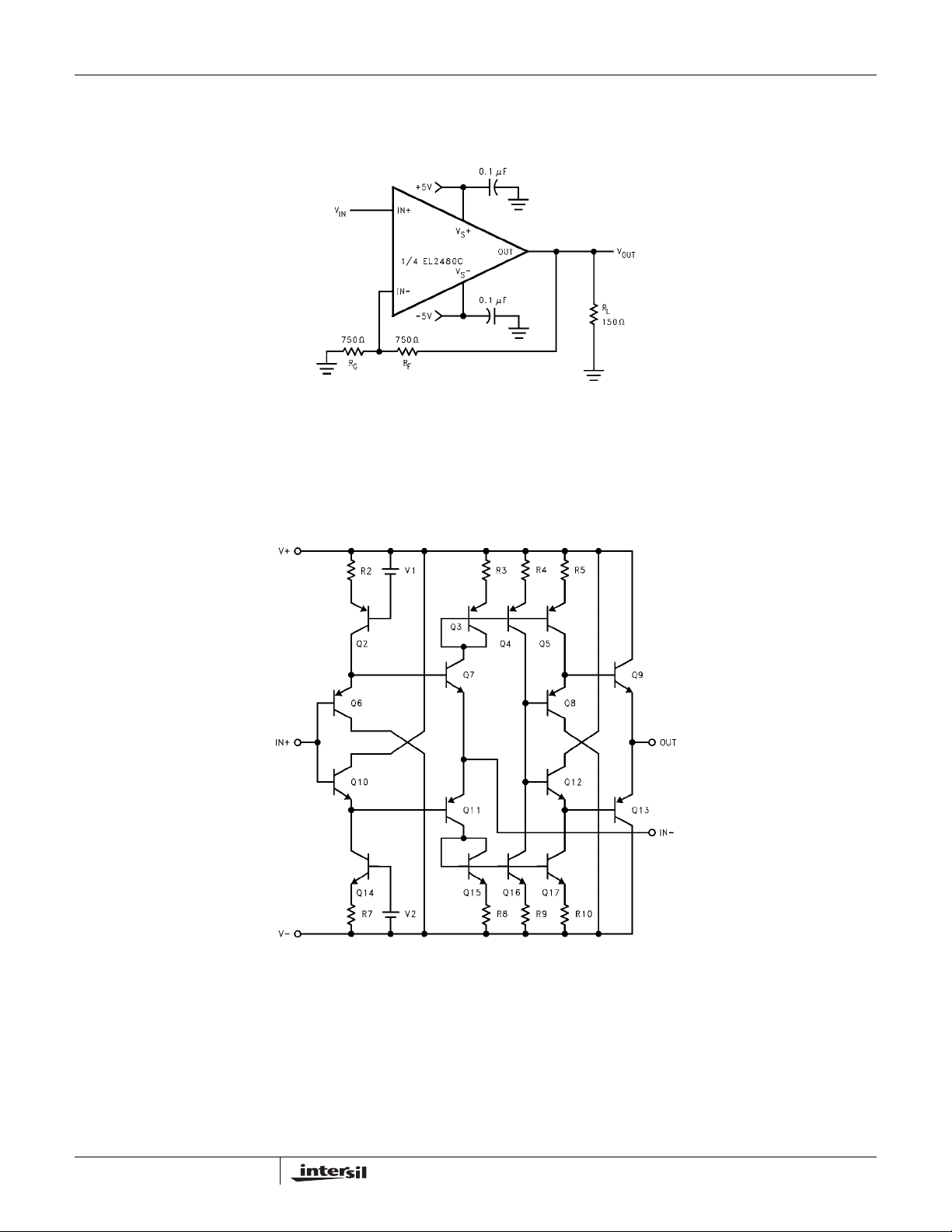
Test Circuit (per Amplifier)
Simplified Schematic (per Amplifier)
EL2480
4

Typical Performance Curves
EL2480
Non-Inverting Frequency
Response (Gain)
Inverting Frequency
Response (Gain)
Ω
Non–Inverting Frequency
Response (Phase)
Inverting Frequency
Response (Phase)
Frequency Response
for Various RF and R
Frequency Response
for Various RL and C
G
L
Transimpedance (ROL) vs
Frequency
PSRR and CMRR
vs Frequency
Frequency Response for
Various CIN-
5

Typical Performance Curves (Continued)
EL2480
Voltage and Current
Noise vs Frequency
-3dB Bandwidth and Peaking
vs Supply Voltage for
Various Non-Inverting Gains
2nd and 3rd Harmonic
Distortion vs Frequency
-3dB Bandwidth and Peaking
vs Supply Voltage for
Various Inverting Gains
Output Voltage
Swing vs Frequency
Output Voltage Swing
vs Supply Voltage
Supply Current vs Supply Voltage
Common-Mode Input Range
vs Supply Voltage
Slew Rate vs Supply Voltage
6

Typical Performance Curves (Continued)
EL2480
Input Bias Current
vs Die Temperature
-3dB Bandwidth and Peaking
vs Die Temperature for
Various Non-Inverting Gains
Short-Circuit Current
vs Die Temperature
-3dB Bandwidth vs
Die Temperature for
Various Inverting Gains
Transimpedance (ROL)
vs Die Temperature
Input Offset Voltage
vs Die Temperature
Supply Current vs Die Temperature
Input Voltage Range
vs Die Temperature
Slew Rate vs Die Temperature
7

Typical Performance Curves (Continued)
EL2480
Differential Gain and
Phase vs DC Input
Voltage at 3.58MHz
Differential Gain and
Phase vs DC Input
Voltage at 3.58MHz
Channel Separation
vs Frequency
Settling Time vs
Settling Accuracy
Small-Signal Step Response
JEDEC JESD51-7 HIGH EFFECTIVE
THERMAL CONDUCTIVITY TEST BOARD
1.8
1.6
1.420W
1.4
1.2
1
0.8
0.6
0.4
POWER DISSIPATION (W)
0.2
0
0 25 50 75 100 150
AMBIENT TEMPERATURE (°C)
SO14
θJA=88°C/W
Large-Signal Step Response
JEDEC JESD51-3 LOW EFFECTIVE
THERMAL CONDUCTIVITY TEST BOARD
1.2
1.042W
1
0.8
0.6
0.4
0.2
POWER DISSIPATION (W)
0
12585
0 25 50 75 100 150
AMBIENT TEMPERATURE (°C)
SO14
θJA=120°C/W
12585
8

EL2480
Applications Information
Product Description
The EL2480 is a current-feedback operational amplifier that
offers a wide -3dB bandwidth of 250MHz and a low supply
current of 3mA per amplifier. This product also features high
output current drive. The EL2480 can output 55mA per
amplifier. The EL2480 works with supply voltages ranging
from a single 3V to ±6V , and it is also capable of swinging to
within 1V of either supply on the input and the output.
Because of its current-feedback topology, the EL2480 does
not have the normal gain-bandwidth product associated with
voltage-feedback operational amplifiers. This allows its -3dB
bandwidth to remain relatively constant as closed-loop gain
is increased. This combination of high bandwidth and low
power, together with aggressive pricing make the EL2480
the ideal choice for many low-power/high-bandwidth
applications such as portable computing, HDSL, and video
processing.
The EL2480 is available in the industry standard SO
package. For triple application with disable, consider the
EL2386 (16-pin triple).
Power Supply Bypassing and Printed Circuit
Board Layout
As with any high-frequency device, good printed circuit
board layout is necessary for optimum performance. Ground
plane construction is highly recommended. Lead lengths
should be as short as possible. The power supply pins must
be well bypassed to reduce the risk of oscillation. The
combination of a 4.7µF tantalum capacitor in parallel with a
0.1µF capacitor has been shown to work well when placed at
each supply pin.
For good AC performance, parasitic capacitance sh ould be
kept to a minimum especially at the inverting input (see the
Capacitance at the Inverting Input section). Ground plane
construction should be used, but it should be removed from
the area near the inverting input to minimize any stray
capacitance at that node. Carbon or Metal-Film resistors are
acceptable with the Metal-Film resistors giving slightly less
peaking and bandwidth because of their additional series
inductance. Use of sockets, should be avoided if possible.
Sockets add parasitic inductance and capacitance which will
result in some additional peaking and overshoot.
Capacitance at the Inverting Input
Any manufacturer's high-speed voltage- or current-feedback
amplifier can be affected by stray capacitance at the
inverting input. For inverting gains this parasitic capacitance
has little effect because the inverting input is a virtual
ground, but for non-inverting gains this capacitance (in
conjunction with the feedback and gain resistors) creates a
pole in the feedback path of the amplifier. This pole, if low
enough in frequency, has the same destabilizing effect as a
zero in the forward open-loop response. The use of large
value feedback and gain resistors further exacerbates the
problem by further lowering the pole frequency.
The experienced user with a large amount of PC board
layout experience may find in rare cases that the EL2480
has less bandwidth than expected.
The reduction of feedback resistor values (or the addition of
a very small amount of external capacitance at the inverting
input, e.g. 0.5pF) will increase bandwidth as desired. Please
see the curves for Frequency Response for Various R
R
, and Frequency Response for Various CIN-.
G
and
F
Feedback Resistor Values
The EL2480 has been designed and specified at gains of +1
and +2 with R
give 250MHz of -3dB bandwidth at A
of peaking, and 180MHz of -3dB bandwidth at A
about 0.1dB of peaking. Since the EL2480 is currentfeedback amplifier, it is also possible to change the value of
R
to get more bandwidth. As seen in the curve of
F
Frequency Response For Various R
and peaking can be easily modified by varying the value of
the feedback resistor.
Because the EL2480 is current-feedback amplifier, its gainbandwidth product is not a constant for different closed-loop
gains. This feature actually allows the EL2480 to maintain
about the same -3dB bandwidth, regardless of closed-loop
gain. However, as closed-loop gain is increased, bandwidth
decreases slightly while stability increases. Since the loop
stability is improving with higher closed-loop gains, it
becomes possible to reduce the value of R
specified 560Ω and 750Ω and still retain stability, resulting in
only a slight loss of bandwidth with increased closed-loop
gain.
= 750Ω. These values of feedback resistors
F
= +1 with about 2.5dB
V
and RG, bandwidth
F
= +2 with
V
below the
F
Supply Voltage Range and Single-Supply
Operation
The EL2480 has been designed to operate with supply
voltages having a span of greater than 3V, and less than
12V. In practical terms, this means that the EL2480 will
operate on dual supplies ranging from ±1.5V to ±6V. With a
single-supply, the EL2480 will operate from +3V to +12V.
As supply voltages continue to decrease, it becomes
necessary to provide input and output voltage ranges that
can get as close as possible to the supply voltages. The
EL2480 has an input voltage range that extends to within 1V
of either supply . So, for example, on a single +5V supply, the
EL2480 has an input range which spans from 1V to 4V. The
output range of the EL2480 is also quite large, extending to
within 1V of the supply rail. On a ±5V suppl y, the output is
therefore capable of swinging from -4V to +4V. Single-supply
output range is even larger because of the increased
negative swing due to the external pull-down resistor to
ground. On a single +5V supply, output voltage range is
about 0.3V to 4V.
9

EL2480
Video Performance
For good video performance, an amplifier is required to
maintain the same output impedance and the same
frequency response as DC levels are changed at the output.
This is especially difficult when driving a standard video load
of 150Ω, because of the change in output current with DC
level. Until the EL2480, good Differential Gain could only be
achieved by running high idle currents through the output
transistors (to reduce variations in output impedance). These
currents were typically comparable to the entire 3mA supply
current of EL2480 amplifier! Special circuitry has been
incorporated in the EL2480 to reduce the variation of output
impedance with current output. This results in dG and dP
specifications of 0.05% and 0.05° while driving 150Ω at a
gain of +2.
Video performance has also been measured with a 500Ω
load at a gain of +1. Under these conditions, the EL2480 has
dG and dP specifications of 0.01% and 0.01° respectively
while driving 500Ω at A
= +1.
V
Output Drive Capability
This amplifier of the EL2480 is capable of providing a
minimum of ±50mA. These output drive levels are
unprecedented in amplifiers running at these supply currents.
The ±50mA minimum output drive of the EL2480 amplifier
allows swings of ±2.5V into 50Ω loads .
modified for the EL2480 to remain in the safe oper ating are a.
These parameters are calculated as follo ws:
T
JMAXTMAXΘJA
nPD
××()+=
MAX
where:
T
= Maximum ambient temperature
MAX
θ
= Thermal resistance of the package
JA
n = Number of amplifiers in the package
PD
= Maximum power dissipation of each amplifier in
MAX
the package
PD
for each amplifier can be calculated as follo ws:
PD
MAX
MAX
2( VSI
SMAX
) VS( - V
OUTMAX
V
OUTMAX
----------------------------
)
×+××=
R
L
where:
= Supply voltage
V
S
I
= Maximum supply current of 1 amplifier
SMAX
V
OUTMAX
R
L
= Maximum output voltage of the application
= Load resistance
Driving Cables and Capacitive Loads
When used as a cable driver, double termination is always
recommended for reflection-free perf ormance. For those
applications, the back-termination series resistor will decouple
the EL2480 from the cable and allow e x tensive capacitive
drive. However, other applicatio ns may have high capacitiv e
loads without a back-termination resistor . In these
applications, a small series resistor (usually between 5Ω and
50Ω) can be placed in series with the output to eliminate most
peaking. The gain resistor (R
) can then be chosen to make
G
up for any gain loss which may be created by this additional
resistor at the output. In many cases it is also possible to
simply increase the value of the f eedback resistor (R
F
) to
reduce the peaking.
Current Limiting
The EL2480 has no internal current-limiting circuitry. If any
output is shorted, it is possible to exceed the Absolute
Maximum Ratings for output current or powe r dissipatio n,
potentially resulting in the destruction of the device.
Power Dissipation
With the high output drive capability of the EL2480, it is
possible to ex ceed the 150 °C Absolute Maximu m j unction
temperature under certain very high load current conditions.
Generally speaking, when R
important to calculate the maximum junction temperature
(T
) for the application to determine if power-supply
JMAX
voltages, load conditions, or package type need to be
falls below about 25Ω, it is
L
10

Typical Application Circuits
EL2480
EL2480
EL2480
INVERTING 200mA OUTPUT CURRENT DISTRIBUTION
AMPLIFIER
FAST-SETTLING PRECISION AMPLIFIER
120
120
11
DIFFERENTIAL LINE-DRIVER/RECEIVER

EL2480 Macromodel
* EL2480 Macromodel
* Revision A, March 1995
* AC characteristics used: Rf = Rg = 750Ω
* Connections: +input
* | -input
* | | +Vsupply
* | | | -Vsupply
* | | | | output
* | | | | |
.subckt EL2480/el 3 2 4 11 1
*
* Input Stage
*
e1 10 0 3 0 1.0
vis 10 9 0V
h2 9 12 vxx 1.0
r1 2 11 400
l1 11 12 25nH
iinp 3 0 1.5uA
iinm 2 0 3uA
r12 3 0 2Meg
*
* Slew Rate Limiting
*
h1 13 0 vis 600
r2 13 14 1K
d1 14 0 dclamp
d2 0 14 dclamp
*
* High Frequency Pole
*
e2 30 0 14 0 0.00166666666
l3 30 17 150nH
c5 17 0 0.8pF
r5 17 0 165
*
* Transimpedance Stage
*
g1 0 18 17 0 1.0
rol 18 0 450K
cdp 18 0 0.675pF
*
* Output Stage
*
q1 11 18 19 qp
q2 4 18 20 qn
q3 4 19 21 qn
q4 11 20 22 qp
r7 21 1 4
r8 22 1 4
ios1 4 19 1mA
ios2 20 11 1mA
*
* Supply Current
*
ips 4 11 0.2mA
*
* Error Terms
EL2480
12

*
ivos 0 23 0.2mA
vxx 23 0 0V
e4 24 0 3 0 1.0
e5 25 0 4 0 1.0
e6 26 0 11 0 -1.0
r9 24 23 316
r10 25 23 3.2K
r11 26 23 3.2K
*
* Models
*
.model qn npn(is=5e-15 bf=200 tf=0.01nS)
*.model qp pnp(is=5e-15 bf=200 tf=0.01nS)
.model dclamp d(is=1e-30 ibv=0.266
+ bv=0.71v n=4)
.ends
EL2480 Macromodel
EL2480
4
1
11
All Intersil U.S. products are manufactured, assembled and tested utilizing ISO9000 quality systems.
Intersil Corporation’s quality certifications can be viewed at www.intersil.com/design/quality
Intersil products are sold by description only. Intersil Corporation reserves the right to make changes in circuit design, software and/or specifications at any time without
notice. Accordingly, the reader is cautioned to verify that data sheets are current before placing orders. Information furnished by Intersil is believed to be accurate and
reliable. However, no responsibility is assumed by Intersil or its subsidiaries for its use; nor for any infringements of patents or other rights of third parties which may result
from its use. No license is granted by implication or otherwise under any patent or patent rights of In tersi l or its subsidi aries.
For information regarding Intersil Corporation and its products, see www.intersil.com
13
 Loading...