

Page 1
®
EL2126
FN7046.4Data Sheet May 2, 2007
Ultra-Low Noise, Low Power, Wideband
Amplifier
The EL2126 is an ultra-low noise, wideband amplifier that
runs on half the supply current of competitive parts. It is
intended for use in systems such as ultrasound imaging
where a very small signal needs to be amplified by a large
amount without adding significant noise. Its low power
dissipation enables it to be packaged in the tiny SOT-23
package, which further helps systems where many input
channels create both space and power dissipation problems.
The EL2126 is stable for gains of 10 and greater and uses
traditional voltage feedback. This allows the use of reactive
elements in the feedback loop, a common requirement for
many filter topologies. It operates from ±2.5V to ±15V
supplies and is available in the 5 Ld SOT-23 and 8 Ld SO
packages.
The EL2126 is fabricated in Elantec’s proprietary
complementary bipolar process, and is specified for
operation over the full -40°C to +85°C temperature range.
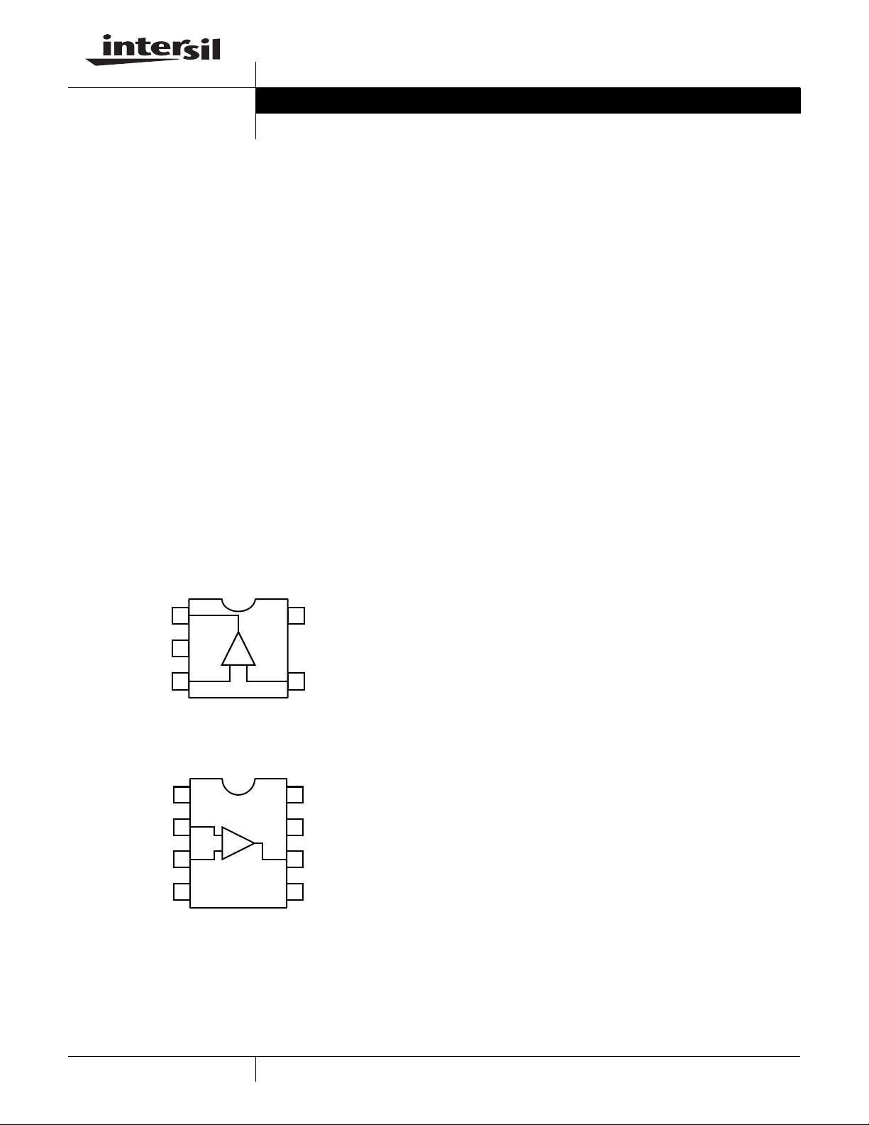
Pinouts
EL2126
(5 LD SOT-23)
TOP VIEW
Features
• Voltage noise of only 1.3nV/√Hz
• Current noise of only 1.2pA/√Hz
• 200µV offset voltage
• 100MHz -3dB BW for A
= 10
V
• Very low supply current - 4.7mA
• SOT-23 package
• ±2.5V to ±15V operation
• Pb-free plus anneal available (RoHS compliant)
Applications
• Ultrasound input amplifiers
• Wideband instrumentation
• Communication equipment
• AGC and PLL active filters
• Wideband sensors
OUT
VS-
NC
IN-
IN+
VS-
1
2
3
1
2
3
4
-+
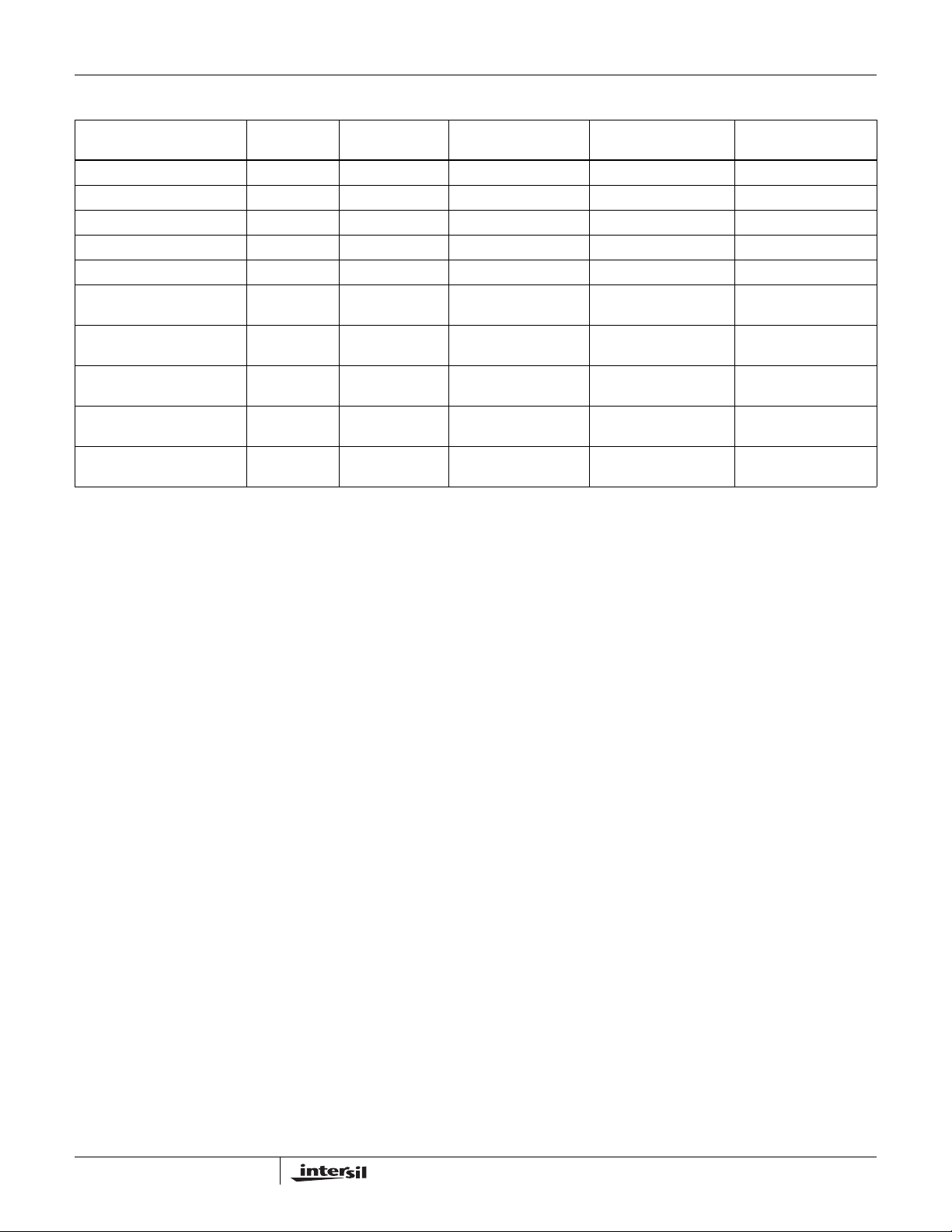
EL2126
(8 LD SOIC)
TOP VIEW
-
+
5
VS+
4
IN-IN+
NC
8
VS+
7
OUT
6
NC
5
1
CAUTION: These devices are sensitive to electrostatic discharge; follow proper IC Handling Procedures.
1-888-INTERSIL or 1-888-468-3774
| Intersil (and design) is a registered trademark of Intersil Americas Inc.
Copyright Intersil Americas Inc. 2002, 2005, 2007. All Rights Reserved
All other trademarks mentioned are the property of their respective owners.
Page 2
Ordering Information
EL2126
PART
NUMBER
EL2126CW-T7 G -40 to +85 7” (3k pcs) 5 Ld SOT-23 MDP0038
EL2126CW-T7A G -40 to +85 7” (250 pcs) 5 Ld SOT-23 MDP0038
EL2126CS 2126CS -40 to +85 - 8 Ld SOIC (150 mil) MDP0027
EL2126CS-T7 2126CS -40 to +85 7” 8 Ld SOIC (150 mil) MDP0027
EL2126CS-T13 2126CS -40 to +85 13” 8 Ld SOIC (150 mil) MDP0027
EL2126CSZ ( Note) 2126CSZ -40 to +85 - 8 Ld SOIC (150 mil)
EL2126CSZ-T7 ( Note) 2126CSZ -40 to +85 7” 8 Ld SOIC (150 mil)
EL2126CSZ-T13 ( Note) 2126CSZ -40 to +85 13” 8 Ld SOIC (150 mil)
EL2126CWZ-T7 (Note) BAAH -40 to +85 7” 5 Ld SOT-23 (SC74)
EL2126CWZ-T7A (Note) BAAH -40 to +85 7” 5 Ld SOT-23 (SC74)
NOTE: Intersil Pb-free products employ special Pb-free material sets; molding compounds/die attach materials and 100% matte tin plate termination
finish, which are RoHS compliant and compatible with both SnPb and Pb-free soldering operations. Intersil Pb-free products are MSL classified at
Pb-free peak reflow temperatures that meet or exceed the Pb-free requirements of IPC/JEDEC J STD-020.
PART
MARKING
TEMP RANGE
(°C) TAPE AND REEL PACKAGE PKG. DWG. #
MDP0027
(Pb-free)
MDP0027
(Pb-free)
MDP0027
(Pb-free)
P5.064
(1.65mm) (Green)
P5.064
(1.65mm) (Green)
2
FN7046.4
May 2, 2007
Page 3
EL2126
Absolute Maximum Ratings Thermal Information
VS+ to VS-) . . . . . . . . . . . . . . . . . . . . . . . . . . . . . . . . . . . . . . . . .33V
Continuous Output Current . . . . . . . . . . . . . . . . . . . . . . . . . . . 40mA
Any Input . . . . . . . . . . . . . . . . . . . . . . . . . . . V
CAUTION: Stresses above those listed in “Absolute Maximum Ratings” may cause permanent damage to the device. This is a stress only rating and operation of the
device at these or any other conditions above those indicated in the operational sections of this specification is not implied.
IMPORTANT NOTE: All parameters having Min/Max specifications are guaranteed. Typical values are for information purposes only. Unless otherwise noted, all tests
are at the specified temperature and are pulsed tests, therefore: TJ = TC = T
+ -0.3V to VS- +0.3V
S
A
Operating Temperature . . . . . . . . . . . . . . . . . . . . . . .-40°C to +85°C
Storage Temperature. . . . . . . . . . . . . . . . . . . . . . . .-60°C to +150°C
Maximum Die Junction Temperature. . . . . . . . . . . . . . . . . . .+150°C
Power Dissipation . . . . . . . . . . . . . . . . . . . . . . . . . . . . . . . . . See Curves
Pb-free reflow profile . . . . . . . . . . . . . . . . . . . . . . . . . .see link below
http://www.intersil.com/pbfree/Pb-FreeReflow.asp
Electrical Specifications V
+ = +5V, VS- = -5V, TA = +25°C, RF = 180Ω, RG = 20Ω, RL = 500Ω Unless Otherwise Specified.
S
Parameter Description Conditions Min Typ Max Unit
DC PERFORMANCE
V
OS
Input Offset Voltage (SO8) 0.2 2 mV
Input Offset Voltage (SOT23-5) 3mV
T
CVOS
I
B
I
OS
T
CIB
C
IN
A
VOL
PSRR Power Supply Rejection Ratio
Offset Voltage Temperature
17 µV/°C
Coefficient
Input Bias Current -10 -7 µA
Input Bias Current Offset 0.06 0.6 µA
Input Bias Current Temperature
0.013 µA/°C
Coefficient
Input Capacitance 2.2 pF
Open Loop Gain VO = -2.5V to +2.5V 80 87 dB
80 100 dB
(Note 1)
CMRR Common Mode Rejection Ratio at CMIR 75 106 dB
CMIR Common Mode Input Range -4.6 3.8 V
V
OUTH
V
OUTL
V
OUTH2
V
OUTL2
I
OUT
I
SY
AC PERFORMANCE - R
BW -3dB Bandwidth, R
BW ±0.1dB ±0.1dB Bandwidth, R
BW ±1dB ±1dB Bandwidth, R
Peaking Peaking, R
SR Slew Rate V
OS Overshoot, 4V
t
S
Positive Output Voltage Swing No load, RF = 1kΩ 3.8 3.8 V
Negative Output Voltage Swing No load, RF = 1kΩ -4 -3.9 V
Positive Output Voltage Swing RL = 100Ω 3.2 3.45 V
Negative Output Voltage Swing RL = 100Ω -3.5 -3.2 V
Output Short Circuit Current
80 100 mA
(Note 2)
Supply Current 4.7 5.5 mA
= 20Ω, CL = 3pF
G
= 500Ω 100 MHz
L
= 500Ω 17 MHz
L
= 500Ω 80 MHz
L
= 500Ω 0.6 dB
L
Wave
Output Square
P-P
= 2V
OUT
Positive 2.8 %
Negative -7 %
, measured at 20% to 80% 80 110 V/µs
P-P
Settling Time to 0.1% of ±1V Pulse 51 ns
3
FN7046.4
May 2, 2007
Page 4
EL2126
Electrical Specifications V
+ = +5V, VS- = -5V, TA = +25°C, RF = 180Ω, R
S
: , R
G
: Unless Otherwise Specified.
L
Parameter Description Conditions Min Typ Max Unit
V
N
I
N
Voltage Noise Spectral Density 1.3 nV/√Hz
Current Noise Spectral Density 1.2 pA/√Hz
HD2 2nd Harmonic Distortion (Note 3) -70 dBc
HD3 3rd Harmonic Distortion (Note 3) -70 dBc
NOTES:
1. Measured by moving the supplies from ±4V to ±6V
2. Pulse test only and using a 10Ω load
3. Frequency = 1MHz, V
OUT
= 2V
Electrical Specifications V
P-P
+ = +15V, VS- = -15V, TA = 25°C, R
S
: and 5pF load
: , R
F
= 20Ω, R
G
: unless otherwise specified.
L
Parameter Description Conditions Min Typ Max Unit
DC PERFORMANCE
V
OS
Input Offset Voltage (SO8) 0.5 3 mV
Input Offset Voltage (SOT23-5) 3mV
T
CVOS
Offset Voltage Temperature
4.5 µV/°C
Coefficient
I
I
T
B
OS
CIB
Input Bias Current -10 -7 µA
Input Bias Current Offset 0.12 0.7 µA
Input Bias Current Temperature
0.016 µA/°C
Coefficient
C
IN
A
VOL
PSRR Power Supply Rejection Ratio
Input Capacitance 2.2 pF
Open Loop Gain 80 90 dB
65 80 dB
(Note 4)
CMRR Common Mode Rejection Ratio at CMIR 70 85 dB
CMIR Common Mode Input Range -14.6 13.8 V
V
OUTH
V
OUTL
V
OUTH2
V
OUTL2
I
OUT
Positive Output Voltage Swing No load, R
Negative Output Voltage Swing No load, R
Positive Output Voltage Swing R
Negative Output Voltage Swing R
L
L
Output Short Circuit Current
: 13.6 13.7 V
F
: -13.8 -13.7 V
F
: , RF = 1k: 10.2 11.2 V
: , RF = 1k: -10.3 -9.5 V
140 220 mA
(Note 5)
I
SY
AC PERFORMANCE - R
BW -3dB Bandwidth, R
BW ±0.1dB ±0.1dB Bandwidth, R
BW ±1dB ±1dB Bandwidth, R
Peaking Peaking, R
SR Slew Rate (±2.5V Square Wave,
Supply Current 56mA
= 20: , CL = 3pF
G
: 135 MHz
L
: 26 MHz
L
: 60 MHz
L
: 2.1 dB
L
130 150 V/µS
Measured 25%-75%)
OS Overshoot, 4V
Wave
T
S
Settling Time to 0.1% of ±1V Pulse 48 ns
Output Square
P-P
Positive 1.6 %
Negative -4.4 %
4
FN7046.4
May 2, 2007
Page 5
Electrical Specifications V
+ = +15V, VS- = -15V, TA = 25°C, RF = 180Ω, RG = 20Ω, RL = 500Ω unless otherwise specified. (Continued)
S
Parameter Description Conditions Min Typ Max Unit
V
N
I
N
Voltage Noise Spectral Density 1.4 nV/√Hz
Current Noise Spectral Density 1.1 pA/√Hz
HD2 2nd Harmonic Distortion (Note 6) -72 dBc
HD3 3rd Harmonic Distortion (Note 6) -73 dBc
NOTES:
4. Measured by moving the supplies from ±13.5V to ±16.5V
5. Pulse test only and using a 10Ω load
6. Frequency = 1MHz, V
OUT
= 2V
, into 500Ω and 5pF load
P-P
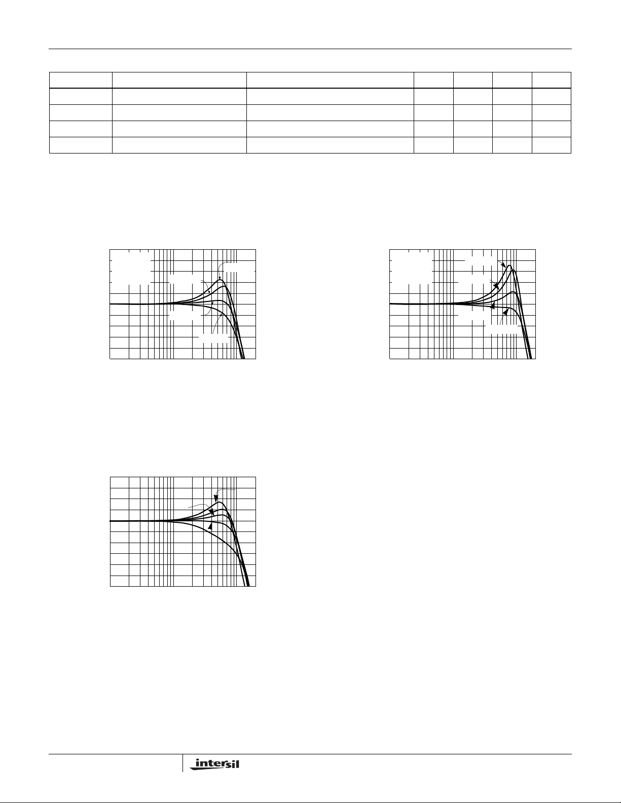
Typical Performance Curves
10
VS = ±5V
= 10
A
V
C
= 5pF
6
L
RL = 500Ω
2
-2
-6
NORMALIZED GAIN (dB)
-10
1M 10M 100M
RF = 500Ω
RF = 180Ω
FREQUENCY (Hz)
RF = 1kΩ
RF = 100Ω
FIGURE 1. NON-INVERTING FREQUENCY RESPONSE FOR
VARIOUS RF
8
4
0
-4
10
VS = ±15V
= 10
A
V
C
= 5pF
6
L
RL = 500Ω
2
-2
-6
NORMALIZED GAIN (dB)
-10
1M 10M 100M
RF = 1kΩ
RF = 500Ω
RF = 180Ω
RF = 100Ω
FREQUENCY (Hz)
FIGURE 2. NON-INVERTING FREQUENCY RESPONSE FOR
VARIOUS RF
-8
NORMALIZED GAIN (dB)
-12
1M 10M 100M
FREQUENCY (Hz)
FIGURE 3. INVERTING FREQUENCY RESPONSE FOR
VARIOUS RF
5
FIGURE 4. INVERTING FREQUENCY RESPONSE FOR
VARIOUS RF
May 2, 2007
FN7046.4
Page 6
Typical Performance Curves (Continued)
FIGURE 5. NON-INVERTING FREQUENCY RESPONSE FOR
VARIOUS GAIN
FIGURE 7. INVERTING FREQUENCY RESPONSE FOR
VARIOUS GAIN
FIGURE 6. NON-INVERTING FREQUENCY RESPONSE FOR
VARIOUS GAIN
FIGURE 8. INVERTING FREQUENCY RESPONSE FOR
VARIOUS RF
FIGURE 9. NON-INVERTING FREQUENCY RESPONSE FOR
VARIOUS OUTPUT SIGNAL LEVELS
6
FIGURE 10. NON-INVERTING FREQUENCY RESPONSE FOR
VARIOUS OUTPUT SIGNAL LEVELS
FN7046.4
May 2, 2007
Page 7

Typical Performance Curves (Continued)
EL2126
8
VS = ±5V
CL = 5pF
RL = 500Ω
4
RF = 350Ω
AV = 10
0
-4
-8
NORMALIZED GAIN (dB)
-12
1M 10M 100M
VO = 1V
VO = 3.4V
VO = 2.5V
FREQUENCY (Hz)
PP
PP
PP
VO = 500mV
VO = 30mV
PP
PP
FIGURE 11. INVERTING FREQUENCY RESPONSE FOR
VARIOUS OUTPUT SIGNAL LEVELS
10
VS = ±5V
RF = 150Ω
AV = 10
6
RL = 500Ω
2
-2
-6
NORMALIZED GAIN (dB)
CL = 28pF
CL = 16pFCL = 11pF
CL = 5pF
CL = 1pF
8
VS = ±15V
CL = 5pF
RL = 500Ω
4
RF = 200Ω
AV = 10
0
-4
-8
NORMALIZED GAIN (dB)
-12
1M 10M 100M
VO = 1V
VO = 3.4V
VO=2.5V
VO = 2.5V
FREQUENCY (Hz)
PP
P
PP
VO = 500mV
PP
VO = 30mV
PP
PP
FIGURE 12. INVERTING FREQUENCY RESPONSE FOR
VARIOUS OUTPUT SIGNAL LEVELS
10
VS = ±15V
6
2
-2
-6
NORMALIZED GAIN (dB)
RF = 180Ω
AV = 10
RL = 500Ω
CL = 28pF
CL = 16pF
CL = 5pF
CL = 11pF
CL = 1.2pF
-10
1M 10M 100M
FREQUENCY (Hz)
FIGURE 13. NON-INVERTING FREQUENCY RESPONSE FOR
VARIOUS CL
8
VS = ±5V
R
= 350Ω
F
RL = 500Ω
4
= -10
A
V
0
-4
-8
NORMALIZED GAIN (dB)
-12
1M 10M 100M
CL = 16pF
CL = 11pF
CL = 5pF
FREQUENCY (Hz)
CL = 28pF
CL = 1.2pF
FIGURE 15. INVERTING FREQUENCY RESPONSE FOR
VARIOUS CL
-10
1M 10M 100M
FREQUENCY (Hz)
FIGURE 14. NON-INVERTING FREQUENCY RESPONSE FOR
VARIOUS CL
8
VS = ±15V
= 200Ω
R
F
RL = 500Ω
4
A
= -10
V
0
-4
-8
NORMALIZED GAIN (dB)
-12
1M 10M 100M
CL = 16pF
CL=11p
CL = 11pF
FREQUENCY (Hz)
CL = 28pF
CL = 5pF
CL = 1.2pF
FIGURE 16. INVERTING FREQUENCY RESPONSE FOR
VARIOUS CL
7
FN7046.4
May 2, 2007
Page 8

Typical Performance Curves (Continued)
EL2126
100
GAIN
80
60
40
OPEN LOOP GAIN (dB)
20
VS=±5V
0
10k 10M 1G
100k 100M1M
FREQUENCY (Hz)
PHASE
250
150
50
-50
-150
-250
0.6/DIV
OPEN LOOP PHASE (°)
SUPPLY CURRENT (mA)
0
0
1.5/DIV
SUPPLY VOLTAGE (V)
FIGURE 17. OPEN LOOP GAIN AND OPEN LOOP PHASE FIGURE 18. SUPPLY CURRENT vs SUPPLY VOLTAGE
160
VS = ±5V
140
RG = 20Ω
RL = 500Ω
120
CL = 5pF
100
80
60
-3dB BANDWIDTH
40
20
0
0246810 1416
AV = -10
AV = -20
AV = -50
12
±VS (V)
FIGURE 19. BANDWIDTH vs Vs
AV = 10
AV = -20
AV = 50
3.0
VS = ±5V
RG = 20Ω
2.5
RL = 500Ω
CL = 5pF
2.0
1.5
1.0
PEAKING (dB)
0.5
0
0246810 1416
AV = 10
AV = -10
12
±SUPPLY VOLTAGE (V)
FIGURE 20. PEAKING vs Vs
= 20Ω
VS = ±5V
V
= 2V
O
PP
10ns/DIV
0.5V/DIV
RF = 180Ω
R
G
FIGURE 21. LARGE SIGNAL STEP RESPONSE
8
20mV/DIV
RF = 180Ω
RG = 20Ω
VS = ±5V
VO = 100mV
PP
10ns/DIV
FIGURE 22. SMALL SIGNAL STEP RESPONSE
FN7046.4
May 2, 2007
Page 9

Typical Performance Curves (Continued)
EL2126
-40
VS = ±5V
VO = 2V
-50
-60
-70
-80
-90
HARUMONIC DISTORTION (dBc)
-100
P-P
RF = 180Ω
AV = 10
RL = 500Ω
012345 78
3rd HD
V
OUT
2nd HD
(V
P-P
6
)
FIGURE 23. 1MHz HARMONIC DISTORTION vs OUTPUT
SWING
-20
VS = ±5V
VO = 2V
-30
-40
-50
-60
THD (dBc)
-70
-80
-90
1k 10k 100M
P-P
100k 1M 10M
FREQUENCY (Hz)
FIGURE 25. TOTAL HARMONIC DISTORTION vs FREQUENCY
-30
VS = ±5V
VO = 2V
HARMONIC DISTORTION (dBc)
-40
-50
-60
-70
-80
-90
-100
P-P
RF = 180Ω
AV = 10
RL = 500Ω
0 5 10 15 20 25
V
OUT
2nd HD
3rd HD
(V
)
P-P
FIGURE 24. 1MHz HARMONIC DISTORTION vs OUTPUT
SWING
10
(nV/√Hz)
N
(pA/√Hz), V
N
I
IN, VS = ±15V
1
10 100 10k 100k
IN, VS = ±5V
VN, VS = ±15V
VN, VS = ±5V
1k
FREQUENCY (Hz)
FIGURE 26. NOISE vs FREQUENCY
70
60
50
40
30
20
SETTLING TIME (ns)
10
0
0.1 1.0 10.0
V
V
S
=
V
S
=
±5V
V
S
=
±
1
5
V
ACCURACY (%)
S
=
±
5
V
,
V
O
=
5
V
P
-
±
1
5
V
,
V
, V
O
=
2
,
V
O
=
2
P
O
=
5
V
P
-
P
V
P
-
P
V
P
-
P
FIGURE 27. SETTLING TIME vs ACCURACY
9
16
VS = ±5V
R
= 500Ω
L
12
8
4
GROUP DELAY (ns)
0
-4
1M 10M 100M 400M
FREQUENCY (Hz)
AV = 10
AV = -10
FIGURE 28. GROUP DELAY vs FREQUENCY
FN7046.4
May 2, 2007
Page 10

Typical Performance Curves (Continued)
EL2126
-10
-30
-50
-70
CMRR (dB)
-90
-110
10 1M 10M 100M
1k 100k100 10k
FREQUENCY (Hz)
FIGURE 29. CMRR vs FREQUENCY FIGURE 30. PSRR vs FREQUENCY
100
VS = ±5V
10
1
0.1
0.01
CLOSED LOOP OUTPUT IMPEDANCE (Ω)
10k 1M 100M
100k 10M
FREQUENCY (Hz)
FIGURE 31. CLOSED LOOP OUTPUT IMPEDANCE vs
FREQUENCY
110
90
70
50
PSRR (dB)
30
10
10k 100k 1M 10M 200M
120
100
80
60
BANDWIDTH (MHz)
40
20
PEAKING
0
-40 40 160
PSRR-
PSRR+
FREQUENCY (Hz)
BANDWIDTH
800120
TEMPERATURE (°C)
VS=±5V
VS = ±5V
3.5
3
2.5
2
1.5
1
0.5
0
-0.5
PEAKING (dB)
FIGURE 32. BANDWIDTH AND PEAKING vs TEMPERATURE
SLEW RATE (V/µs)
220
200
180
160
140
120
100
80
60
-1
15913
15VSR-
15VSR+
5VSR-
5VSR+
371115
V
SWING (VPP)
OUT
FIGURE 33. SLEW RATE vs SWING
10
5.2
5.1
5
(mA)
S
I
4.9
4.8
-50 0 100 15050
DIE TEMPERATURE (°C)
VS=±15V
VS=±5V
FIGURE 34. SUPPLY CURRENT vs TEMPERATURE
May 2, 2007
FN7046.4
Page 11

11
Page 12

Typical Performance Curves (Continued)
EL2126
-13.76
-13.78
(V)
OUTL
V
-13.8
-13.82
VS = ±15V
-50 0 100 15050
DIE TEMPERATURE (°C)
FIGURE 41. NEGATIVE OUTPUT SWING vs TEMPERATURE
155
150
VS = ±15V
145
SR (V/µs)
140
102
100
98
96
94
92
SLEW RATE (V/µs)
90
88
-50 0 100 15050
VS = ±5V
DIE TEMPERATURE (°C)
FIGURE 42. SLEW RATE vs TEMPERATURE
3.52
3.5
(V)
3.48
OUTH2
V
3.46
VS = ±5V
VO = 2V
135
-50 0 100 15050
PP
DIE TEMPERATURE (°C)
3.44
-50 0 100 15050
DIE TEMPERATURE (°C)
FIGURE 43. SLEW RATE vs TEMPERATURE FIGURE 44. POSITIVE LOADED OUTPUT SWING vs
TEMPERATURE
11.8
11.6
11.4
11.2
SR (V/µs)
11
10.8
10.6
-50 0 100 15050
VS = ±15V
DIE TEMPERATURE (°C)
FIGURE 45. POSITIVE LOADED OUTPUT SWING vs
TEMPERATURE
FIGURE 46. NEGATIVE LOADED OUTPUT SWING vs
-3.35
-3.4
-3.45
(V)
OUTL2
-3.5
V
3.55
-3.6
-50 0 100 15050
TEMPERATURE
VS = ±5V
DIE TEMPERATURE (°C)
12
FN7046.4
May 2, 2007
Page 13

Typical Performance Curves (Continued)
-9.4
-9.6
-9.8
(V)
-10
OUTL2
V
-10.2
-10.4
-10.6
-50 0 100 15050
FIGURE 47. NEGATIVE LOADED OUTPUT SWING vs TEMPERATURE
JEDEC JESD51-3 LOW EFFECTIVE THERMAL
CONDUCTIVITY TEST BOARD
1.2
0.6
POWER DISSIPATION (W)--23374.88.7 2.17 0 8.0062 Tc(50)Tj-4758 -1.TD3.196.000901.6
0
0
AMBIENT Temperature (°C)
FIGURE 48. PACKAGE POWER DISSIP A TION vs AMBIENT
TEMPERATURE
VS=±15V
Die Temperature (°C)
FIGURE 49. PACKAGE POWER DISSIP A TION vs AMBIENT
TEMPERATURE
13
FN7046.4
May 2, 2007
Page 14

Pin Descriptions
EL2126
EL2126CW
(5 Ld SOT-23)
EL2126CS
( 8 Ld SOIC) PIN NAME PIN FUNCTION EQUIVALENT CIRCUIT
1 6 VOUT Output
2 4 VS- Supply
3 3 VINA+ Input
4 2 VINA- Input Reference Circuit 2
5 7 VS+ Supply
VS+
Circuit 1
VS-
Circuit 2
VS+
V
OUT
VIN-VIN+
14
FN7046.4
May 2, 2007
Page 15

EL2126
Applications Information
Product Description
The EL2126 is an ultra-low noise, wideband monolithic
operational amplifier built on Elantec's proprietary high
speed complementary bipolar process. It features 1.3nV/√Hz
input voltage noise, 200µV typical offset voltage, and 73dB
THD. It is intended for use in systems such as ultrasound
imaging where very small signals are needed to be
amplified. The EL2126 also has excellent DC specifications:
200µV V
specifications allow the EL2126 to be used in DC-sensitive
applications such as difference amplifiers.
Gain-Bandwidth Product
The EL2126 has a gain-bandwidth product of 650MHz at
±5V. For gains less than 20, higher-order poles in the
amplifier's transfer function contribute to even higher closedloop bandwidths. For example, the EL2126 has a -3dB
bandwidth of 100MHz at a gain of 10 and decreases to
33MHz at gain of 20. It is important to note that the extra
bandwidth at lower gain does not come at the expenses of
stability. Even though the EL2126 is designed for gain ≥ 10.
With external compensation, the device can also operate at
lower gain settings. The RC network show n in Figure 50
reduces the feedback gain at high frequency and thus
maintains the amplifier stability. R values must be less than
RF divided by 9 and 1 divided by 2
200MHz.
Choice of Feedback Resistor, RF
The feedback resistor forms a pole with the input
capacitance. As this pole becomes larger, phase margin is
reduced. This increases ringing in the time domain and
peaking in the frequency domain. Therefore, RF has some
maximum value which should not be exceeded for optimum
performance. If a large value of RF must be used, a small
capacitor in the few pF range in parallel with RF can help to
reduce this ringing and peaking at the expense of reducing
the bandwidth. Frequency response curves for various RF
values are shown in the typical performance curves section
of this data sheet.
, 22µA IB, 0.4µA IOS, and 106dB CMRR. These
OS
πRC must be less than
R
F
R
C
V
IN
-
+
FIGURE 50.
V
OUT
Noise Calculations
The primary application for the EL2126 is to amplify very
small signals. To maintain the proper signal-to-noise ratio, it
is essential to minimize noise contribution from the amplifier.
Figure 51 shows all the noise sources for all the components
around the amplifier.
R
V
V
IN+ is the amplifier positive input current noise
I
N
VRX is the thermal noise associated with each resistor:
V
RX
where:
k is Boltzmann's constant = 1.380658 x 10
T is temperature in degrees Kelvin (273 + °C)
The total noise due to the amplifier seen at the output of the
amplifier can be calculated by using the Equation 2.
As the equation shows, to keep noise at a minimum, small
resistor values should be used. At higher amplifier gain
configuration where R
and R
starts to dominate. Because noise is summed in a rootmean-squares method, noise sources smaller than 25% of
the largest noise source can be ignored. This can greatly
simplify the formula and make noise calculation much easier
to calculate.
3
IN
V
R3
IN+
IN-
V
N
+
-
V
R1
R
1
V
R2
R
2
V
ON
FIGURE 51.
is the amplifier input voltage noise
N
- is the amplifier negative input current noise
4kTRx=
-23
is reduced, the noise due to IN-, R2,
decreases and the noise caused by IN+, VN, and R3
1
2
(EQ. 1)
2
V
ON
⎛ ⎞
BW= VN21
×
⎜ ⎟
⎝ ⎠
R
⎛⎞
1
-------
× IN-2R
+
⎜⎟
R
⎝⎠
2
2
1
IN+2R
⎛⎞
2
××+× 4KTR14KTR
⎜⎟
3
⎝⎠
2
R
1
-------
1
+
R
2
2
2
R
⎛⎞
1
-------
××××+××× 4KTR31
⎜⎟
R
⎝⎠
2
⎛⎞
××××++ +
⎜⎟
⎝⎠
2
R
1
-------
+
R
2
(EQ. 2)
15
FN7046.4
May 2, 2007
Page 16

EL2126
Output Drive Capability
The EL2126 is designed to drive low impedance load. It can
easily drive 6V
drive capability makes the EL2126 an ideal choice for RF , IF,
and video applications. Furthermore, the EL2126 is
current-limited at the output, allowing it to withstand
momentary short to ground. However, the power dissipation
with output-shorted cannot exceed the power dissipation
capability of the package.
signal into a 100Ω load. This high output
P-P
Driving Cables and Capacitive Loads
Although the EL2126 is designed to drive low impedance
load, capacitive loads will decreases the amplifier's phase
margin. As shown in the performance curves, capacitive
load can result in peaking, overshoot and possible
oscillation. For optimum AC performance, capacitive loads
should be reduced as much as possible or isolated with a
series resistor between 5Ω to 20Ω. When driving coaxial
cables, double termination is always recommended for
reflection-free performance. When properly terminated, the
capacitance of the coaxial cable will not add to the capacitive
load seen by the amplifier.
Power Supply Bypassing And Printed Circuit
Board Layout
As with any high frequency devices, good printed circuit
board layout is essential for optimum performance. Ground
plane construction is highly recommended. Lead lengths
should be kept as short as possible. The power supply pins
must be closely bypassed to reduce the risk of oscillation.
The combination of a 4.7µF tantalum capacitor in parallel
with 0.1µF ceramic capacitor has been proven to work well
when placed at each supply pin. For single supply operation,
where pin 4 (V
4.7µF tantalum capacitor in parallel with a 0.1µF ceramic
capacitor across pins 7 (V
For good AC performance, parasitic capacitance should be
kept to a minimum. Ground plane construction again should
be used. Small chip resistors are recommended to minimize
series inductance. Use of sockets should be avoided since
they add parasitic inductance and capacitance which will
result in additional peaking and overshoot.
-) is connected to the ground plane, a single
S
+) and pin 4 (VS-) will suffice.
S
Supply Voltage Range and Single Supply
Operation
The EL2126 has been designed to operate with supply
voltage range of ±2.5V to ±15V. With a single supply, the
EL2126 will operate from +5V to +30V. Pins 4 and 7 are the
power supply pins. The positive power supply is connected
to pin 7. When used in single supply mode, pin 4 is
connected to ground. When used in dual supply mode, the
negative power supply is connected to pin 4.
As the power supply voltage de creases from +30V to +5V, it
becomes necessary to pay special attention to the input
voltage range. The EL2126 has an input voltage range of
0.4V from the negative supply to 1.2V from the positive
supply. So, for example, on a single +5V supply, the EL2126
has an input voltage range which spans from 0.4V to 3.8V.
The output range of the EL2126 is also quite large, on a +5V
supply, it swings from 0.4V to 3.8V.
16
FN7046.4
May 2, 2007
Page 17

Small Outline Package Family (SO)
A
D
NN
(N/2)+1
EL2126
h X 45°
PIN #1
E
C
SEATING
PLANE
0.004 C
E1
B
0.010 BM CA
I.D. MARK
1
e
0.010 BM CA
(N/2)
c
SEE DETAIL “X”
L1
H
A2
GAUGE
PLANE
A1
b
DETAIL X
L
4° ±4°
MDP0027
SMALL OUTLINE PACKAGE FAMILY (SO)
INCHES
SO16
SYMBOL
(0.150”)
A 0.068 0.068 0.068 0.104 0.104 0.104 0.104 MAX -
A1 0.006 0.006 0.006 0.007 0.007 0.007 0.007 ±0.003 -
A2 0.057 0.057 0.057 0.092 0.092 0.092 0.092 ±0.002 -
b 0.017 0.017 0.017 0.017 0.017 0.017 0.017 ±0.003 -
c 0.009 0.009 0.009 0.011 0.011 0.011 0.011 ±0.001 -
D 0.193 0.341 0.390 0.406 0.504 0.606 0.704 ±0.004 1, 3
E 0.236 0.236 0.236 0.406 0.406 0.406 0.406 ±0.008 E1 0.154 0.154 0.154 0.295 0.295 0.295 0.295 ±0.004 2, 3
e 0.050 0.050 0.050 0.050 0.050 0.050 0.050 Basic -
L 0.025 0.025 0.025 0.030 0.030 0.030 0.030 ±0.009 L1 0.041 0.041 0.041 0.056 0.056 0.056 0.056 Basic -
h 0.013 0.013 0.013 0.020 0.020 0.020 0.020 Reference -
N 8 14 16 16 20 24 28 Reference -
NOTES:
1. Plastic or metal protrusions of 0.006” maximum per side are not included.
2. Plastic interlead protrusions of 0.010” maximum per side are not included.
3. Dimensions “D” and “E1” are measured at Datum Plane “H”.
4. Dimensioning and tolerancing per ASME Y14.5M-1994
SO16 (0.300”)
(SOL-16)
SO20
(SOL-20)
SO24
(SOL-24)
SO28
(SOL-28)
TOLERANCE NOTESSO-8 SO-14
A
0.010
Rev. M 2/07
17
FN7046.4
May 2, 2007
Page 18

EL2126
Small Outline Transistor Plastic Packages (SOT23-5)
D
e1
E
C
L
E1
C
18
FN7046.4
May 2, 2007
Page 19

SOT-23 Package Family
EL2126
2 3
0.15 DC
2X
C
SEATING
PLANE
E1
5
0.15 A-BC
2X
0.10 C
NX
(L1)
e1
A
6
N
4
D
MDP0038
SOT-23 PACKAGE FAMILY
SYMBOL
MILLIMETERS
TOLERANCESOT23-5 SOT23-6
A 1.45 1.45 MAX
A1 0.10 0.10 ±0.05
E
A2 1.14 1.14 ±0.15
b 0.40 0.40 ±0.05
321
e
0.20
B
b
NX
M
0.20 C
2X
DC A-B
c 0.14 0.14 ±0.06
D 2.90 2.90 Basic
E 2.80 2.80 Basic
E1 1.60 1.60 Basic
e 0.95 0.95 Basic
e1 1.90 1.90 Basic
L 0.45 0.45 ±0.10
L1 0.60 0.60 Reference
1 3
D
N 5 6 Reference
Rev. F 2/07
NOTES:
A2
1. Plastic or metal protrusions of 0.25mm maximum per side are not
included.
2. Plastic interlead protrusions of 0.25mm maximum per side are not
A1
included.
3. This dimension is measured at Datum Plane “H”.
4. Dimensioning and tolerancing per ASME Y14.5M-1994.
5. Index area - Pin #1 I.D. will be located within the indicated zone
(SOT23-6 only).
H
6. SOT23-5 version has no center lead (shown as a dashed line).
A
c
L
0°
GAUGE
PLANE
+3°
-0°
0.25
All Intersil U.S. products are manufactured, assembled and tested utilizing ISO9000 quality systems.
Intersil Corporation’s quality certifications can be viewed at www.intersil.com/design/quality
Intersil products are sold by description only. Intersil Corporation reserves the right to make changes in circuit design, software and/or specifications at any time without
notice. Accordingly, the reader is cautioned to verify that data sheets are current before placing orders. Information furnished by Intersil is believed to be accurate and
reliable. However, no responsibility is assumed by Intersil or its subsidiaries for its use; nor for any infringements of patents or other rights of third parties which may result
from its use. No license is granted by implicat ion or oth erwise u nde r any p a tent or p at ent r ights of Intersil or its subsidiari es.
For information regarding Intersil Corporation and its products, see www.intersil.com
19
FN7046.4
May 2, 2007
 Loading...