

Page 1
www.BDTIC.com/Intersil
®
EL1511
Data Sheet April 10, 2007
Medium Power Differential Line Driver
The EL1511 is a dual operational amplifier designed for
customer premise line driving in DMT ADSL solutions. This
device features a high drive capability of 360mA while
consuming only 7.5mA of supply current per amplifier and
operating from a single 5V to 15V supply. This driver
achieves a typical distortion of less than -85dBc, at 150kHz
into a 25Ω load. The EL1511 is available in the th ermallyenhanced 16 Ld SOIC (0.150") and a 16 Ld QFN (4x4mm)
packages. The EL1511 is specified for operation over the full
-40°C to +85°C temperature range. Electrical characteristics
are given for typical 15V supply operation.
The EL1511 has two control pins, C
the selection of full I
power , 3/ 4-IS, 1/2-IS, and power-down
S
modes.
The EL1511 is ideal for ADSL, SDSL, and HDSL2 line
driving applications for single power supply, high voltage
swing, and low power.
The EL1511 maintains excellent distortion and load driving
capabilities even in the lowest power settings.
and C1, which allow
0
FN7016.2
Features
• Drives up to 360mA from a +15V supply
•24V
differential output drive into 25Ω and 26V
P-P
P-P
differential output drive into 100Ω
• -85dBc typical driver output distortion at full output at
150kHz
• Low quiescent current of 3.5mA per amplifier at 1/2-I
current mode
• Disable down to 1.5mA
• Pb-free plus anneal available (RoHS compliant)
Applications
• ADSL CSA line driving
• ADSL full rate CPE line driving
• G.SHDSL, HDSL2 line driver
• Video distribution amplifier
• Video twisted-pair line driver
S
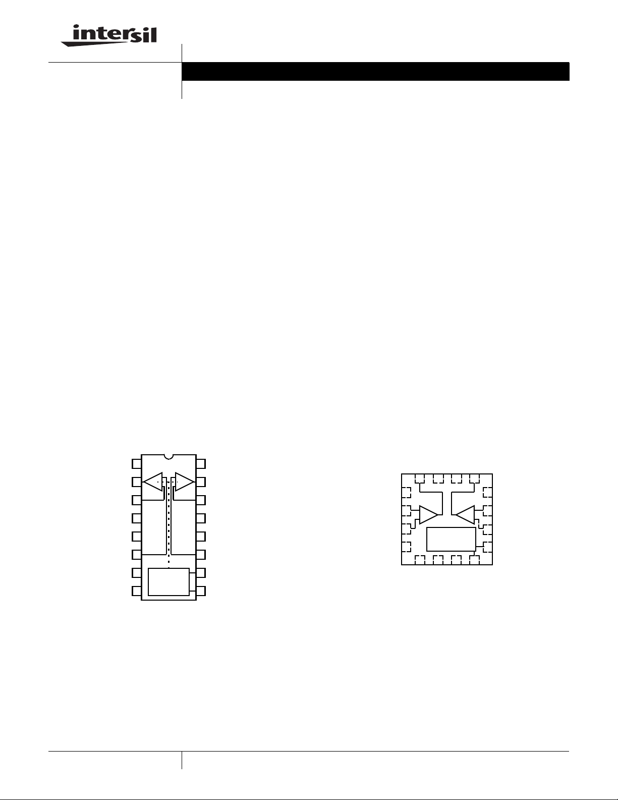
Pinouts
EL1511
[16 LD SO (0.150”)]
TOP VIEW
NC
1
VOUTA
VIN-A
GND*
GND*
VIN+A
GND
VS-
NOTE: * These GND pins are heat spreaders
+
2
-
3
4
5
6
POWER
7
CONTROL
LOGIC
8 9
16
+
15
14
13
12
11
10
VS+
VOUTB
VIN-B
GND*
GND*
VIN+B
C1
C0
NC
INA-
INA+
GND
(16 LD QFN)
TOP VIEW
OUTA
16
1
AMP AAMP
-
2
+
3
4
5
NC
EL1511
NC
VS+
15
14
B
POWER
CONTROL
LOGIC
7
6
NC
VS-
OUTB
13
NC
12
INB-
-
11
+
INB+
10
C1
9
8
C0
1
CAUTION: These devices are sensitive to electrostatic discharge; follow proper IC Handling Procedures.
1-888-INTERSIL or 1-888-468-3774
| Intersil (and design) is a registered trademark of Intersil Americas Inc.
Copyright Intersil Americas Inc. 2003, 2005, 2007. All Rights Reserved
All other trademarks mentioned are the property of their respective owners.
Page 2
www.BDTIC.com/Intersil
EL1511
Ordering Information
PART NUMBER PART MARKING TAPE & REEL PACKAGE PKG. DWG. #
EL1511CS EL1511CS - 16 Ld SO (0.150”) MDP0027
EL1511CS-T7 EL1511CS 7” 16 Ld SO (0.150”) MDP0027
EL1511CS-T13 EL1511CS 13” 16 Ld SO (0.150”) MDP0027
EL1511CSZ
(See Note)
EL1511CSZ-T7
(See Note)
EL1511CSZ-T13
(See Note)
EL1511CL 1511CL - 16 Ld QFN MDP0046
EL1511CL-T7 1511CL 7” 16 Ld QFN MDP0046
EL1511CL-T13 1511CL 13” 16 Ld QFN MDP0046
EL1511CLZ
(See Note)
EL1511CLZ-T7
(See Note)
EL1511CLZ-T13
(See Note)
NOTE: Intersil Pb-free plus anneal products employ special Pb-free material sets; molding compounds/die attach materials and 100% matte tin plate
termination finish, which are RoHS compliant and compatible with both SnPb and Pb-free soldering operations. Intersil Pb-free products are MSL
classified at Pb-free peak reflow temperatures that meet or exceed the Pb-free requirements of IPC/JEDEC J STD-020.
EL1511CSZ - 16 Ld SO (0.150”)
(Pb-Free)
EL1511CSZ 7” 16 Ld SO (0.150”)
(Pb-Free)
EL1511CSZ 13” 16 Ld SO (0.150”)
(Pb-Free)
1511CLZ - 16 Ld QFN
(Pb-Free)
1511CLZ 7” 16 Ld QFN
(Pb-Free)
1511CLZ 13” 16 Ld QFN
(Pb-Free)
MDP0027
MDP0027
MDP0027
MDP0046
MDP0046
MDP0046
2
FN7016.2
April 10, 2007
Page 3
www.BDTIC.com/Intersil
EL1511
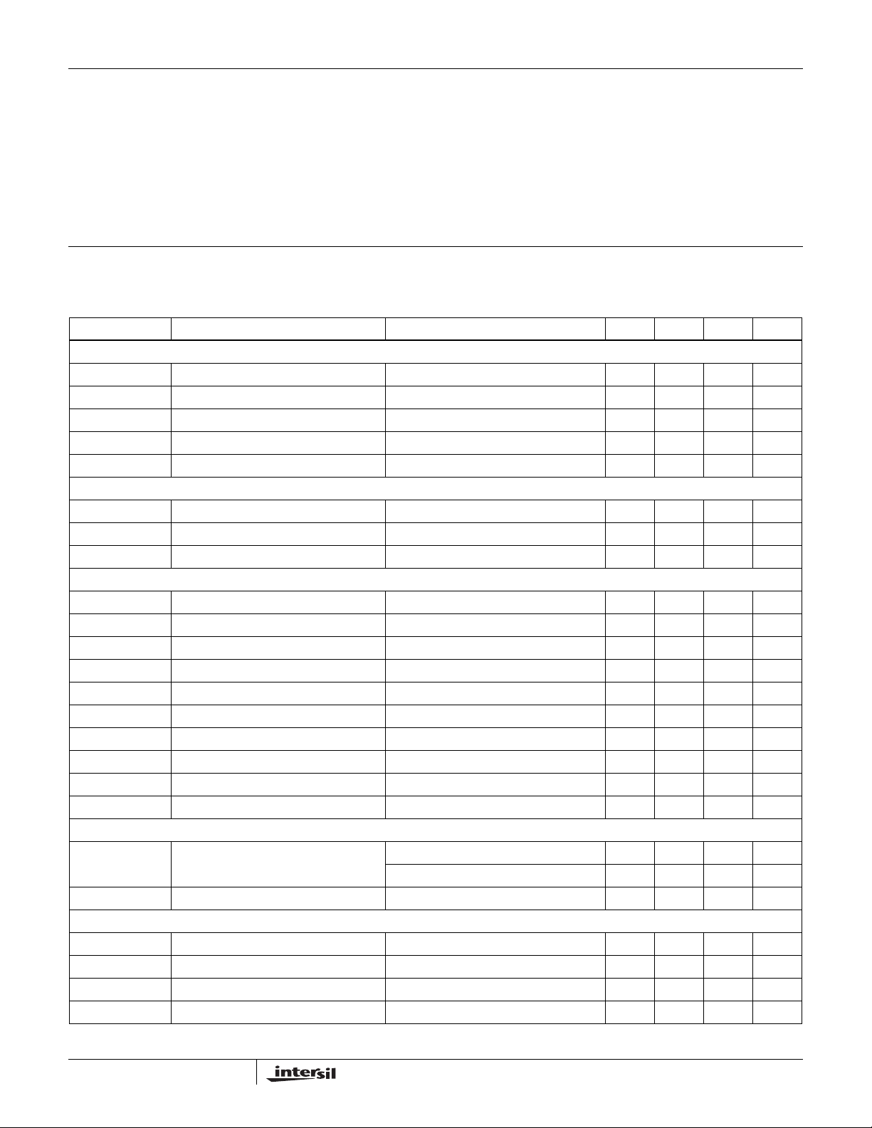
Absolute Maximum Ratings (T
V
+ to VS- Supply Voltage. . . . . . . . . . . . . . . . . . . . . . . . . . . . 16.5V
S
V
+ Voltage to Ground . . . . . . . . . . . . . . . . . . . . . . -0.3V to +16.5V
S
- Voltage to Ground. . . . . . . . . . . . . . . . . . . . . . . . -16.5V to 0.3V
V
S
Input C
V
IN
CAUTION: Stresses above those listed in “Absolute Maximum Ratings” may cause permanent damage to the device. This is a stress only rating and operation of the
device at these or any other conditions above those indicated in the operational sections of this specification is not implied.
IMPORTANT NOTE: All parameters having Min/Max specifications are guaranteed. Typical values are for information purposes only. Unless otherwise noted, all tests
are at the specified temperature and are pulsed tests, therefore: TJ = TC = T
to Ground. . . . . . . . . . . . . . . . . . . . . . . . . . . . . . . . . .7V
0/C1
+ Voltage . . . . . . . . . . . . . . . . . . . . . . . . . . . . . . . . . . VS- to VS+
Electrical Specifications V
= +25°C)
A
Current into any Input . . . . . . . . . . . . . . . . . . . . . . . . . . . . . . . . 8mA
Continuous Output Current . . . . . . . . . . . . . . . . . . . . . . . . . . . 75mA
Operating Temperature Range . . . . . . . . . . . . . . . . .-40°C to +85°C
Storage Temperature Range . . . . . . . . . . . . . . . . . .-60°C to +150°C
Operating Junction Temperature . . . . . . . . . . . . . . .-40°C to +150°C
Power Dissipation . . . . . . . . . . . . . . . . . . . . . . . . . . . . . See Curves
A
= ±7.5V, RF = 1.5kΩ, RL = 100Ω to mid supply, TA = +25°C unless otherwise specified.
S
PARAMETER DESCRIPTION CONDITIONS MIN TYP MAX UNIT
AC PERFORMANCE
BW -3dB Bandwidth A
HD Total Harmonic Distortion f = 150kHz, V
= +4 70 MHz
V
O
= 16V
, RL = 25Ω -85 dBc
P-P
dG Differential Gain AV = +2, RL = 37.5Ω 0.15 %
dθ Differential Phase A
SR Slewrate V
= +2, RL = 37.5Ω 0.1 °
V
from -3V to +3V 500 V/µs
OUT
DC PERFORMANCE
V
ΔV
R
OS
OS
OL
Offset Voltage -20 20 mV
VOS Mismatch -10 10 mV
Transimpedance V
from -4.5V to +4.5V 0.7 1.4 2.5 MΩ
OUT
INPUT CHARACTERISTICS
+ Non-Inverting Input Bias Current -5 5 µA
I
B
- Inverting Input Bias Current -30 30 µA
I
B
ΔIB-I
e
N
i
N
V
IH
V
IL
I
IH1
I
IH0
I
IL
- Mismatch -30 30 µA
B
Input Noise Voltage 2.8 nV/√Hz
-Input Noise Current 19 pA/√Hz
Input High Voltage C0 and C1 inputs 2.3 V
Input Low Voltage C0 and C1 inputs 1.5 V
Input High Current for C
Input High Current for C
1
0
Input Low Current for C1or C
0
C1 = 5V 0.2 8 µA
C0 = 5V 0.1 4 µA
C1 = 0V, C0 = 0V -1 1 µA
OUTPUT CHARACTERISTICS
V
I
OUT
OUT
Loaded Output Swing (single ended) VS = ±7.5, RL = 100Ω to GND ±6.3 ±6.5 V
= ±7.5, RL = 25Ω to GND ±5.7 ±6.0 V
V
S
Output Current RL = 0Ω 450 mA
SUPPLY
V
S
+ (Full Power) Positive Supply Current per Amplifier All outputs at 0V, C0 = C1 = 0V 7 9.25 mA
I
S
- (Full Power) Negative Supply Current per Amplifier All outputs at 0V, C0 = C1 = 0V -6.4 -8.75 mA
I
S
+ (3/4 Power) Positive Supply Current per Amplifier All outputs at 0V, C0 = 5V, C1 = 0V 5.3 7.25 mA
I
S
Supply Voltage Single supply 5 15 V
3
FN7016.2
April 10, 2007
Page 4
www.BDTIC.com/Intersil
V
EL1511
Electrical Specifications V
= ±7.5V, RF = 1.5kΩ, RL = 100Ω to mid supply, TA = +25°C unless otherwise specified. (Continued)
S
PARAMETER DESCRIPTION CONDITIONS MIN TYP MAX UNIT
IS- (3/4 Power) Negative Supply Current per Amplifier All outputs at 0V, C0 = 5V, C1 = 0V -4.7 -6.75 mA
+ (1/2 Power) Positive Supply Current per Amplifier All outputs at 0V, C0 = 0V, C1 = 5V 3.3 5.75 mA
I
S
- (1/2 Power) Negative Supply Current per Amplifier All outputs at 0V, C0 = 0V, C1 = 5V -2.7 -5.2 mA
I
S
+ (Power Down) Positive Supply Current per Amplifier All outputs at 0V, C0 = C1 = 5V 0.6 1.025 mA
I
S
- (Power Down) Negative Supply Current per Amplifier All outputs at 0V, C0 = C1 = 5V 0 -0.525 mA
I
S
I
GND
GND Supply Current per Amplifier All outputs at 0V 0.6 1 mA
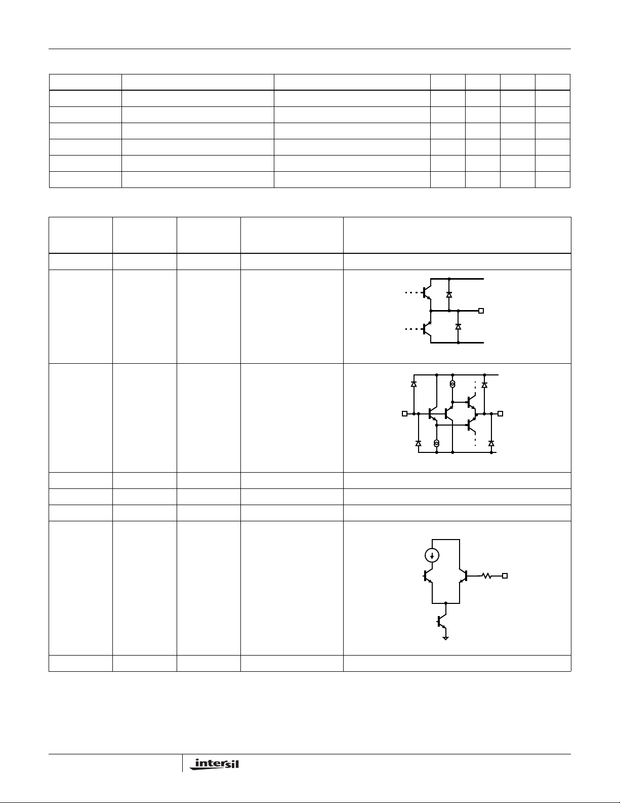
Pin Descriptions
EL1511CS
16 Ld SO
(0.150”)
1 1, 5, 6, 12, 15 NC Not Connected
2, 15 13, 16 OUT Output
3, 14 2, 11 VIN- Inverting Input
EL1511CL
16 Ld QFN PIN NAME PIN FUNCTION EQUIVALENT CIRCUIT
S
OUT
V
S
CIRCUIT 1
+
-
+
V
S
4, 5, 7, 12, 13 4 GND Ground Pins
6, 11 3, 10 VIN+ Non-inverting Input Reference Circuit 2
8 7 VS- Negative Supply
9 8 C0 Power Control
10 9 C1 Power Control Reference Circuit 3
I
BIAS
1.8V Q3Q1
CIRCUIT 2
VS+
+
–
Q2
CIRCUIT 3
500Ω C
IN-IN+
-
V
S
0
4
FN7016.2
April 10, 2007
Page 5
www.BDTIC.com/Intersil
Typical Performance Curves
EL1511
28
VS=±6V
A
=10
V
24
=100Ω
R
L
RF=1.5kΩ
20
16
GAIN (dB)
12
8
100K
1M 100M10M
RF=2kΩ
FREQUENCY (Hz)
RF=1kΩ
FIGURE 1. DIFFERENTIAL FREQUENCY RESPONSE
(FULL POWER MODE)
28
VS=±6V
=10
A
V
24
R
=100Ω
L
20
16
GAIN (dB)
RF=1.5kΩ
RF=2kΩ
RF=1kΩ
22
VS=±6V
=5
A
V
18
=100Ω
R
L
14
10
GAIN (dB)
6
2
100K 1M 10M
RF=1.5kΩ
FREQUENCY (Hz)
RF=2kΩ
RF=1kΩ
100M
FIGURE 2. DIFFERENTIAL FREQUENCY RESPONSE
(FULL POWER MODE)
22
VS=±6V
=5
A
V
18
=100Ω
R
L
14
10
GAIN (dB)
RF=1kΩ
RF=1.5kΩ
RF=2kΩ
12
8
100K 1M
FREQUENCY (Hz)
100M10M
FIGURE 3. DIFFERENTIAL FREQUENCY RESPONSE
(3/4 POWER MODE)
28
VS=±6V
A
=10
V
24
=100Ω
R
L
20
16
GAIN (dB)
12
8
100K 1M
RF=1kΩ
RF=2kΩ
10M
FREQUENCY (Hz)
RF=1.5kΩ
100M
FIGURE 5. DIFFERENTIAL FREQUENCY RESPONSE
(1/2 POWER MODE)
6
2
100K 1M 10M
FREQUENCY (Hz)
100M
FIGURE 4. DIFFERENTIAL FREQUENCY RESPONSE
(3/4 POWER MODE)
22
VS=±6V
A
=5
V
18
=100Ω
R
L
14
10
GAIN (dB)
6
2
100K 1M 10M
FREQUENCY (Hz)
RF=1kΩ
RF=1.5kΩ
RF=2kΩ
100M
FIGURE 6. DIFFERENTIAL FREQUENCY RESPONSE
(1/2 POWER MODE)
5
FN7016.2
April 10, 2007
Page 6
www.BDTIC.com/Intersil
Typical Performance Curves (Continued)
EL1511
28
VS=±7.5V
=10
A
V
24
R
=100Ω
L
RF=1kΩ
20
16
GAIN (dB)
12
8
100K 1M 10M 100M
RF=1.5kΩ
RF=2kΩ
FREQUENCY (Hz)
FIGURE 7. DIFFERENTIAL FREQUENCY RESPONSE
(FULL POWER MODE)
28
VS=±7.5V
A
=10
V
24
=100Ω
R
L
20
16
GAIN (dB)
12
RF=1.5kΩ
RF=1kΩ
RF=2kΩ
22
VS=±7.5V
=5
A
V
18
R
=100Ω
L
14
10
GAIN (dB)
6
2
100K 1M 10M 100M
RF=1.5kΩ
FREQUENCY (Hz)
RF=1kΩ
RF=2kΩ
FIGURE 8. DIFFERENTIAL FREQUENCY RESPONSE
(FULL POWER MODE)
22
VS=±7.5V
=5
A
V
18
R
=100Ω
L
14
10
GAIN (dB)
6
RF=1.5kΩ
RF=1kΩ
RF=2kΩ
8
100K 1M 10M 100M
FREQUENCY (Hz)
FIGURE 9. DIFFERENTIAL FREQUENCY RESPONSE
(3/4 POWER MODE)
28
VS=±7.5V
A
=10
V
24
=100Ω
R
L
20
16
GAIN (dB)
12
8
100K 1M 10M 100M
RF=1.5kΩ
FREQUENCY (Hz)
RF=1kΩ
RF=2kΩ
FIGURE 11. DIFFERENTIAL FREQUENCY RESPONSE
(1/2 POWER MODE)
2
100K 1M 10M 100M
FREQUENCY (Hz)
FIGURE 10. DIFFERENTIAL FREQUENCY RESPONSE
(3/4 POWER MODE)
22
VS=±7.5V
=5
A
V
18
=100Ω
R
L
14
10
GAIN (dB)
6
2
100K 1M 10M 100M
RF=1.5kΩ
FREQUENCY (Hz)
RF=1kΩ
RF=2kΩ
FIGURE 12. DIFFERENTIAL FREQUENCY RESPONSE
(1/2 POWER MODE)
6
FN7016.2
April 10, 2007
Page 7

www.BDTIC.com/Intersil
Typical Performance Curves (Continued)
EL1511
30
26
22
18
14
10
6
GAIN (dB)
VS=±6V
2
=1.5kΩ
R
F
-2
A
=5
V
=100Ω
R
-6
L
-10
100K
1M 100M
FREQUENCY (Hz)
CL=22pF
CL=10pF
CL=0pF
10M
FIGURE 13. DIFFERENTIAL FREQUENCY RESPONSE vs C
(FULL POWER MODE)
30
26
22
18
14
10
6
GAIN (dB)
VS=±6V
2
=1.5kΩ
R
F
-2
A
=5
V
=100Ω
R
-6
L
-10
100K 1M
CL=10pF
CL=0pF
FREQUENCY (Hz)
CL=22pF
100M10M
30
22
CL=10pF
14
6
GAIN (dB)
VS=±7.5V
=1.5kΩ
R
F
-2
A
=5
V
=100Ω
R
L
-10
100k 1M 10M 100M
FREQUENCY (Hz)
L
FIGURE 14. DIFFERENTIAL FREQUENCY RESPONSE vs C
(FULL POWER MODE)
30
22
14
6
GAIN (dB)
VS=±7.5V
=1.5kΩ
R
F
-2
A
=5
V
=100Ω
R
L
-10
100K 1M 10M 100M
CL=10pF
FREQUENCY (Hz)
CL=22pF
CL=0pF
L
CL=22pF
CL=0pF
FIGURE 15. DIFFERENTIAL FREQUENCY RESPONSE vs C
(3/4 POWER MODE)
30
26
22
18
14
10
6
GAIN (dB)
VS=±6V
2
R
=1.5kΩ
F
-2
A
V
=100Ω
R
-6
L
-10
100K 1M
=5
CL=22pF
CL=10pF
CL=0pF
100M10M
FREQUENCY (Hz)
FIGURE 17. DIFFERENTIAL FREQUENCY RESPONSE vs C
(1/2 POWER MODE)
L
L
FIGURE 16. DIFFERENTIAL FREQUENCY RESPONSE vs C
(3/4 POWER MODE)
30
22
14
6
GAIN (dB)
VS=±7.5V
=1.5kΩ
R
F
-2
A
=5
V
=100Ω
R
L
-10
100K 1M 10M 100M
CL=10pF
FREQUENCY (Hz)
CL=22pF
CL=0pF
FIGURE 18. DIFFERENTIAL FREQUENCY RESPONSE vs C
(1/2 POWER MODE)
L
L
7
FN7016.2
April 10, 2007
Page 8

www.BDTIC.com/Intersil
Typical Performance Curves (Continued)
EL1511
70
AV=5
R
=1.5kΩ
F
60
=100Ω
R
L
50
40
30
BANDWIDTH (MHz)
20
2.5 4.5 7.5
FULL POWER
(V)
±V
S
3/4 POWER
1/2 POWER
6.53.5 5.5
THD (dB)
-45
VS=±2.5V
-50
A
=5
V
=2kΩ
R
F
-55
=100Ω
R
L
f=150kHz
-60
-65
-70
-75
-80
-85
2.5 4.5 5.5
1/2 POWER
V
OP-P
FULL POWER
3/4 POWER
623.5534
(V)
FIGURE 19. DIFFERENTIAL BANDWIDTH vs SUPPLY VOLTAGE FIGURE 20. DIFFERENTIAL TOTAL HARMONIC DISTORTION
vs DIFFERENTIAL OUTPUT VOLTAGE
16
12
1/2 POWER
8
4
PEAKING (dB)
0
-4
2.5 4.5 7.56.53.5 5.5
3/4 POWER
FULL POWER
±V
AV=5
R
=1.5kΩ
F
=100Ω
R
L
(V)
S
-45
-50
-55
-60
-65
-70
THD (dB)
-75
-80
-85
-90
VS=±6V
=5
A
V
R
=1.5kΩ
F
=100Ω
R
L
f=150kHz
FULL POWER
3/4 POWER
1/2 POWER
41218202814610 16
(V)
V
OP-P
FIGURE 21. DIFFERENTIAL PEAKING vs SUPPLY VOLTAGE FIGURE 22. DIFFERENTIAL TOTAL HARMONIC DISTORTION
vs DIFFERENTIAL OUTPUT VOLTAGE
-10
-20
-30
-40
-50
-60
-70
-80
ISOLATION (dB)
-90
-100
-110
10k 100k 1M
B → A
A → B
100M10M
FREQUENCY (Hz)
-30
VS=±7.5V
=5
A
V
-40
=1.5kΩ
R
F
R
=100Ω
L
-50
f=150kHz
-60
THD (dB)
-70
-80
-90
3/4 POWER
61422
2 101826
FULL POWER
1/2 POWER
(V)
V
OP-P
FIGURE 23. CHANNEL ISOLATION vs FREQUENCY FIGURE 24. DIFFERENTIAL TOTAL HARMONIC DISTORTION
vs DIFFERENTIAL OUTPUT VOLTAGE
8
FN7016.2
April 10, 2007
Page 9

www.BDTIC.com/Intersil
Typical Performance Curves (Continued)
EL1511
-45
VS=±2.5V
-50
=5
A
V
=2kΩ
R
F
-55
R
=100Ω
L
-60
f=1MHz
-65
-70
HD (dB)
-75
-80
-85
-90
12.5
V
OP-P
HD3
HD2
641.5 5325.53.5 4.5
(V)
FIGURE 25. DIFFERENTIAL HARMONIC DISTORTION vs
DIFFERENTIAL OUTPUT VOLTAGE
(FULL POWER MODE)
-45
VS=±2.5V
-50
A
=5
V
=2kΩ
R
F
-55
=100Ω
R
L
-60
f=1MHz
V
OP-P
HD3
HD2
61.5 424.52.5 535.5
(V)
-65
-70
HD (dB)
-75
-80
-85
-90
13.5
-45
VS=±6V
-50
=5
A
V
=1.5kΩ
R
F
-55
R
=100Ω
L
f=1MHz
-60
V
OP-P
HD3
HD2
(V)
-65
HD (dB)
-70
-75
-80
-85
210 2041261481618
FIGURE 26. DIFFERENTIAL HARMONIC DISTORTION vs
DIFFERENTIAL OUTPUT VOLTAGE
(FULL POWER MODE)
-45
VS=±6V
-50
A
=5
V
=1.5kΩ
R
F
-55
=100Ω
R
L
f=1MHz
-60
-65
HD (dB)
-70
-75
-80
-85
210 2041261481618
V
OP-P
HD3
HD2
(V)
FIGURE 27. DIFFERENTIAL HARMONIC DISTORTION vs
DIFFERENTIAL OUTPUT VOLTAGE
(3/4 POWER MODE)
-50
VS=±2.5V
=5
A
-55
V
R
=2kΩ
F
=100Ω
R
L
-60
f=1MHz
-65
-70
HD (dB)
-75
-80
-85
13.561.5 424.52.5 535.5
V
HD3
HD2
OP-P
(V)
FIGURE 29. DIFFERENTIAL HARMONIC DISTORTION vs
DIFFERENTIAL OUTPUT VOLTAGE
(1/2 POWER MODE)
9
FIGURE 28. DIFFERENTIAL HARMONIC DISTORTION vs
DIFFERENTIAL OUTPUT VOLTAGE
(3/4 POWER MODE)
-45
VS=±6V
-50
=5
A
V
=1.5kΩ
R
F
-55
R
=100Ω
L
f=1MHz
-60
V
OP-P
HD3
HD2
2010 16618814412
(V)
-65
HD (dB)
-70
-75
-80
-85
2
FIGURE 30. DIFFERENTIAL HARMONIC DISTORTION vs
DIFFERENTIAL OUTPUT VOLTAGE
(1/2 POWER MODE)
FN7016.2
April 10, 2007
Page 10

www.BDTIC.com/Intersil
Typical Performance Curves (Continued)
EL1511
-30
VS=±7.5V
=5
A
V
-40
R
=1.5kΩ
F
=100Ω
R
L
-50
f=1MHz
-60
HD (dB)
-70
-80
-90
226
V
OP-P
HD3
HD2
14610
(V)
2218
FIGURE 31. DIFFERENTIAL HARMONIC DISTORTION vs
DIFFERENTIAL OUTPUT VOLTAGE
(FULL POWER MODE)
-30
VS=±7.5V
A
=5
V
-40
=1.5kΩ
R
F
=100Ω
R
L
-50
f=1MHz
-60
HD (dB)
-70
-80
-90
226
V
OP-P
HD3
HD2
14610
(V)
2218
-45
VS=±2.5V
=5
A
-50
V
=2kΩ
R
F
R
=100Ω
L
-55
f=1MHz
-60
-65
THD (dB)
-70
3/4 POWER
-75
-80
1634.525.52.5 41.5 3.5 5
1/2 POWER
FULL POWER
V
OP-P
(V)
FIGURE 32. DIFFERENTIAL TOTAL HARMONIC DISTORTION
vs DIFFERENTIAL OUTPUT VOLTAGE
-45
VS=±6V
-50
=5
A
V
=1.5kΩ
R
F
-55
R
=100Ω
L
f=1MHz
-60
-65
1/2 POWER
THD (dB)
-70
-75
-80
-85
22010 16618814412
FULL POWER
3/4 POWER
V
OP-P
(V)
FIGURE 33. DIFFERENTIAL HARMONIC DISTORTION vs
DIFFERENTIAL OUTPUT VOLTAGE
(3/4 POWER MODE)
-30
VS=±7.5V
=5
A
V
-40
R
=1.5kΩ
F
=100Ω
R
L
-50
f=1MHz
-60
HD (dB)
-70
-80
-90
226
V
OP-P
HD3
HD2
14610
(V)
2218
FIGURE 35. DIFFERENTIAL HARMONIC DISTORTION vs
DIFFERENTIAL OUTPUT VOLTAGE
(1/2 POWER MODE)
10
FIGURE 34. DIFFERENTIAL TOTAL HARMONIC DISTORTION
vs DIFFERENTIAL OUTPUT VOLTAGE
-30
VS=±7.5V
A
=5
V
-40
=1.5kΩ
R
F
=100Ω
R
L
-50
f=1MHz
-60
THD (dB)
-70
-80
-90
1/2 POWER
FULL POWER
3/4 POWER
2218
V
OP-P
14610
(V)
226
FIGURE 36. DIFFERENTIAL TOTAL HARMONIC DISTORTION
vs DIFFERENTIAL OUTPUT VOLTAGE
FN7016.2
April 10, 2007
Page 11

www.BDTIC.com/Intersil
Typical Performance Curves (Continued)
0.14
VS=±6V
A
=2
V
=1.5kΩ
R
F
0.1
1/2 POWER
3/4 POWER
FULL POWER
0
1.5 2 2.5
133.5
NUMBER OF 150Ω LOADS
FIGURE 37. DIFFERENTIAL GAIN FIGURE 38. DISABLE TIME
VS=±6V
A
=2
V
=1.5kΩ
R
F
1/2 POWER
0.1
FULL POWER
133.5
NUMBER OF 150Ω LOADS
3/4 POWER
dG (%)
dP (°)
0.12
0.08
0.06
0.04
0.02
0.15
0.14
0.13
0.12
0.11
0.09
0.08
0.07
EL1511
CH 2
V
OUT
C0, C
1
CH 1=2V/DIV
CH 1
4
CH 1=2V/DIV
CH 2=2V/DIV
V
CH 2
CH 1
41.5 2 2.5
OUT
C0, C
1
400ns/DIV
40ns/DIV
CH 2=2V/DIV
FIGURE 39. DIFFERENTIAL PHASE FIGURE 40. ENABLE TIME
16
IS+ (FULL POWER) IS- (FULL POWER)
14
IS+ (3/4 POWER)
12
10
(mA)
S
8
I
6
4
2
2 3.5 5 7.52.5 4 6374.5 5.5 6.5
IS- (3/4 POWER)
IS+ (1/2 POWER) IS+ (1/2 POWER)
(V)
±V
S
10
8
6
4
2
0
-2
-4
-6
INPUT BIAS CURRENT (µA)
-8
-10
-50 100 150-25 0 50 12525 75
IB-
IB+
DIE TEMPERATURE (°C)
FIGURE 41. SUPPLY CURRENT vs SUPPLY VOLTAGE FIGURE 42. INPUT BIAS CURRENT vs TEMPERATURE
11
FN7016.2
April 10, 2007
Page 12

www.BDTIC.com/Intersil
Typical Performance Curves (Continued)
EL1511
16
14
12
10
8
6
4
SUPPLY CURRENT (mA)
2
0
-50 100 150-25 0 50 12525 75
DIE TEMPERATURE (°C)
FULL POWER
3/4 POWER
1/2 POWER
DISABLED
7
6
5
4
3
2
1
0
-1
OFFSET VOLTAGE (mV)
-2
-3
-50 100 150-25 0 50 12525 75
DIE TEMPERATURE (°C)
FIGURE 43. POSITIVE SUPPLY CURRENT vs TEMPERATURE FIGURE 44. OFFSET VOLTAGE vs TEMPERATURE
5.2
RL=100Ω
5.15
5.1
50.5
5
4.95
4.9
OUTPUT VOLTAGE (±V)
4.85
4.8
-50 100 150-25 0 50 12525 75
DIE TEMPERATURE (°C)
3
2.5
2
1.5
1
0.5
TRANSIMPEDANCE (MΩ)
0
-50 100 150-25 0 50 12525 75
DIE TEMPERATURE (°C)
FIGURE 45. OUTPUT VOLTAGE vs TEMPERATURE FIGURE 46. TRANSIMPEDANCE vs TEMPERATURE
520
510
500
490
480
470
SLEW RATE (V/µs)
460
450
440
-50 100 150-25 0 50 12525 75
DIE TEMPERATURE (°C)
30
20
10
0
-10
-20
-30
PSRR (dB)
-40
-50
-60
-70
10K
PSRR-
100K 10M1M
FREQUENCY (Hz)
PSRR+
100M
FIGURE 47. SLEW RATE vs TEMPERATURE FIGURE 48. POWER SUPPLY REJECTION vs FREQUENCY
12
FN7016.2
April 10, 2007
Page 13

www.BDTIC.com/Intersil
Typical Performance Curves (Continued)
D
EL1511
100
IB-
10
e
N
CURRENT NOISE (pA/Hz)
VOLTAGE NOISE (nV/√Hz),
IB+
1
10 10M
FREQUENCY (Hz)
100M100K 1M10K100 1K
100
VS=±6V
A
=1
V
=1.5kΩ
R
10
F
1
0.1
0.01
OUTPUT IMPEDANCE (Ω)
0.001
10K 100K 1M 100M
FREQUENCY (Hz)
10M
FIGURE 49. VOLTAGE AND CURRENT NOISE vs FREQUENCY FIGURE 50. OUTPUT IMPEDANCE vs FREQUENCY (ALL
POWER LEVELS)
USING EL1511CS/EL1511CL DEMOBOARD,
2”X2” (4-LAYER) DEMOBOARD WITH
HEATSINK VIA INTERNAL GROUND PLANE
POWER DISSIPATION (W)
3.5
2.5
1.5
0.5
4
3
2
1
0
37°C/W
47°C/W
AMBIENT TEMPERATURE (°C)
Q
F
N1
6
S
O
1
6
(
0
.
1
5
0
”
)
100-40 -20 0 20 40 60
80
10M
1M
100k
10k
MAGNITUDE (Ω)
1k
100
100 10K
GAIN
FREQUENCY (Hz)
PHASE
50
0
-50
-100
-150
PHASE (°)
-200
-250
-300
100M1M1K 100K 10M
FIGURE 51. TRANSIMPEDANCE (ROL) vs FREQUENCY FIGURE 52. PACKAGE POWER DISSIPATION AND THERMAL
RESISTANCE
JEDEC JESD51-7 HIGH EFFECTIVE THERMAL
CONDUCTIVITY (4-LAYER) TEST BOARD, QFN EXPOSE
DIEPAD SOLDERED TO PCB PER JESD51-5
4
3.5
3.125W
3
Q
F
N1
4
6
0
°
C/
W
85
1500 25 50 75 100 125
POWER DISSIPATION (W)
2.5
2
1.5
1
0.5
0
AMBIENT TEMPERATURE (°C)
FIGURE 53. PACKAGE POWER DISSIPATION vs AMBIENT
TEMPERATURE
13
FN7016.2
April 10, 2007
Page 14

www.BDTIC.com/Intersil
EL1511
Applications Information
Product Description
The EL1511 is a dual operational amplifier designed for
customer premise driver functions in DMT ADSL solutions
and is built using Elantec's proprietary complimentary bipolar
process. Due to the current feedback architecture, the
EL1511 closed-loop 3dB bandwidth is dependent on the
value of the feedback resistor. First the desired bandwidth is
selected by choosing the feedback resistor, R
gain is set by picking the gain resistor, R
beginning of the Typical Performance Curves section show
the effect of varying both R
and RG.
F
Power Supply Bypassing and Printed Circuit
Board Layout
As with any high frequency device, good printed circuit
board layout is necessary for optimum performance. Ground
plane construction is highly recommended. Lead lengths
should be as short as possible, below ¼. The power supply
pins must be well bypassed to reduce the risk of oscillation.
A 1.0µF tantalum capacitor in parallel with a 0.01µF ceramic
capacitor is adequate for each supply pin.
For good AC performance, parasitic capacitances should be
kept to a minimum, especially at the inverting input (see
Capacitance at the Inverting Input section). This implies
keeping the ground plane away from this pin. Carbon resistors
are acceptable, while use of wire-wound resistors should not
be used because of their parasitic inductance. Similarly,
capacitors should be low induct a nce fo r be st perfor mance .
Use of sockets, particularly for the SO (0.150") package,
should be avoided. Sockets add parasitic inductance and
capacitance which will result in peaking and overshoot.
, and then the
F
. The curves at the
G
Power Dissipation
The EL1511 amplifier combines both high speed and large
output current drive capability at a moderate supply current
in very small packages. It is possible to exceed the
maximum junction temperature allowed under certain supply
voltage, temperature, and loading conditions. To ensure that
the EL1511 remains within its absolute maximum ratings, the
following discussion will help to avoid exceeding the
maximum junction temperature.
The maximum power dissipation allowed in a package is
determined by its thermal resistance and the amount of
temperature rise according to:
T
–
JMAXTAMAX
P
DMAX
The maximum power dissipation actually produced by an IC
is the total quiescent supply current times the total power
supply voltage plus the power in the IC due to the load, or:
P
DMAX
where I
quiescent supply current flowing in the output driver transistor
should be subtracted from the first term because, under
loading and due to the class AB nature of the output stage,
the output driver current is now included in the second term.)
In general, an amplifier's AC performance degrades at
higher operating temperature and lower supply current.
Unlike some amplifiers, the EL1511 maintains almost
constant supply current over temperature so that AC
performance is not degraded as much over the entire
operating temperature range.
---------------------------------------------
=
S
θ
JA
V
OUT
2VSVSV
–()
OUT
--------------- -
×+×=
R
L
is the supply current. (To be more accurate, the
Capacitance at the Inverting Input
Due to the topology of the current feedback amplifier, stray
capacitance at the inverting input will affect the AC and
transient performance of the EL1511 when operating in the
non-inverting configuration.
In the inverting gain mode, added capacitance at the inverti ng
input has little effect since this point is at a virtual ground and
stray capacitance is therefore not “seen” by the amplifier.
Feedback Resistor Values
The EL1511 has been designed and specified with RF =
1.5kΩ for A
relatively flat frequency response with <1.5dB peaking out to
60MHz. As is the case with all current feedback amplifiers,
wider bandwidth, at the expense of slight peaking, can be
obtained by reducing the value of the feedback resistor.
Inversely, larger values of feedback resistor will cause rolloff
to occur at a lower frequency. By reducing R
bandwidth can be extended to 70MHz with 3.0dB of peaking.
See the curves in the Typical Performance Curves section
which show 3dB bandwidth and peaking vs frequency for
various feedback resistors.
= +5. This value of feedback resistor yields
V
to 1kΩ,
F
14
Estimating Line Driver Power Dissipation in ADSL
CPE Application
The below figure shows a typical ADSL CPE line driver
implementation. The average line power requirement for the
ADSL CPE application is 13dBM (20mW) into a 100W line.
The average line voltage is 1.41V
to average ratio (crest factor) of 5.3 implies peak voltage of
7.5V into the line. Using a differential drive configuration and
transformer coupling with standard back termination, a
transformer ratio of 1:2 is selected. With 1:2 transformer
ratio, the impedance across the driver side of the
transformer is 25Ω, the average voltage is 0.705V
the average current is 28.2mA. The power dissipated in the
EL1511 is a combination of the quiescent power and the
output stage power when driving the line:
DP
quiescentPoutput-stage
DVSIQVS( 2V
+=
OUT-RMS
In the ½ power mode, the EL1511 consumes typically 6.6mA
quiescent current and still able to maintain very low
distortion. The distortion results are shown in typical
. The ADSL DMT peak
RMS
) I
××–+×=
OUT-RMS
and
RMA
FN7016.2
April 10, 2007
Page 15

www.BDTIC.com/Intersil
performance section of the data sheet. When driving a load,
a large portion (about 50%) of the quiescent current
becomes output load current:
PD 12 6.6mA( 50%) 12V( 2 0.705) 28.2mA××–+××=
where:
PD = 338mW
Assuming a maximum ambient temperature of 85°C and
keeping the junction temperature less than 150°C, the
maximum thermal resistance from junction to ambient
required is:
150 85–
----------------------
Θ
JA
338mW
192° C/W==
With proper layout, the EL1511CS package can achieve
47°C/W, well below the thermal resistance required by the
application.
EL1511
TOP (16 Ld QFN)
From
AFE
TX+
T
V
S
+
-
VS-
R
F
464
1.5k
G
V
S
+
-
V
S
R
F
1.5k
2R
-
X
R
+
+
-
12.5
R
12.5
T
TXFR
1:2
100
T
PCB Layout Considerations for Thermal Packages
The EL1511 die is packaged in two different thermal efficient
packages, the 16 Ld SO and 16 Ld QFN packages. The 16
Ld SO package has the same dimensions as standard 0.15"
wide narrow body 16 Ld SO package with a special fused
lead frame that extends out through the center ground pins.
Both packages can use PCB surface metal vias areas and
internal ground planes, to spread heat away from the
package. The larger the PCB area the lower the junction
temperature of the device will be. In XDSL applications,
multiple layer circuit boards with internal ground plane are
generally used. 13 mil vias are recommended to connect the
metal area under the device with the internal ground plane.
Examples of the PCB layouts are shown in the figures below
that result in thermal resistance θ
package and 47°C/W for the SO package. The thermal
resistance is obtained with the EL1511CL and CS demo
boards. The demo board is a 4-layer board built with 2oz.
copper and has a dimension of 4in
follow the thermal layout guideline to achieve these results.
of 37°C/W for the QFN
JA
2.
Note, the user must
INTERNAL GROUND PLANE (16 Ld QFN)
TOP (16 Ld SO)
INTERNAL GROUND PLANE (16 Ld SO)
A separate Application Note for the QFN package and layout
recommendations is also available.
15
FN7016.2
April 10, 2007
Page 16

www.BDTIC.com/Intersil
EL1511
QFN (Quad Flat No-Lead) Package Family
A
1
2
3
2X
0.075 C
L
(E2)
C
SEATING
PLANE
0.08 C
N LEADS
& EXPOSED PAD
A
C
N
(N-2)
(N-1)
PIN #1
I.D. MARK
TOP VIEW
0.10 BAMC
b
N LEADS
(N/2)
BOTTOM VIEW
e
SIDE VIEW
(c)
A1
DETAIL X
D
(N/2)
(N-2)
(N-1)
N
(D2)
0.10
SEE DETAIL "X"
2
(L)
N LEADS
0.075
PIN #1 I.D.
1
2
3
NE
7
C
2X
B
E
C
3
5
MDP0046
QFN (QUAD FLAT NO-LEAD) PACKAGE FAMILY
(COMPLIANT TO JEDEC MO-220)
MILLIMETERS
SYMBOL
A 0.90 0.90 0.90 0.90 ±0.10 -
A1 0.02 0.02 0.02 0.02 +0.03/-0.02 -
b 0.25 0.25 0.23 0.22 ±0.02 c 0.20 0.20 0.20 0.20 Reference D 7.00 5.00 8.00 5.00 Basic -
D2 5.10 3.80 5.80 3.60/2.48 Reference 8
E 7.00 7.00 8.00 6.00 Basic -
E2 5.10 5.80 5.80 4.60/3.40 Reference 8
e 0.50 0.50 0.80 0.50 Basic L 0.55 0.40 0.53 0.50 ±0.05 -
N 44 38 32 32 Reference 4
ND 11 7 8 7 Reference 6
NE 11 12 8 9 Reference 5
MILLIMETERS
SYMBOL
A 0.90 0.90 0.90 0.90 0.90 ±0.10 -
A1 0.02 0.02 0.02 0.02 0.02 +0.03/
b 0.25 0.25 0.30 0.25 0.33 ±0.02 -
c 0.20 0.20 0.20 0.20 0.20 Reference -
D 4.00 4.00 5.00 4.00 4.00 Basic D2 2.65 2.80 3.70 2.70 2.40 Reference -
E 5.00 5.00 5.00 4.00 4.00 Basic -
E2 3.65 3.80 3.70 2.70 2.40 Reference -
e 0.50 0.50 0.65 0.50 0.65 Basic -
L 0.40 0.40 0.40 0.40 0.60 ±0.05 -
N 28 24 20 20 16 Reference 4
ND 6 5 5 5 4 Reference 6
NE 8 7 5 5 4 Reference 5
NOTES:
1. Dimensioning and tolerancing per ASME Y14.5M-1994.
2. Tiebar view shown is a non-functional feature.
3. Bottom-side pin #1 I.D. is a diepad chamfer as shown.
4. N is the total number of terminals on the device.
5. NE is the number of terminals on the “E” side of the package
(or Y-direction).
6. ND is the number of terminals on the “D” side of the package
(or X-direction). ND = (N/2)-NE.
7. Inward end of terminal may be square or circular in shape with radius
(b/2) as shown.
8. If two values are listed, multiple exposed pad options are available.
Refer to device-specific datasheet.
TOLERANCE NOTESQFN44 QFN38 QFN32
TOLER-
ANCE NOTESQFN28 QFN24 QFN20 QFN16
-0.02
Rev 11 2/07
-
16
FN7016.2
April 10, 2007
Page 17

www.BDTIC.com/Intersil
Small Outline Package Family (SO)
A
D
NN
(N/2)+1
EL1511
h X 45°
PIN #1
E
C
SEATING
PLANE
0.004 C
E1
B
0.010 BM CA
I.D. MARK
1
e
0.010 BM CA
(N/2)
c
SEE DETAIL “X”
L1
H
A2
GAUGE
PLANE
A1
b
DETAIL X
L
4° ±4°
MDP0027
SMALL OUTLINE PACKAGE FAMILY (SO)
INCHES
SO16
SYMBOL
A 0.068 0.068 0.068 0.104 0.104 0.104 0.104 MAX -
A1 0.006 0.006 0.006 0.007 0.007 0.007 0.007 ±0.003 A2 0.057 0.057 0.057 0.092 0.092 0.092 0.092 ±0.002 -
b 0.017 0.017 0.017 0.017 0.017 0.017 0.017 ±0.003 -
c 0.009 0.009 0.009 0.011 0.011 0.011 0.011 ±0.001 D 0.193 0.341 0.390 0.406 0.504 0.606 0.704 ±0.004 1, 3
E 0.236 0.236 0.236 0.406 0.406 0.406 0.406 ±0.008 -
E1 0.154 0.154 0.154 0.295 0.295 0.295 0.295 ±0.004 2, 3
e 0.050 0.050 0.050 0.050 0.050 0.050 0.050 Basic L 0.025 0.025 0.025 0.030 0.030 0.030 0.030 ±0.009 -
L1 0.041 0.041 0.041 0.056 0.056 0.056 0.056 Basic -
h 0.013 0.013 0.013 0.020 0.020 0.020 0.020 Reference -
N 8 14 16 16 20 24 28 Reference -
NOTES:
1. Plastic or metal protrusions of 0.006” maximum per side are not included.
2. Plastic interlead protrusions of 0.010” maximum per side are not included.
3. Dimensions “D” and “E1” are measured at Datum Plane “H”.
4. Dimensioning and tolerancing per ASME Y14.5M-1994
(0.150”)
SO16 (0.300”)
(SOL-16)
SO20
(SOL-20)
SO24
(SOL-24)
SO28
(SOL-28)
TOLERANCE NOTESSO-8 SO-14
A
0.010
Rev. M 2/07
17
FN7016.2
April 10, 2007
Page 18

www.BDTIC.com/Intersil
EL1511
All Intersil U.S. products are manufactured, assembled and tested utilizing ISO9000 quality systems.
Intersil Corporation’s quality certifications can be viewed at www.intersil.com/design/quality
Intersil products are sold by description only. Intersil Corporation reserves the right to make changes in circuit design, software and/or specifications at any time without
notice. Accordingly, the reader is cautioned to verify that data sheets are current before placing orders. Information furnished by Intersil is believed to be accurate and
reliable. However, no responsibility is assumed by Intersil or its subsidiaries for its use; nor for any infringements of patents or other rights of third parties which may result
from its use. No license is granted by implic atio n or other wise u nde r any p a tent or patent rights of Intersil or its subsidiaries.
For information regarding Intersil Corporation and its products, see www.intersil.com
18
FN7016.2
April 10, 2007
 Loading...