

www.BDTIC.com/Intersil
®
EL1509
Data Sheet March 26, 2007
Medium Power Differential Line Driver
The EL1509 is a dual operational amplifier designed for
customer premise line driving in DMT ADSL solutions. This
device features a high drive capability of 250mA while
consuming only 7.1mA of supply current per amplifier and
operating from a single 5V to 12V supply. This driver
achieves a typical distortion of less than -85dBc, at 150kHz
into a 25Ω load. The EL1509 is available in the industry
standard 8 Ld SOIC as well as the thermally-enhanced 8 Ld
DFN package. Both are specified for operation over the full
-40°C to +85°C temperature range.
The EL1509 is ideal for ADSL, SDSL, HDSL2 and VDSL line
driving applications
.
Ordering Information
PART
PART NUMBER
EL1509CS 1509CS - 8 Ld SOIC MDP0027
EL1509CS-T7 1509CS 7” 8 Ld SOIC MDP0027
EL1509CS-T13 1509CS 13" 8 Ld SOIC MDP0027
EL1509CSZ
(See Note)
EL1509CSZ-T7
(See Note)
EL1509CSZ-T13
(See Note)
EL1509CL 1509CL - 8 Ld DFN MDP0047
EL1509CL-T7 1509CL 7" 8 Ld DFN MDP0047
EL1509CL-T13 1509CL 13" 8 Ld DFN MDP0047
NOTE:
Intersil Pb-free plus anneal products employ special Pb-free
material sets; molding compounds/die attach materials and 100%
matte tin plate termination finish, which are RoHS compliant and
compatible with both SnPb and Pb-free soldering operations. Intersil
Pb-free products are MSL classified at Pb-free peak reflow
temperatures that meet or exceed the Pb-free requirements of
IPC/JEDEC J STD-020.
MARKING
1509CSZ - 8 Ld SOIC
1509CSZ 7” 8 Ld SOIC
1509CSZ 13" 8 Ld SOIC
TAPE &
REEL PACKAGE
(Pb-Free)
(Pb-Free)
(Pb-Free)
PKG.
DWG. #
MDP0027
MDP0027
MDP0027
FN7015.2
Features
• Drives up to 250mA from a +12V supply
•20V
differential output drive into 100Ω
P-P
• -85dBc typical driver output distortion at full output at
150kHz
• Low quiescent current of 7.5mA per amplifier
• Pb-free plus anneal available (RoHS compliant)
Applications
• ADSL G.lite CO line driving
• ADSL full rate CPE line driving
• G.SHDSL, HDSL2 line driver
• Video distribution amplifier
• Video twisted-pair line driver
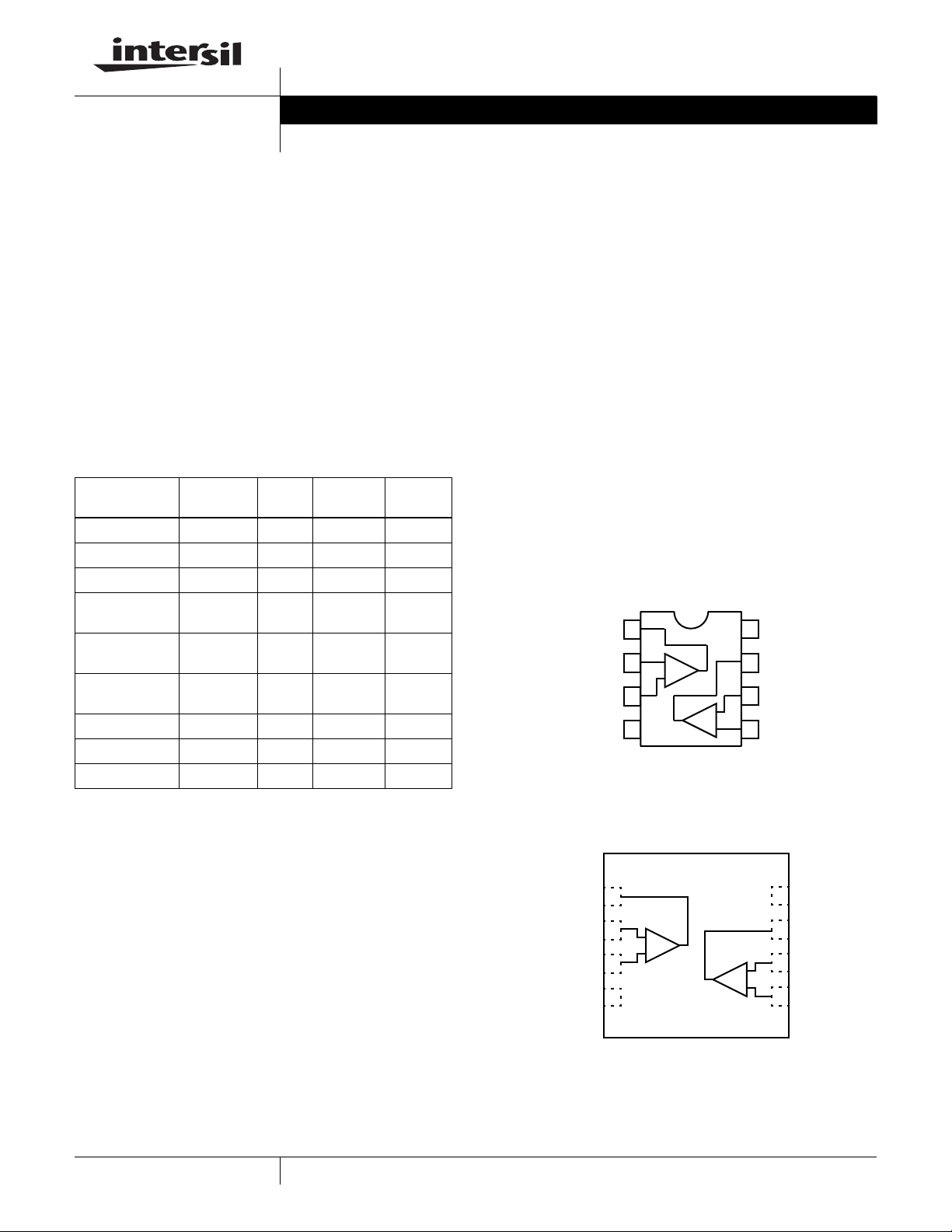
Pinouts
EL1509
(8 LD SOIC)
TOP VIEW
VSOUTA
8
OUTB
7
INB-
6
-
+
INB+
5
VS
8
OUTA
INA-
INA+
GND
1
-
2
+
3
4
EL1509
(8 LD DFN)
TOP VIEW
1
INA-
INA+
GND
1
CAUTION: These devices are sensitive to electrostatic discharge; follow proper IC Handling Procedures.
1-888-INTERSIL or 1-888-468-3774
| Intersil (and design) is a registered trademark of Intersil Americas Inc.
Copyright © Intersil Americas Inc. 2002-2004, 2007. All Rights Reserved.
All other trademarks mentioned are the property of their respective owners.
OUTB
2
-
+
3
AMP A
4
AMP B
7
INB-
6
-
+
INB+
5
www.BDTIC.com/Intersil
EL1509
Absolute Maximum Ratings (T
V
+ Voltage to Ground . . . . . . . . . . . . . . . . . . . . . . -0.3V to +14.6V
S
V
+ Voltage . . . . . . . . . . . . . . . . . . . . . . . . . . . . . . . . . GND to VS+
IN
Current into any Input . . . . . . . . . . . . . . . . . . . . . . . . . . . . . . . . 8mA
Continuous Output Current . . . . . . . . . . . . . . . . . . . . . . . . . . . 75mA
CAUTION: Stresses above those listed in “Absolute Maximum Ratings” may cause permanent damage to the device. This is a stress only rating and operation of the
device at these or any other conditions above those indicated in the operational sections of this specification is not implied.
IMPORTANT NOTE: All parameters having Min/Max specifications are guaranteed. Typical values are for information purposes only. Unless otherwise noted, all tests
are at the specified temperature and are pulsed tests, therefore: TJ = TC = T
Electrical Specifications V
PARAMETER DESCRIPTION CONDITIONS MIN TYP MAX UNIT
AC PERFORMANCE
BW -3dB Bandwidth A
HD Total Harmonic Distortion f = 150kHz, V
dG Differential Gain A
dθ Differential Phase A
SR Slewrate V
DC PERFORMANCE
V
OS
ΔV
OS
R
OL
INPUT CHARACTERISTICS
I
+ Non-Inverting Input Bias Current -5 5 µA
B
- Inverting Input Bias Current -30 30 µA
I
B
ΔI
-I
B
e
N
i
N
OUTPUT CHARACTERISTICS
V
OUT
I
OUT
SUPPLY
V
S
I
S
Offset Voltage -20 20 mV
VOS Mismatch -10 10 mV
Transimpedance V
- Mismatch -30 30 µA
B
Input Noise Voltage 2.8 nV/√Hz
-Input Noise Current 19 pA/√Hz
Loaded Output Swing (single ended) VS = ±6V, RL = 100Ω to GND ±4.8 ±5 V
Output Current RL = 0Ω 450 mA
Supply Voltage Single Supply 5 12 V
Supply Current All Outputs at Mid Supply 14.2 18 mA
= +25°C)
A
Operating Temperature . . . . . . . . . . . . . . . . . . . . . . .-40°C to +85°C
Storage Temperature Range . . . . . . . . . . . . . . . . . .-60°C to +150°C
Operating Junction Temperature . . . . . . . . . . . . . . .-40°C to +150°C
Power Dissipation . . . . . . . . . . . . . . . . . . . . . . . . . . . . . See Curves
A
= +12V, RF = 1.5kΩ, RL = 100Ω connected to mid supply, TA = 25°C, unless otherwise specified.
S
= +4 70 MHz
V
= 16V
O
= +2, RL = 37.5Ω 0.15 %
V
= +2, RL = 37.5Ω 0.1 °
V
from -3V to +3V 350 500 V/µs
OUT
from -4.5V to +4.5V 0.7 1.4 2.5 MΩ
OUT
= ±6V, RL = 25Ω to GND ±4.4 ±4.7 V
V
S
, RL = 25Ω -85 dBc
P-P
2
FN7015.2
March 26, 2007
www.BDTIC.com/Intersil
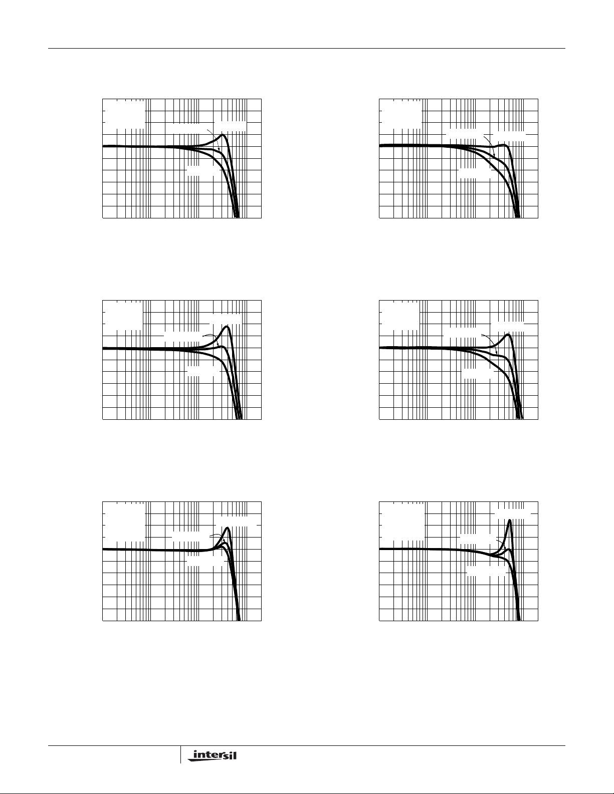
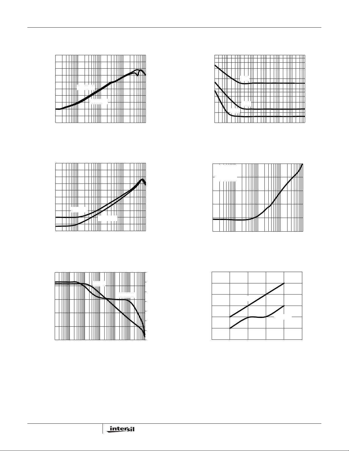
Typical Performance Curves
EL1509
28
AV=10
=±6V
V
S
R
=100Ω
24
L
20
16
GAIN (dB)
12
8
100K 100M1M 10M
FREQUENCY (Hz)
RF=1.5kΩ
RF=1kΩ
RF=2kΩ
FIGURE 1. DIFFERENTIAL FREQUENCY RESPONSE vs RF
(EL1509CS)
22
AV=5
V
=±6V
S
=100Ω
R
18
L
RF=1.5kΩ
14
10
GAIN (dB)
RF=1kΩ
RF=2kΩ
28
AV=10
=±6V
V
S
R
=100Ω
24
L
20
16
GAIN (dB)
12
8
100K 100M1M 10M
RF=1.5kΩ
RF=2kΩ
FREQUENCY (Hz)
RF=1kΩ
FIGURE 2. DIFFERENTIAL FREQUENCY RESPONSE vs RF
(EL1509CL)
22
AV=5
V
=±6V
S
=100Ω
R
18
L
14
10
GAIN (dB)
RF=1.5kΩ
RF=1kΩ
RF=2kΩ
6
2
100K 100M1M 10M
FREQUENCY (Hz)
FIGURE 3. DIFFERENTIAL FREQUENCY RESPONSE vs R
(EL1509CS)
22
AV=5
=±6V
V
S
R
=100Ω
18
L
=1.5kΩ
R
F
14
10
GAIN (dB)
6
2
100K 100M1M 10M
FREQUENCY (Hz)
CL=10pF
CL=22pF
CL=0pF
FIGURE 5. DIFFERENTIAL FREQUENCY RESPONSE vs C
(EL1509CS)
6
2
100K 100M1M 10M
FREQUENCY (Hz)
F
FIGURE 4. DIFFERENTIAL FREQUENCY RESPONSE vs RF
(EL1509CL)
22
AV=5
=±6V
V
S
=100Ω
18
R
L
R
=1.5kΩ
F
14
10
GAIN (dB)
6
2
100K 100M1M 10M
FREQUENCY (Hz)
L
FIGURE 6. DIFFERENTIAL FREQUENCY RESPONSE vs CL
CL=10pF
CL=22pF
CL=0pF
(EL1509CL)
3
FN7015.2
March 26, 2007
www.BDTIC.com/Intersil
Typical Performance Curves
EL1509
55
AV=5
53
R
=1.5kΩ
F
51
=100Ω
R
L
49
47
45
BW (MHz)
43
41
39
37
35
2.5 5 634 5.53.5 4.5
EL1509CL
(V)
±V
S
EL1509CS
-45
VS=±2.5V
-50
A
=5
V
=1.5kΩ
R
F
-55
=100Ω
R
L
f=1MHz
-60
-65
HD (dB)
-70
-75
-80
-85
14.55.51.5 2.5 3.5 534
2
(V)
V
OP-P
HD3
HD2
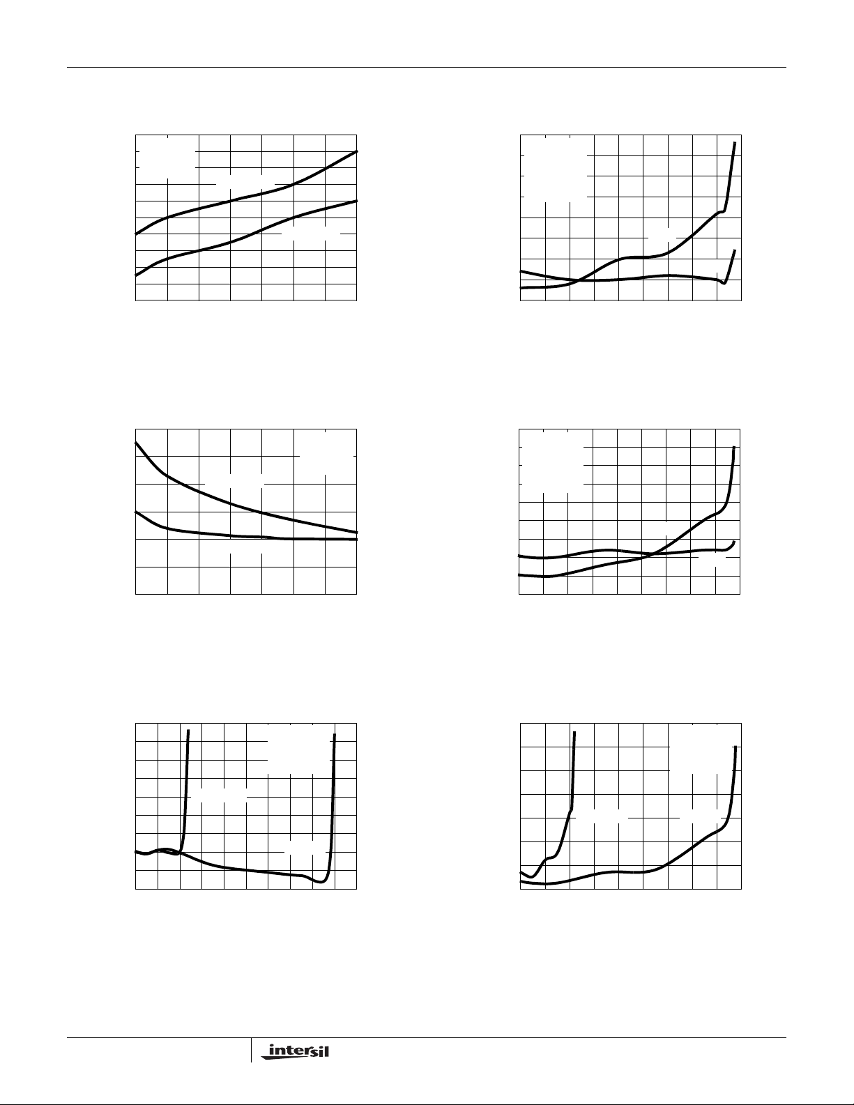
FIGURE 7. DIFFERENTIAL BANDWIDTH vs SUPPLY VOLTAGE FIGURE 8. DIFFERENTIAL HARMONIC DISTORTION vs
DIFFERENTIAL OUTPUT VOLTAGE (ALL
PACKAGES)
4
3
2
1
PEAKING (dB)
0
-1
-2
2.5 633.5 4.5 5.545
EL1509CS
EL1509CL
±V
S
(V)
AV=5
R
F
R
L
=1.5kΩ
=100Ω
-45
-50
-55
-60
-65
-70
HD (dB)
-75
-80
-85
-90
1111935 9 157
VS=±6V
=5
A
V
=1.5kΩ
R
F
R
=100Ω
L
f=1MHz
V
OP-P
HD3
HD2
1713
(V)
FIGURE 9. DIFFERENTIAL PEAKING vs SUPPLY VOLTAGE FIGURE 10. DIFFERENTIAL HARMONIC DISTORTION vs
DIFFERENTIAL OUTPUT VOLTAGE (ALL
PACKAGES)
-45
-50
-55
-60
-65
-70
THD (dB)
-75
-80
-85
-90
1152135 9 19713
VS=±2.5V
V
OP-P
(V)
AV=5
R
=1.5kΩ
F
=100Ω
R
L
f=150kHz
VS=±6V
1711
FIGURE 11. DIFFERENTIAL TOT AL HARMONIC DISTORTION
vs DIFFERENTIAL OUTPUT VOLTAGE (ALL
FIGURE 12. DIFFERENTIAL TOTAL HARMONIC DISTORTION
-45
-50
-55
-60
-65
THD (dB)
-70
-75
-80
115193 7 11 17913
VS=±2.5V VS=±6V
5
V
OP-P
(V)
AV=5V
R
F
R
L
f=1MHz
vs DIFFERENTIAL OUTPUT (ALL PACKAGES)
=1.5kΩ
=100Ω
PACKAGES)
4
March 26, 2007
FN7015.2
www.BDTIC.com/Intersil
Typical Performance Curves
EL1509
-10
-20
-30
-40
-50
-60
-70
-80
ISOLATION (dB)
-90
-100
-110
10K 100K 1M
B → A
A → B
100M10M
FREQUENCY (Hz)
100
IB-
10
E
N
CURRENT NOISE (pA/√Hz)
VOLTAGE NOISE (nV/√Hz),
1
10 10M
IB+
FREQUENCY (Hz)
100M100K 1M10K100 1K
FIGURE 13. CHANNEL ISOLATION vs FREQUENCY FIGURE 14. VOLTAGE AND CURRENT NOISE vs FREQUENCY
30
20
10
0
-10
-20
-30
PSRR (dB)
-40
-50
-60
-70
10K
PSRR-
100K 10M1M
FREQUENCY (Hz)
PSRR+
100M
100
VS=±12V
A
=1
V
=1.5kΩ
R
10
F
1
0.1
0.01
OUTPUT IMPEDANCE (Ω)
0.001
10K 100K 1M 100M
FREQUENCY (Hz)
10M
FIGURE 15. POWER SUPPLY REJECTION vs FREQUENCY FIGURE 16. OUTPUT IMPEDANCE vs FREQUENCY
10M
1M
100K
10K
MAGNITUDE (Ω)
1K
100
100 10K
GAIN
FREQUENCY (Hz)
PHASE
50
0
-50
-100
-150
PHASE (°)
-200
-250
-300
100M1M1K 100K 10M
0.06
0.05
0.04
0.03
0.02
0.01
DIFFERENTIAL GAIN (%),
DIFFERENTIAL PHASE (°)
0
03512 4
GAIN
PHASE
NUMBER OF 150Ω LOADS
FIGURE 17. TRANSIMEDANCE (ROL) vs FREQUENCY FIGURE 18. DIFFERENTIAL GAIN & PHASE
5
FN7015.2
March 26, 2007
www.BDTIC.com/Intersil
Typical Performance Curves
EL1509
14.5
14
13.5
13
SUPPLY CURRENT (mA)
12.5
-50 100 150-25 0 50 12525 75
TEMPERATURE (°C)
10
8
6
4
2
0
-2
-4
-6
INPUT BIAS CURRENT (µA)
-8
-10
-50 100 150-25 0 50 12525 75
IB-
IB+
TEMPERATURE (°C)
FIGURE 19. SUPPLY CURRENT vs TEMPERATURE FIGURE 20. INPUT BIAS CURRENT vs TEMPERATURE
5.2
RL=100Ω
5.15
5.1
50.5
5
4.95
4.9
OUTPUT VOLTAGE (±V)
4.85
4.8
-50 100 150-25 0 50 12525 75
TEMPERATURE (°C)
520
510
500
490
480
470
SLEW RATE (V/µs)
460
450
440
-50 100 150-25 0 50 12525 75
TEMPERATURE (°C)
FIGURE 21. OUTPUT VOLTAGE vs TEMPERATURE FIGURE 22. SLEW RATE vs TEMPERATURE
16
14
12
10
8
(mA)
S
I
6
4
2
0
06712 435
(V)
±V
S
7
6
5
4
3
2
1
0
-1
OFFSET VOLTAGE (mV)
-2
-3
-50 100 150-25 0 50 12525 75
TEMPERATURE (°C)
FIGURE 23. SUPPLY CURRENT vs SUPPLY VOLTAGE FIGURE 24. OFFSET VOLTAGE vs TEMPERATURE
6
FN7015.2
March 26, 2007
www.BDTIC.com/Intersil
EL1509
Typical Performance Curves
JEDEC JESD51-3 AND SEMI G42-88 (SINGLE
LAYER) TEST BOARD
3
2.5
2
1.5
1
0.5
TRANSIMPEDANCE (MΩ)
0
-50 100 150-25 0 50 12525 75
TEMPERATURE (°C)
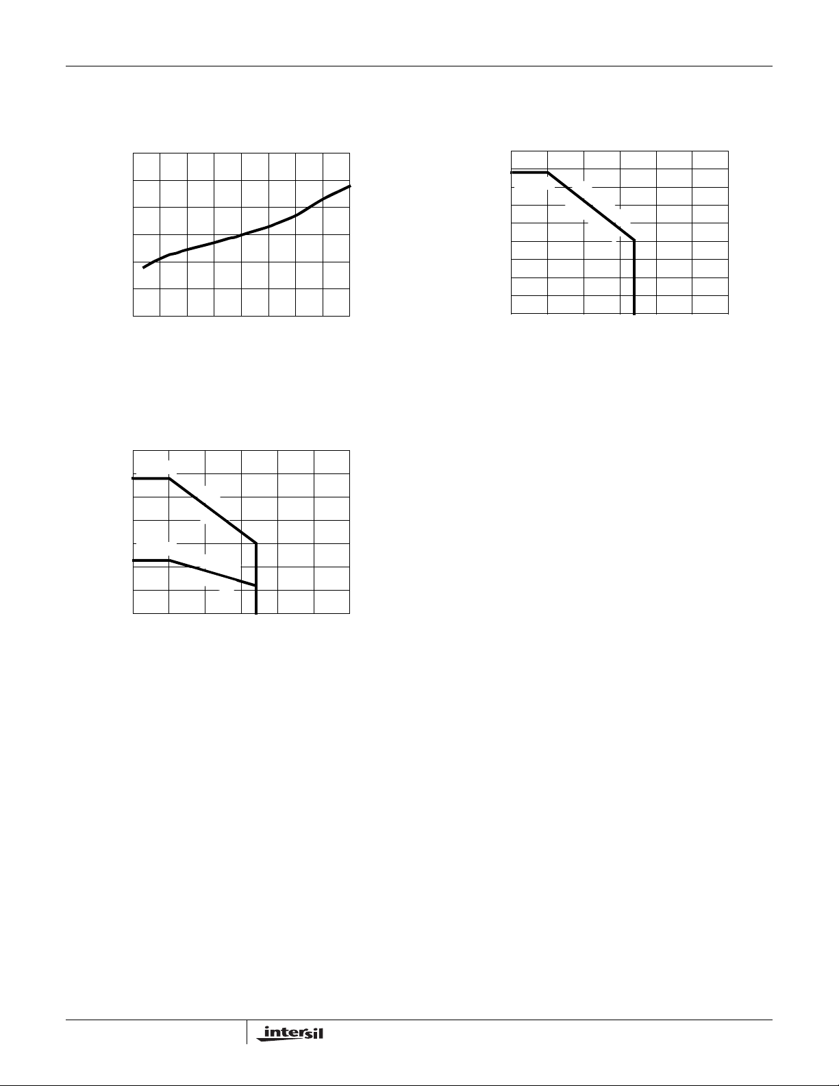
FIGURE 25. TRANSIMEDANCE vs TEMPERATURE FIGURE 26. PACKAGE POWER DISSIP A TION vs AMBIENT
JEDEC JESD51-7 HIGH EFFECTIVE THERMAL
CONDUCTIVITY (4-LAYER) TEST BOARD (DFN EXPOSED
DIEPAD SOLDERED TO PCB PER JESD51-5)
3.5
2.907W
3
2.5
2
1.5
1.136W
1
POWER DISSIPATION (W)
0.5
0
015050 100
D
F
N
4
8
3
°
C
/
W
S
O
8
1
1
0
°
C
/
W
AMBIENT TEMPERATURE (°C)
12525 75 85
0.9
0.8
781mW
0.7
0.6
0.5
0.4
0.3
0.2
POWER DISSIPATION (W)
0.1
0
0 15050 100 12525 75 85
AMBIENT TEMPERATURE (°C)
TEMPERATURE
S
O
8
&
1
D
6
F
0
N
°
C
8
/
W
FIGURE 27. PACKAGE POWER DISSIP A TION vs AMBIENT
TEMPERATURE
Applications Information
Product Description
The EL1509 is a dual operational amplifier designed for
customer premise line driving in DMT ADSL solutions. It is a
dual current mode feedback amplifier with low distortion
while drawing moderately low supply current. It is built using
Elantec's proprietary complimentary bipolar process and is
offered in industry standard pin-outs. Due to the current
feedback architecture, the EL1509 closed-loop 3dB
bandwidth is dependent on the value of the feedback
resistor. First the desired bandwidth is selected by choosing
the feedback resistor, R
the gain resistor, R
Typical Performance Curves section show the effect of
varying both R
and RG. The 3dB bandwidth is somewhat
F
dependent on the power supply voltage.
, and then the gain is set by picking
F
. The curves at the beginning of the
G
7
Power Supply Bypassing and Printed Circuit
Board Layout
As with any high frequency device, good printed circuit
board layout is necessary for optimum performance. Ground
plane construction is highly recommended. Lead lengths
should be as short as possible, below ¼”. The power supply
pins must be well bypassed to reduce the risk of oscillation.
A 1.0µF tantalum capacitor in parallel with a 0.01µF ceramic
capacitor is adequate for each supply pin.
For good AC performance, parasitic capacitances should be
kept to a minimum, especially at the inverting input. This
implies keeping the ground plane away from this pin. Carbon
resistors are acceptable, while use of wire-wound resistors
should not be used because of their parasitic inductance.
Similarly, capacitors should be low inductance for best
performance.
FN7015.2
March 26, 2007
www.BDTIC.com/Intersil
EL1509
Capacitance at the Inverting Input
Due to the topology of the current feedback amplifier, stray
capacitance at the inverting input will affect the AC and
transient performance of the EL1509 when operating in the
non-inverting configuration.
In the inverting gain mode, added capacitance at the
inverting input has little effect since this point is at a virtual
ground and stray capacitance is therefore not “seen” by the
amplifier.
Feedback Resistor Values
The EL1509 has been designed and specified with RF =
1.5kΩ for A
= +5. This value of feedback resistor yields
V
extremely flat frequency response with little to no peaking
out to 50MHz. As is the case with all current feedback
amplifiers, wider bandwidth, at the expense of slight
peaking, can be obtained by reducing the value of the
feedback resistor. Inversely, larger values of feedback
resistor will cause rolloff to occur at a lower frequency. See
the curves in the Typical Performance Curves section which
show 3dB bandwidth and peaking vs. frequency for various
feedback resistors and various supply voltages.
Bandwidth vs Temperature
Whereas many amplifier's supply current and consequently
3dB bandwidth drop off at high temperature, the EL1509 was
designed to have little supply current variations with
temperature. An immediate benefit from this is that the 3dB
bandwidth does not drop off drastically with temperature.
Supply Voltage Range
The EL1509 has been designed to operate with supply
voltages from ±2.5V to ±6V. Optimum bandwidth, slew rate,
and video characteristics are obtained at higher supply
voltages. However, at ±2.5V supplies, the 3dB bandwidth at
A
= +2 is a respectable 40MHz.
V
Single Supply Operation
If a single supply is desired, values from +5V to +12V can be
used as long as the input common mode range is not
exceeded. When using a single supply, be sure to either 1)
DC bias the inputs at an appropriate common mode voltage
and AC couple the signal, or 2) ensure the driving signal is
within the common mode range of the EL1509.
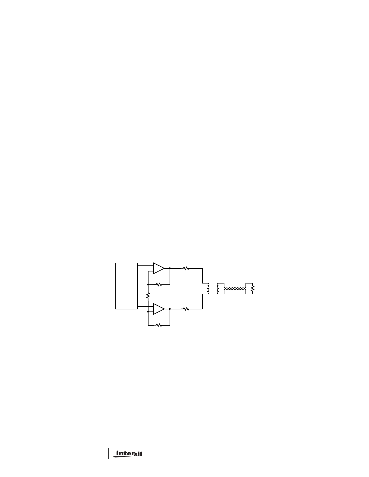
ADSL CPE Applications
The EL1509 is designed as a line driver for ADSL CPE
modems. It is capable of outputting 250mA of output current
with a typical supply voltage headroom of 1.3V. It can
achieve -85dBc of distortion at low 7.1mA of supply current
per amplifier.
The average line power requirement for the ADSL CPE
application is 13dBm (20mW) into a 100Ω line. The average
line voltage is 1.41V
ratio (crest factor) of 5.3 implies peak voltage of 7.5V into the
line. Using a differential drive configuration and transformer
coupling with standard back termination, a transformer ratio
of 1:2 is selected. The circuit configuration is as shown
below.
. The ADSL DMT peak to average
RMS
AFE
+
-
1.5k
464Ω
+
-
1.5k
12.5
TX1
100
1:2
12.5
8
FN7015.2
March 26, 2007
www.BDTIC.com/Intersil
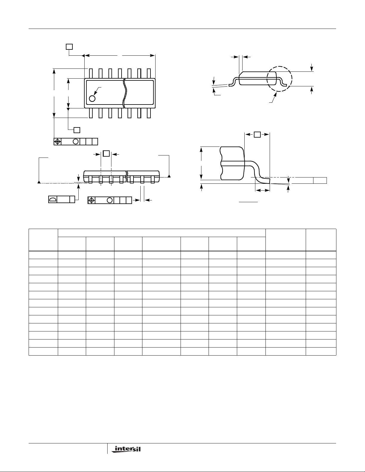
Small Outline Package Family (SO)
A
D
NN
(N/2)+1
EL1509
h X 45°
PIN #1
E
C
SEATING
PLANE
0.004 C
E1
B
0.010 BM CA
I.D. MARK
1
e
0.010 BM CA
(N/2)
c
SEE DETAIL “X”
L1
H
A2
GAUGE
PLANE
A1
b
DETAIL X
L
4° ±4°
MDP0027
SMALL OUTLINE PACKAGE FAMILY (SO)
INCHES
SO16
SYMBOL
A 0.068 0.068 0.068 0.104 0.104 0.104 0.104 MAX -
A1 0.006 0.006 0.006 0.007 0.007 0.007 0.007 ±0.003 A2 0.057 0.057 0.057 0.092 0.092 0.092 0.092 ±0.002 -
b 0.017 0.017 0.017 0.017 0.017 0.017 0.017 ±0.003 -
c 0.009 0.009 0.009 0.011 0.011 0.011 0.011 ±0.001 D 0.193 0.341 0.390 0.406 0.504 0.606 0.704 ±0.004 1, 3
E 0.236 0.236 0.236 0.406 0.406 0.406 0.406 ±0.008 -
E1 0.154 0.154 0.154 0.295 0.295 0.295 0.295 ±0.004 2, 3
e 0.050 0.050 0.050 0.050 0.050 0.050 0.050 Basic L 0.025 0.025 0.025 0.030 0.030 0.030 0.030 ±0.009 -
L1 0.041 0.041 0.041 0.056 0.056 0.056 0.056 Basic -
h 0.013 0.013 0.013 0.020 0.020 0.020 0.020 Reference -
N 8 14 16 16 20 24 28 Reference -
NOTES:
1. Plastic or metal protrusions of 0.006” maximum per side are not included.
2. Plastic interlead protrusions of 0.010” maximum per side are not included.
3. Dimensions “D” and “E1” are measured at Datum Plane “H”.
4. Dimensioning and tolerancing per ASME Y14.5M-1994
(0.150”)
SO16 (0.300”)
(SOL-16)
SO20
(SOL-20)
SO24
(SOL-24)
SO28
(SOL-28)
TOLERANCE NOTESSO-8 SO-14
A
0.010
Rev. M 2/07
9
FN7015.2
March 26, 2007

www.BDTIC.com/Intersil
Dual Flat No-Lead Package Family (DFN)
A
D
NN-1
0.075 C
2X
E
B
4
L1
(E2)
5
C
SEATING
PLANE
(N LEADS
& EXPOSED PAD)
e
0.08 C
PIN #1
I.D.
2
1
TOP VIEW
(D2)
N-1
2
BOTTOM VIEW
0.10
0.075 C
2X
N
(N LEADS)
L
PIN #1 I.D.
1
0.10 C A B
b
C
SEE DETAIL "X"
3
M
EL1509
MDP0047
DUAL FLAT NO-LEAD PACKAGE FAMILY (JEDEC REG: MO-229)
MILLIMETERS
SYMBOL
A 0.85 0.90 ±0.10
A1 0.02 0.02 +0.03/-0.02
b 0.30 0.25 ±0.05
c 0.20 0.20 Reference
D 4.00 3.00 Basic
D2 3.00 2.25 Reference
E 4.00 3.00 Basic
E2 2.20 1.50 Reference
e 0.80 0.50 Basic
L 0.50 0.50 ±0.10
L1 0.10 0 M aximum
NOTES:
1. Dimensioning and tolerancing per ASME Y14.5M-1994.
2. Exposed lead at side of package is a non-functional feature.
3. Bottom-side pin #1 I.D. may be a diepad chamfer, an extended
tiebar tab, or a small square as shown.
4. Exposed leads may extend to the edge of the package or be
pulled back. See dimension “L1”.
5. Inward end of lead may be square or circular in shape with radius
(b/2) as shown.
6. N is the total number of leads on the device.
TOLERANCEDFN8 DFN10
Rev. 2 2/07
2
C
A
(c)
A1
DETAIL X
All Intersil U.S. products are manufactured, assembled and tested utilizing ISO9000 quality systems.
Intersil Corporation’s quality certifications can be viewed at www.intersil.com/design/quality
Intersil products are sold by description only. Intersil Corporation reserves the right to make changes in circuit design, software and/or specifications at any time without
notice. Accordingly, the reader is cautioned to verify that data sheets are current before placing orders. Information furnished by Intersil is believed to be accurate and
reliable. However, no responsibility is assumed by Intersil or its subsidiaries for its use; nor for any infringements of patents or other rights of third parties which may result
from its use. No license is granted by implic atio n or other wise u nde r any p a tent or patent rights of Intersil or it s sub sidi aries.
For information regarding Intersil Corporation and its products, see www.intersil.com
10
FN7015.2
March 26, 2007
 Loading...