

®
www.BDTIC.com/Intersil
EL1508
Data Sheet March 26, 2007
Differential DSL Line Driver
The EL1508 is designed for driving full rate ADSL signals in
both CO and CPE applications at very low power dissipation.
The high drive capability of 450mA makes this driver ideal
for both CAP and DMT designs. It contains two wideband,
high-voltage, current mode feedback amplifiers with a
number of power dissipation reduction features.
These drivers achieve an MTPR distortion measurement of
better than 70dB, while consuming typically 6mA of total
supply current. This supply current can be set using a
resistor on the I
also be used to adjust supply current to one of four pre-set
modes (full-I
EL1508 operates on ±5V to ±12V supplies and retains its
bandwidth and linearity over the complete supply range.
The device is supplied in a thermally-enhanced 20 Ld SOIC
(0.300”), a thermally-enhanced 16 Ld SOIC (0.150”), and the
small footprint (4x5mm) 24 Ld QFN packages. The EL1508
is specified for operation over the full -40°C to +85°C
temperature range.
pin. Two other pins (C0 and C1) can
ADJ
, 2/3-IS, 1/3-IS, and full power-down). The
S
FN7014.5
Features
• 450mA output drive capability
•43.6V
nd/3rd
•2
differential output drive into 100Ω
P-P
harmonics of -85dBc/-75dBc
• MTPR of -70dB
• Operates down to 3mA per amplifier supply current
• Power control features
• Pin-compatible with EL1503
• Pb-free plus anneal available (RoHS compliant)
Applications
• ADSL line driver
• HDSL line driver
• Video distribution amplifier
• Video twisted-pair line driver
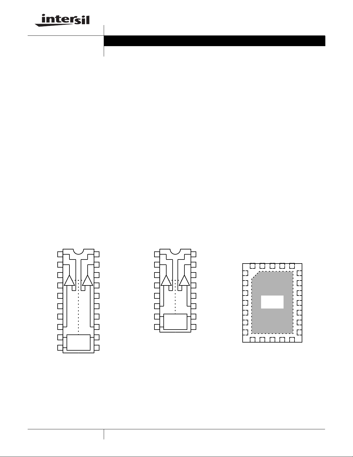
Pinouts
VIN-A
VOUTA
GND*
GND*
GND*
GND*
VIN+A
EL1508
[20 LD SOIC (0.300”)]
TOP VIEW
1
2
3
VS-
C1
C0
4
5
6
7
8
9
10
AB
POWER
CONTROL
LOGIC
EL1508
[16 LD SOIC (0.150”)]
TOP VIEW
VIN-B
20
VOUTB
19
VS+
18
-+ -+
GND*
17
GND*
16
GND*
15
GND*
14
VIN+B
13
IADJ
12
NC
11
*GND PINS ARE HEAT SPREADERS
1
VIN-A
VOUTA
2
VS-
3
GND*
4
GND*
5
VIN+A
6
C1
7
C0
8 9
POWER
CONTROL
LOGIC
VIN-B
16
VOUTB
15
NC
NC
VS-
NC
NC
NC
GND
1
2
3
4
5
6
7
VS+
14
-+ -+
GND*
13
GND*
12
VIN+B
11
IADJ
10
NC
EL1508
(24 LD QFN)
TOP VIEW
VOUTA
VIN-A
24
23
THERMAL
PAD
8
9
C1
VIN+A
NC
22
10
C0
VIN-B
21
11
IADJ
VOUTB
20
19
18
17
16
15
14
13
12
VIN+B
NC
NC
VS+
NC
NC
NC
GND
1
CAUTION: These devices are sensitive to electrostatic discharge; follow proper IC Handling Procedures.
1-888-INTERSIL or 1-888-468-3774
| Intersil (and design) is a registered trademark of Intersil Americas Inc.
Copyright Intersil Americas Inc. 2001-2005, 2007. All Rights Reserved
All other trademarks mentioned are the property of their respective owners.
EL1508
www.BDTIC.com/Intersil
Ordering Information
PART NUMBER PART MARKING TAPE & REEL PACKAGE PKG. DWG. #
EL1508CS EL1508CS - 16 Ld SOIC (0.150”) MDP0027
EL1508CS-T7 EL1508CS 7” 16 Ld SOIC (0.150”) MDP0027
EL1508CS-T13 EL1508CS 13” 16 Ld SOIC (0.150”) MDP0027
EL1508CSZ (See Note) EL1508CSZ - 16 Ld SOIC (0.150”) (Pb-Free) MDP0027
EL1508CSZ-T7 (See Note) EL1508CSZ 7” 16 Ld SOIC (0.150”) (Pb-Free) MDP0027
EL1508CSZ-T13 (See Note) EL1508CSZ 13” 16 Ld SOIC (0.150”) (Pb-Free) MDP0027
EL1508CM EL1508CM - 20 Ld SOIC (0.300”) MDP0027
EL1508CM-T13 EL1508CM 13” 20 Ld SOIC (0.300”) MDP0027
EL1508CMZ (See Note) EL1508CMZ - 20 Ld SOIC (0.300”) (Pb-Free) MDP0027
EL1508CMZ-T13 (See Note) EL1508CMZ 13” 20 Ld SOIC (0.300”) (Pb-Free) MDP0027
EL1508CL 1508CL - 24 Ld QFN MDP0046
EL1508CL-T7 1508CL 7” 24 Ld QFN MDP0046
EL1508CL-T13 1508CL 13” 24 Ld QFN MDP0046
EL1508CLZ (See Note) 1508CLZ - 24 Ld QFN (Pb-Free) MDP0046
EL1508CLZ-T7 (See Note) 1508CLZ 7” 24 Ld QFN (Pb-Free) MDP0046
EL1508CLZ-T13 (See Note) 1508CLZ 13” 24 Ld QFN (Pb-Free) MDP0046
NOTE: Intersil Pb-free plus anneal products employ special Pb-free material sets; molding compounds/die attach materials and 100% matte tin plate
termination finish, which are RoHS compliant and compatible with both SnPb and Pb-free soldering operations. Intersil Pb-free products are MSL
classified at Pb-free peak reflow temperatures that meet or exceed the Pb-free requirements of IPC/JEDEC J STD-020.
2
FN7014.5
March 26, 2007
EL1508
www.BDTIC.com/Intersil
Absolute Maximum Ratings (T
V
+ to VS- Supply Voltage. . . . . . . . . . . . . . . . . . . . . . .-0.3V to 28V
S
+ Voltage to Ground . . . . . . . . . . . . . . . . . . . . . . . . .-0.3V to 28V
V
S
V
- Voltage to Ground. . . . . . . . . . . . . . . . . . . . . . . . . . -28V to 0.3V
S
Driver V
C
0
I
ADJ
CAUTION: Stresses above those listed in “Absolute Maximum Ratings” may cause permanent damage to the device. This is a stress only rating and operation of the
device at these or any other conditions above those indicated in the operational sections of this specification is not implied .
IMPORT ANT NOTE: A ll p arameters having Min/Max specificati ons are gua ranteed. Typ values are for information purposes only. Unless otherwise note d, all test s are at
the specified temperature and are pulsed tests, therefore: T
+ Voltage . . . . . . . . . . . . . . . . . . . . . . . . . . . . . VS- to VS+
IN
, C1 Voltage to GND . . . . . . . . . . . . . . . . . . . . . . . . . . -0.3V to 6V
Voltage to GND . . . . . . . . . . . . . . . . . . . . . . . . . . . . -0.3V to 4V
Electrical Specifications V
= 25°C)
A
= TC = T
J
= ±12V, RF = 2.2kΩ, RL= 65Ω, I
S
A
Current into any Input . . . . . . . . . . . . . . . . . . . . . . . . . . . . . . . . 8mA
Output Current from Driver (Static) . . . . . . . . . . . . . . . . . . . . 100mA
Operating Temperature Range . . . . . . . . . . . . . . . . .-40°C to +85°C
Storage Temperature Range . . . . . . . . . . . . . . . . . .-60°C to +150°C
Operating Junction Temperature . . . . . . . . . . . . . . .-40°C to +150°C
Power Dissipation . . . . . . . . . . . . . . . . . . . . . . . . . . . . . See Curves
= C0 = C1 = 0V, TA = 25°C. Amplifiers tested separately.
ADJL
PARAMETER DESCRIPTION CONDITIONS MIN TYP MAX UNIT
SUPPLY CHARACTERISTICS
+ (Full IS) Positive Supply Current per Amplifier All outputs at 0V, C0 = C1 = 0V 10 14.5 18 mA
I
S
- (Full IS) Negative Supply Current per Amplifier All outputs at 0V, C0 = C1 = 0V -9.5 -13.5 -17.5 mA
I
S
IS+ (2/3 IS) Positive Supply Current per Amplifier All outputs at 0V, C0 = 5V, C1 = 0V 7 10 12.5 mA
- (2/3 IS) Negative Supply Current per Amplifier All outputs at 0V, C0 = 5V, C1 = 0V -6 -9 -12 mA
I
S
+ (1/3 IS) Positive Supply Current per Amplifier All outputs at 0V, C0 = 0V, C1 = 5V 3.75 5.25 7 mA
I
S
- (1/3 IS) Negative Supply Current per Amplifier All outputs at 0V, C0 = 0V, C1 = 5V -2.75 -4.25 -6 mA
I
S
IS+ (6.8k) Positive Supply Current per Amplifier All outputs at 0V, C0 = C1 = 0V,
= 6.8k
R
ADJ
I
- (6.8k) Negative Supply Current per Amplifier All outputs at 0V, C0 = C1 = 0V,
S
+ (Power-down) Positive Supply Current per Amplifier All outputs at 0V, C0 = C1 = 5V 0.75 1.2 2 mA
I
S
- (Power-down) Negative Supply Current per Amplifier All outputs at 0V, C0 = C1 = 5V 0 -0.25 -2 mA
I
S
I
GND
GND Supply Current per Amplifier All outputs at 0V 1 mA
R
= 6.8k
ADJ
33.754.5mA
-3.75 -2.9 -2.25 mA
INPUT CHARACTERISTICS
V
OS
ΔV
OS
+ Non-Inverting Input Bias Current -15 15 µA
I
B
- Inverting Input Bias Current -50 50 µA
I
B
ΔIB-I
R
OL
e
N
i
N
V
IH
V
IL
I
IH1
I
IH0
I
IL
Input Offset Voltage -10 1 10 mV
VOS Mismatch -5 0 5 mV
- Mismatch -25 0 25 µA
B
Transimpedance 1.1 2.9 5 MΩ
Input Noise Voltage 3.5 nV/√Hz
-Input Noise Current 13 pA/√Hz
Input High Voltage C0 and C1 inputs 2.25 V
Input Low Voltage C0 and C1 inputs 0.8 V
Input High Current for C
Input High Current for C
1
0
Input Low Current for C0 or C
1
C1 = 5V 126µA
C0 = 5V 0.5 1 3 µA
C0 = 0V, C1 = 0V -1 1 µA
3
FN7014.5
March 26, 2007
EL1508
www.BDTIC.com/Intersil
Electrical Specifications V
PARAMETER DESCRIPTION CONDITIONS MIN TYP MAX UNIT
OUTPUT CHARACTERISTICS
V
OUT
I
OL
I
OUT
DYNAMIC PERFORMANCE
BW -3 dB Bandwidth A
HD2 2nd Harmonic Distortion f
HD3 3rd Harmonic Distortion f
MTPR Multi-Tone Power Ratio 26kHz to 1.1MHz, R
SR Slewrate V
Loaded Output Swing RL = 100Ω ±10.6 ±10.8 ±11.5 V
Linear Output Current AV = 5, RL = 10Ω, f = 100kHz,
Output Current V
= ±12V, RF = 2.2kΩ, RL= 65Ω, I
S
R
L
THD = -60dBc
OUT
V
= 1MHz, RL = 100Ω, V
C
fC = 1MHz, RL = 25Ω, V
= 1MHz, RL = 100Ω, V
C
= 1MHz, RL = 25Ω, V
f
C
P
LINE
OUT
= C0 = C1 = 0V, TA = 25°C. Amplifiers tested separately. (Continued)
ADJL
= 25Ω ±9.8 ±10.2 ±10.6 V
450 mA
= 1V, RL = 1Ω 1A
= +5 80 MHz
= 2V
OUT
OUT
OUT
OUT
= 100Ω,
= 20.4dBM
from -8V to +8V measured at ±4V 450 600 800 V/µs
LINE
= 2V
= 2V
= 2V
P-P
P-P
P-P
P-P
-90 dBc
-80 dBc
-90 dBc
-75 dBc
-70 dBc
4
FN7014.5
March 26, 2007
Pin Descriptions
www.BDTIC.com/Intersil
EL1508
16 Ld SOIC
(0.150")
1 1 23 VIN-A Channel A Inverting Input
2 2 24 VOUTA Channel A Output (Reference Circuit 1)
3 3 3 VS- Negative Supply
4, 5 4, 5, 6, 7 7 GND Ground Connection
6 8 8 VIN+A Channel A Non-inverting Input
7 9 9 C1 Current Control Bit 1
20 Ld SOIC
(0.300") 24 Ld QFN PIN NAME FUNCTION CIRCUIT
CIRCUIT 1
VS+
VS-
CIRCUIT 2
VS+
8 10 10 C0 Current Control Bit 2 (Reference Circuit 3)
9 11 1, 2, 4, 5, 6, 14,
15, 16, 18, 19, 22
10 12 11 IADJ Supply Current Control Pin
11 13 12 VIN+B Channel B Non-inverting Input (Reference Circuit 2)
12, 13 14, 15, 16, 17 13 GND Ground Connection
14 18 17 VS+ Positive Supply
15 19 20 VOUTB Channel B Output (Reference Circuit 1)
16 20 21 VIN-B Channel B Inverting Input (Reference Circuit 1)
NC Not Connected
I
ADJ
6.7V
CIRCUIT 3
VS+
GND
CIRCUIT 4
5
FN7014.5
March 26, 2007
Typical Performance Curves
www.BDTIC.com/Intersil
EL1508
24
AV=10
V
=±12V
S
=100Ω
R
22
L
R
=0Ω
ADJ
20
18
GAIN (dB)
16
14
100K 1M 10M 100M
RF=2kΩ
RF=2.5kΩ
RF=3kΩ
FREQUENCY (Hz)
RF=1.5kΩ
FIGURE 1. DIFFERENTIAL FREQUENCY RESPONSE vs R
(1/3 POWER MODE)
24
AV=10
=±12V
V
S
R
=100Ω
22
L
=0Ω
R
ADJ
20
18
GAIN (dB)
16
RF=3kΩ
RF=2.5kΩ
RF=1.5kΩRF=2kΩ
18
AV=5
V
=±12V
S
=100Ω
R
16
L
14
12
GAIN (dB)
10
8
100K 1M 10M 100M
F
FIGURE 2. DIFFERENTIAL FREQUENCY RESPONSE
(1/3 POWER MODE)
18
AV=5
V
=±12V
S
=100Ω
R
16
L
14
RF=3.5kΩ
12
GAIN (dB)
10
RF=3kΩ
RF=4kΩ
RF=3.5kΩ
FREQUENCY (Hz)
RF=4kΩ
RF=3kΩ
RF=2kΩ
RF=2.5kΩ
RF=2kΩ
RF=2.5kΩ
14
100K 1M 10M 100M
FREQUENCY (Hz)
FIGURE 3. DIFFERENTIAL FREQUENCY RESPONSE vs R
(2/3 POWER MODE)
24
AV=10
V
=±12V
S
=100Ω
R
22
L
R
=0Ω
ADJ
20
18
GAIN (dB)
16
14
100K 1M 10M 100M
RF=1.5kΩ
RF=2kΩ
RF=2.5kΩ
RF=3kΩ
FREQUENCY (Hz)
FIGURE 5. DIFFERENTIAL FREQUENCY RESPONSE vs R
(FULL POWER MODE)
8
100K 1M 10M 100M
FREQUENCY (Hz)
F
FIGURE 4. DIFFERENTIAL FREQUENCY RESPONSE
(2/3 POWER MODE)
18
AV=5
=±12V
V
S
R
=100Ω
16
L
RF=4kΩ
14
12
GAIN (dB)
10
8
100K 1M 10M 100M
F
FIGURE 6. DIFFERENTIAL FREQUENCY RESPONSE
RF=3kΩ
RF=3.5kΩ
FREQUENCY (Hz)
RF=2kΩ
RF=2.5kΩ
(FULL POWER MODE)
6
FN7014.5
March 26, 2007

Typical Performance Curves (Continued)
www.BDTIC.com/Intersil
EL1508
26
VS=±12V
R
=3kΩ
FB
=5
A
V
22
=83Ω
R
L
R
=0Ω
SET
18
14
MAGNITUDE (dB)
10
6
10K 100K 10M 100M
FREQUENCY (Hz)
100pF
68pF
50pF
22pF
0pF
1M
FIGURE 7. EL1508CM SINGLE-ENDED CONFIGURATION
FREQUENCY RESPONSE vs C
L
(1/3 POWER MODE)
26
VS=±12V
=3kΩ
R
FB
A
=5
22
V
=83Ω
R
L
=0Ω
R
SET
18
14
MAGNITUDE (dB)
10
6
10K 100K 10M 100M
FREQUENCY (Hz)
150pF
100pF
62pF
39pF
22pF
5pF
1M
26
VS=±12V
R
=3kΩ
FB
=5
A
22
V
=83Ω
R
L
R
=0Ω
SET
18
14
MAGNITUDE (dB)
10
6
10K 100K 10M 100M
FREQUENCY (Hz)
150pF
100pF
62pF
39pF
22pF
0pF
1M
FIGURE 8. EL1508CM SINGLE-ENDED CONFIGURATION
FREQUENCY RESPONSE vs C
L
(1/3 POWER MODE)
6
5
4
3
2
PEAKING (dB)
1
0
5678910
TOTAL I
(mA)
S
VS=±12V
R
=3kΩ
FB
=10
A
V
=100Ω
R
L
FIGURE 9. EL1508CM SINGLE-ENDED CONFIGURATION
FREQUENCY RESPONSE vs C
6
VS=±12V
=3kΩ
R
FB
5
=10
A
V
R
=100Ω
L
4
3
2
PEAKING (dB)
1
0
0246810
R
(kΩ)
ADJ
FIGURE 11. PEAKING vs R
L
ADJ
7
FIGURE 10. PEAKING vs IS+
7
6
5
4
3
PEAKING (dB)
2
1
0
5 7 9 11 13 15
(mA)
I
SUPPLY
FIGURE 12. PEAKING vs IS+
VS=±7.5V
=3kΩ
R
FB
A
=10
V
=100Ω
R
L
FN7014.5
March 26, 2007

Typical Performance Curves (Continued)
www.BDTIC.com/Intersil
40
30
(Ω)
20
OUT
R
10
0
10K 100K 1M 100M
FREQUENCY (Hz)
FIGURE 13. OUTPUT IMPEDANCE FIGURE 14. CHANNEL SEPARATION
10M
EL1508
0
-20
-40
-60
GAIN (dB)
-80
-100
10K 100K 10M 100M
A to B
B to A
1M
FREQUENCY (Hz)
100
CURRENT NOISE
10
VOLTAGE NOISE
CURRENT NOISE (pA/√Hz)
VOLTAGE NOISE (nV/√Hz),
1
10 1K 100K
100 10K
FREQUENCY (Hz)
1.4
VS=±12V
=3kΩ
R
FB
1.2
=2
A
V
R
=0Ω
SET
1.0
0.8
0.6
0.4
0.2
DIFFERENTIAL GAIN (%), PHASE (°)
0
1.0 2.0 3.0 4.0
NUMBER of 150Ω RESISTOR LOADS
DIFF GAIN
DIFF PHASE
2.5 3.51.5
FIGURE 15. VOLTAGE AND CURRENT NOISE vs FREQUENCY FIGURE 16. DIFFERENTIAL GAIN/PHASE, F
(2/3 POWER MODE)
0.30
VS=±12V
R
=3kΩ
FB
0.25
=2
A
V
=0Ω
R
SET
0.20
0.15
0.10
0.05
DIFFERENTIAL GAIN (%), PHASE (°)
0
1.0 1.5 2.5 3.5 4.0
2.0 3.0
NUMBER of 150Ω RESISTOR LOADS
DIFF GAIN
DIFF PHASE
0.08
VS=±12V
0.07
R
=3kΩ
FB
=2
A
V
0.06
0.05
0.04
0.03
0.02
0.01
DIFFERENTIAL GAIN (%), PHASE (°)
=0Ω
R
SET
0
12345
NUMBER of 150Ω RESISTOR LOADS
DIFF PHASE
=3.58MHz
O
DIFF GAIN
FIGURE 17. DIFFERENTIAL GAIN/PHASE, F
=3.58MHz
O
FIGURE 18. DIFFERENTIAL GAIN/PHASE, FO=3.58MHz
(2/3 POWER MODE)
8
(FULL POWER MODE)
FN7014.5
March 26, 2007

EL1508
www.BDTIC.com/Intersil
Typical Performance Curves - 24 Ld QFN Package
FREQ=1MHz
-10
=±5V
V
S
R
=0
SET
=100Ω
R
L
GAIN=10
-30
-50
-70
HARMONIC DISTORTION (dB)
-90
1357
024689
V
OUTP-P
HD3
(V)
FIGURE 19. HARMONIC DISTORTION TEST
(1/3 POWER MODE)
0
FREQ=1MHz
-10
V
=±5V
S
=0
R
SET
-20
=100Ω
R
L
GAIN=10
-30
-40
-50
HD (dB)
-60
-70
-80
-90
1357
024689
V
OUTp-p
HD2
(V)
HD2
HD3
0
FREQ=1MHz
=±12V
V
S
R
-20
-40
-60
-80
HARMONIC DISTORTION (dB)
-100
=0
SET
=100Ω
R
L
GAIN=10
HD3
HD2
0 5 10 15 20 25
(V)
V
OUTP-P
FIGURE 20. HARMONIC DISTORTION TEST
(1/3 POWER MODE)
0
FREQ=1MHz
=±12V
V
S
R
-20
-40
-60
-80
HARMONIC DISTORTION (dB)
-100
=0
SET
=100Ω
R
L
GAIN=10
0 5 10 15 20 25
V
OUTP-P
HD3
HD2
(V)
FIGURE 21. HARMONIC DISTORTION TEST
(2/3 POWER MODE)
0
FREQ=1MHz
-10
=±5V
V
S
R
-20
-30
-40
-50
-60
-70
-80
HARMONIC DISTORTION (dB)
-90
-100
=0
SET
=100Ω
R
L
GAIN=10
HD2
024689
V
OUTp-p
5731
(V)
FIGURE 23. HARMONIC DISTORTION TEST
(FULL POWER MODE)
HD3
FIGURE 22. HARMONIC DISTORTION TEST
(2/3 POWER MODE)
0
FREQ=1MHz
=±12V
V
S
R
-20
-40
-60
-80
HARMONIC DISTORTION (dB)
-100
=0
SET
=100Ω
R
L
GAIN=10
0 5 10 15 20 25
V
OUTP-P
HD3
HD2
(V)
FIGURE 24. HARMONIC DISTORTION TEST
(FULL POWER MODE)
9
FN7014.5
March 26, 2007

EL1508
www.BDTIC.com/Intersil
Typical Performance Curves - 20 Ld SOIC (0.300") Package
0
FREQ=1MHz
V
=±5V
S
=0
R
SET
-20
=100Ω
R
L
GAIN=10
-40
HD3
HD2
V
OUTP-P
8
(V)
-60
HARMONIC DISTORTION (dB)
-80
01 9234567
FIGURE 25. HARMONIC DISTORTION vs DIFFERENTIAL
OUTPUT VOLTAGE (1/3 POWER MODE)
FREQ=1MHz
-10
V
=±5V
S
=0
R
SET
=100Ω
R
L
GAIN=10
-30
-50
-70
HARMONIC DISTORTION (dB)
-90
01 92 45678
HD2
3
V
OUTP-P
HD3
(V)
FREQ=1MHz
-10
V
=±12V
S
=0
R
SET
=100Ω
R
L
GAIN=10
-30
-50
-70
HARMONIC DISTORTION (dB)
-90
0 5 10 15 20 25
V
OUTP-P
HD 2
HD 3
(V)
FIGURE 26. HARMONIC DISTORTION vs DIFFERENTIAL
OUTPUT VOLTAGE (1/3 POWER MODE)
FREQ=1MHz
-10
=±12V
V
S
=0
R
SET
R
=100Ω
L
GAIN=10
-30
-50
-70
HARMONIC DISTORTION (dB)
-90
0 5 10 15 20 25
V
OUTP-P
HD 2
HD 3
(V)
FIGURE 27. HARMONIC DISTORTION vs DIFFERENTIAL
OUTPUT VOLTAGE (2/3 POWER MODE)
0
FREQ=1MHz
V
=±5V
S
=0
R
-20
SET
=100Ω
R
L
GAIN=10
-40
-60
-80
HARMONIC DISTORTION (dB)
-100
01 8234567
HD2
V
OUTP-P
HD3
(V)
FIGURE 29. HARMONIC DISTORTION vs DIFFERENTIAL
OUTPUT VOLTAGE (FULL POWER MODE)
FIGURE 28. HARMONIC DISTORTION vs DIFFERENTIAL
OUTPUT VOLTAGE (2/3 POWER MODE)
FREQ=1MHz
-10
=±12V
V
S
R
=0
SET
=100Ω
R
L
GAIN=10
-30
-50
-70
HARMONIC DISTORTION (dB)
-90
0 5 10 15 20 25
V
OUTP-P
HD 2
HD 3
(V)
FIGURE 30. HARMONIC DISTORTION vs DIFFERENTIAL
OUTPUT VOLTAGE (FULL POWER MODE)
10
FN7014.5
March 26, 2007

Typical Performance Curves
www.BDTIC.com/Intersil
EL1508
FREQ=1MHz
=±5V
V
S
-10
R
=6.81kΩ
SET
=100Ω
R
L
GAIN=10
-30
-50
HARMONIC DISTORTION (dB)
-70
HD 3
HD 2
013579
2468
V
(V)
OUTP-P
FIGURE 31. EL1508CM HARMONIC DISTORTION vs
DIFFERENTIAL OUTPUT VOLTAGE
(FULL POWER MODE)
0
FREQ=1MHz
V
=±12V
S
=6.81kΩ
R
SET
-20
=100Ω
R
L
GAIN=10
-40
-60
HARMONIC DISTORTION (dB)
-80
0 5 10 15 20 25
V
OUTP-P
HD 2
HD 3
(V)
FREQ=1MHz
-10
V
=±5V
S
=6.81kΩ
R
SET
=100Ω
R
L
GAIN=10
-30
-50
-70
HARMONIC DISTORTION (dB)
-90
1357
024689
V
OUTP-P
HD3
HD2
(V)
FIGURE 32. EL1508CL HARMONIC DISTORTION TEST
(FULL POWER MODE)
0
FREQ=1MHz
V
=±12V
S
=6.81kΩ
R
-20
SET
=100Ω
R
L
GAIN=10
-40
-60
-80
HARMONIC DISTORTION (dB)
-100
0 5 10 15 20 25
(V)
V
OUTP-P
HD3
HD2
FIGURE 33. EL1508CM HARMONIC DISTORTION vs
DIFFERENTIAL OUTPUT VOLTAGE
(FULL POWER MODE)
V
OUT
C0, C
1
40ns/DIV
2V/DIV
FIGURE 35. DISABLE TIME FIGURE 36. ENABLE TIME
11
FIGURE 34. EL1508CL HARMONIC DISTORTION TEST
(FULL POWER MODE)
V
OUT
C0, C
1
2V/DIV
40ns/DIV
March 26, 2007
FN7014.5

Typical Performance Curves (Continued)
www.BDTIC.com/Intersil
EL1508
21.6
21.4
(V)
P-P
21.2
21.0
FREQ=100kHz
=±12V
20.8
OUTPUT VOLTAGE
20.6
70 110
50 90 130 150 170 190
DIFFERENTIAL LOAD RESISTANCE (Ω)
V
S
R
=0
SET
=10
A
V
FIGURE 37. LOAD RESISTANCE vs OUTPUT VOLTAGE
(ALL POWER MODES)
30
25
20
15
10
SUPPLY CURRENT (mA)
5
0
02 681012
L
U
F
3
/
2
3
/
1
4
SUPPLY VOLTAGE (V)
R
E
W
O
P
L
R
E
W
O
P
R
E
W
O
P
+
-
+
-
+
-
25
21
17
+ (mA)
S
I
13
9
5
0246810
(kΩ)
R
ADJ
FIGURE 38. IS+ vs R
4.5
4.0
3.5
3.0
2.5
2.0
1.5
1.0
POWER DISSIPATION (W)
0.5
0
-40 20-20 60 80
θJA = 30°C/W
θJA = 43°C/W
θJA = 53°C/W
θJA = 80°C/W
0100
AMBIENT TEMPERATURE (°C)
(FULL POWER MODE)
ADJ
40
VS=±12V
=10
R
FB
=10
A
V
R
=100Ω
L
FIGURE 39. SUPPLY CURRENT vs SUPPLY VOLTAGE FIGURE 40. POWER DISSIPATION vs AMBIENT
TEMPERATURE for VARIOUS MOUNTED θ
(See Thermal Resistance Curve on page 15)
USING ELANTEC EL1503CS DEMO BOARD, 2”X2”
(4-LAYER). DEMO BOARD WITH HEATSINK VIA
INTERNAL GROUND PLANE
4
3.5
3
θ
J
A
=
4
7
°
C
/
W
100-40 -20 0 20 40 60
80
POWER DISSIPATION (W)
2.5
2
1.5
1
0.5
0
AMBIENT TEMPERATURE (°C)
FIGURE 41. 16 LD SOIC POWER DISSIPATION and THERMAL
RESISTANCE
FIGURE 42. 24 LD QFN POWER DISSIPATION vs AMBIENT
USING JEDEC JESD51-3 HIGH EFFECTIVE THERMAL
CONDUCTIVITY. (4-LAYER) TEST BOARD, QFN
EXPOSED DIEPAD SOLDERED TO PCB PER JESD51-5
4.0
3.5
POWER DISSIPATION (W)
3.0
2.5
2.0
1.5
1.0
0.5
3.378W
0
θ
J
A
=3
7
°
C
/
W
85
AMBIENT TEMPERATURE (°C)
TEMPERATURE
s
JA
1500 255075100125
12
FN7014.5
March 26, 2007

EL1508
www.BDTIC.com/Intersil
Applications Information
The EL1508 consists of two high-power line driver amplifiers
that can be connected for full duplex differential line
transmission. The amplifiers are designed to be used with
signals up to 4MHz and produce low distortion levels. The
EL1508 has been optimized as a line driver for ADSL CO
application. The driver output stage has been sized to
provide full ADSL CO power level of 20dBM onto the
telephone lines. Realizing that the actual peak output
voltages and currents vary with the line transformer turns
ratio, the EL1508 is designed to support 450mA of output
current which exceeds the level required for 1:2 transformer
ratio. A typical ADSL interface circuit is shown in Figure 43
below. Each amplifier has identical positive gain
connections, and optimum common-mode rejection occurs.
Further, DC input errors are duplicated and create commonmode rather than differential line errors.
DRIVER
INPUT+
DRIVER
INPUT-
RECEIVE
OUT +
AMPLIFIERS
RECEIVE
OUT -
FIGURE 43. TYPICAL LINE INTERFACE CONNECTION
2R
G
RECEIVE
+
R
F
R
F
-
+
R
F
R
-
+
+
-
R
R
F
Input Connections
The EL1508 amplifiers are somewhat sensitive to source
impedance. In particular, they do not like being driven by
inductive sources. More than 100nH of source impedance
can cause ringing or even oscillations. This inductance is
equivalent to about 4” of unshielded wiring, or 6” of
unterminated transmission line. Normal high-frequency
construction obviates any such problem.
Power Supplies and Dissipation
Due to the high power drive capability of the EL1508, much
attention needs to be paid to power dissipation. The power
that needs to be dissipated in the EL1508 has two main
contributors. The first is the quiescent current dissipation.
The second is the dissipation of the output stage.
The quiescent power in the EL1508 is not constant with
varying outputs. In reality, 50% of the total quiescent supply
current needed to power each driver is converted in to output
current. Therefore, in the equation below we should subtract
R
OUT
R
OUT
R
IN
R
IN
LINE +
LINE -
Z
LINE
the average output current, I
lowest. We’ll call this term I
, or 1/2 IQ, whichever is the
O
.
X
Therefore, we can determine a quiescent current with the
equation:
P
DquiescentVSIS21X
–()×=
where:
V
is the supply voltage (VS+ to VS-)
S
IS is the operating supply current (IS+ - IS-) / 2
IX is the lesser of IO or 1/2 I
Q
The dissipation in the output stage has two main
contributors. Firstly, we have the average voltage drop
across the output transistor and secondly, the average
output current. For minimal power dissipation, the user
should select the supply voltage and the line transformer
ratio accordingly. The supply voltage should be kept as low
as possible, while the transformer ratio should be selected
so that the peak voltage required from the EL1508 is close to
the maximum available output swing. There is a trade off,
however, with the selection of transformer ratio. As the ratio
is increased, the receive signal available to the receivers is
reduced.
Once the user has selected the transformer ratio, the
dissipation in the output stages can be selected with the
following equation:
V
S
⎛⎞
P
Dtransistors
2I
-------
–
××=
O
V
O
⎝⎠
2
where:
V
is the supply voltage (VS+ to VS-)
S
VO is the average output voltage per channel
is the average output current per channel
I
O
The overall power dissipation (P
P
Dquiescent
and P
Dtransistor
.
) is obtained by adding
DISS
Estimating Line Driver Power Dissipation in ADSL
CO Applications
Figure 44 on the following page shows a typical ADSL CO
line driver implementation. The average line power
requirement for the ADSL CO application is 20dBM
(100mW) into a 100Ω line. The average line voltage is
3.16V
factor) of 5.3 implies peak voltage of 16.7V into the line.
Using a differential drive configuration and transformer
coupling with standard back termination, a transformer ratio
of 1:1 is selected. With 1:1 transformer ratio, the impedance
across the driver side of the transformer is 100Ω, the
average voltage is 3.16V
31.6mA. The power dissipated in the EL1508 is a
. The ADSL DMT peak to average ratio (crest
RMS
and the average current is
RMA
13
FN7014.5
March 26, 2007

EL1508
www.BDTIC.com/Intersil
combination of the quiescent power and the output stage
power when driving the line:
Pd P
quiescentPoutput-stage
dVSIQVS( 2V
In the full power mode and with 6.8k R
+=
) I
OUT-RMS
××–+×=
OUT-RMS
ADJ
registers, the
EL1508 consumes typically 7mA quiescent current and still
able to maintain very low distortion. The distortion results are
shown in typical performance section of the data sheet.
When driving a load, a large portion (about 50%) of the
quiescent current becomes output load current:
Pd 12 7mA( 50%) 12V( 3.16) 31.6mA 2××–+××=
where:
Pd = 598mW
The θ
requirement needs to be calculated. This is done
JA
using the equation:
Θ
=
JA
T
--------------------------------------------
–
JUNCTTAMB
P
DISS
where:
T
T
P
is the maximum die temperature (150°C)
JUNCT
is the maximum ambient temperature (85°C)
AMB
is the dissipation calculated above
DISS
θJA is the junction to ambient thermal resistance for the
package when mounted on the PCB
150 85–
----------------------
Θ
JA
598mW
108° C/W==
PCB Layout Considerations for QFN and SOIC
Packages
The EL1508 die is packaged in three different thermallyefficient packages: a 20 Ld SOIC (0.300”), a 16 Ld SOIC
(0.150”), and a 24 Ld QFN. The 16 Ld SOIC has the same
external dimensions as a standard 0.150” width SOIC
package, but has the center four lead s ( two p er si de )
internally-fused for heat transfer purposes. Both packages
can use PCB surface metal vias areas and internal ground
planes, to spread heat away from the package. The larger
the PCB area the lower the junction temperature of the
device will be. In XDSL applications, multiple layer circuit
boards with internal ground plane are generally used. 13 mil
vias are recommended to connect the metal area under the
device with the internal ground plane. Examples of the PCB
layouts are shown in the figures below that result in thermal
resistance θ
for the SOIC package. The thermal resistance is obtained
with the EL1508CL and CS demo boards. The demo board
is a 4-layer board built with 2oz. copper and has a dimension
2.
of 4in
guideline to achieve these results. In addition to lower
thermal resistance, the QFN package exhibits much lower
2nd harmonic distortion.
A separate Application Note for the QFN package and layout
recommendations is also available.
of 37°C/W for the QFN package and 47°C/W
JA
Note, the user must follow the thermal layout
+
V
R
S
TX+
FROM
AFE
1.5kΩ
T
FIGURE 44. TYPICAL ADSL CO LINE DRIVER
+
VS-
R
F
2R
X
3k
G
-
V
+
-
V
R
F
3k
IMPLEMENTATION
T
10
0.22µF
TXFR 1:1
+
R
S
T
10
-
S
0.22µF
14
100
TOP (24 LD QFN)
INTERNAL GROUND PLANE (24 LD QFN)
FN7014.5
March 26, 2007

EL1508
www.BDTIC.com/Intersil
TOP (16 Ld SO)
55
50
(°C/W)
JA
45
40
35
MOUNTED DEVICE θ
30
02 10684
FIGURE 45. THERMAL RESISTANCE of 20 LD SO (0.300")
EL1508 vs BOARD COPPER AREA
TOP FOIL ONLY-WITH SOLDER MASK
TOP FOIL ONLY-NO SOLDER MASK
AREA OF CIRCUIT BOARD HEAT SINK (in
Note: 2OZ COPPER USED
TOP FOIL-WITH 0.45in2
BOTTOM FOIL WITH MANY
FEEDTHROUGHS
2
)
Power Control Function
The EL1508 contains two forms of power control operation.
Two digital inputs, C
supply current of the EL1508 drive amplifiers. As the supply
current is reduced, the EL1508 will start to exhibit slightly
higher levels of distortion and the frequency response will be
limited. The 4 power modes of the EL1508 are set up as
shown in the following table:
and C1, can be used to control the
0
INTERNAL GROUND PLANE (16 Ld SO)
EL1508CM PCB Layout Considerations
The 20 Ld SOIC (0.300") Power Package is designed so that
heat may be conducted away from the device in an efficient
manner. To disperse this heat, the center four leads on either
side of the package are internally fused to the mounting
platform of the die. Heat flows through the leads into the
circuit board copper, then spreads and convects to air . Thus,
the ground plane on the component side of the board
becomes the heatsink. This has proven to be a very effective
technique, but several aspects of board layout should be
noted. First, the heat should not be shunted to internal
copper layers of the board nor backside foil, since the
feedthroughs and fiberglass of the board are not very
thermally conductive. To obtain the best thermal resistance
of the mounted part, θ
should have as much area as possible and be as thick as
practical. If possible, the solder mask should be cut away
from the EL1508 to improve thermal resistance. Finally,
metal heatsinks can be placed against the board close to the
part to draw heat toward the chassis. The graph below
shows various θ
JA
copper foil areas.
, the topside copper ground plane
JA
s for the 20 Ld SOIC mounted on different
TABLE 1. POWER MODES OF THE EL1508
C
1
00I
0 1 2/3 IS power mode
1 0 1/3 I
1 1 Power-down
C
0
full power mode
S
power mode
S
OPERATION
Another method for controlling the power consumption of the
EL1508 is to connect a resistor from the I
When the I
pin is grounded (the normal state), the supply
ADJ
pin to ground.
ADJ
current per channel is as per the specifications table on page
2. When a resistor is inserted, the supply current is scaled
according to the “R
vs IS” graphs in the Performance
SET
Curves section.
Both methods of power control can be used simultaneously.
In this case, positive and negative supply currents (per amp)
are given by the equations below:
12.4mA
IS+0.9mA
------------------------------------------------------
IS-
1R
------------------------------------------------------
1R
12.4mA
1574Ω÷+()
SET
1574Ω÷+()
SET
( 1/3C0)+×=
2/3C
1/3C
+()×+=
2/3C
1
1
0
Output Loading
While the drive amplifiers can output in excess of 500mA
transiently, the internal metallization is not designed to carry
more than 100mA of steady DC current and there is no
15
FN7014.5
March 26, 2007

EL1508
www.BDTIC.com/Intersil
current-limit mechanism. This allows safely driving rms
sinusoidal currents of 2 x 100mA, or 200mA. This current is
more than that required to drive line impedances to large
output levels, but output short circuits cannot be tolerated.
The series output resistor will usually limit currents to safe
values in the event of line shorts. Driving lines with no series
resistor is a serious hazard.
The amplifiers are sensitive to capacitive loading. More than
25pF will cause peaking of the frequency response. The
same is true of badly terminated lines connected without a
series matching resistor.
Output AC Coupling
When in power-down mode, several volts of differential
voltage may appear across the line driver outputs. If DC
current path exists between the two outputs, large DC
current can flow from the positive supply rail to the negative
supply rail through the outputs. To avoid DC current flow , the
most effective solution is to place DC blocking capacitors in
series at the outputs, as shown by the 0.22µF capacitors in
Figure 44.
Power Supplies
The power supplies should be well bypassed close to the
EL1508. A 2.2µF tantalum capacitor and a 0.1µF ceramic
capacitor for each supply works well. Since the load currents
are differential, they should not travel through the board
copper and set up ground loops that can return to amplifier
inputs. Due to the class AB output stage design, these
currents have heavy harmonic content. If the ground
terminal of the positive and negative bypass capacitors are
connected to each other directly and then returned to circuit
ground, no such ground loops will occur. This scheme is
employed in the layout of the EL1508 demonstration board,
and documentation can be obtained from the factory.
Single Supply Operation
The EL1508 can also be powered from a single supply
voltage. When operating in this mode, the GND pins can still
be connected directly to GND. To calculate power
dissipation, the equations in the previous section should be
used, with V
equal to half the supply rail.
S
Feedback Resistor Value
The bandwidth and peaking of the amplifiers varies with
supply voltage somewhat and with gain settings. The
feedback resistor values can be adjusted to produce an
optimal frequency response. Here is a series of resistor
values that produce an optimal driver frequency response
(1dB peaking) for different supply voltages and gains:
TABLE 2. OPTIMUM DRIVER FEEDBACK RESISTOR FOR
SUPPLY
VOLTAGE
VARIOUS GAINS AND SUPPLY VOLTAGES
DRIVER VOLTAGE GAIN
2.5 5 10
±5V 3.5k 3.25k 3k
±12V 3.5k 3.25k 3k
All Intersil U.S. products are manufactured, assembled and tested utilizing ISO9000 quality systems.
Intersil Corporation’s quality certifications can be viewed at www.intersil.com/design/quality
Intersil products are sold by description only. Intersil Corporation reserves the right to make changes in circuit design, software and/or specifications at any time without
notice. Accordingly, the reader is cautioned to verify that data sheets are current before placing orders. Information furnished by Intersil is believed to be accurate and
reliable. However, no responsibility is assumed by Intersil or its subsidiaries for its use; nor for any infringements of patents or other rights of third parties which may result
from its use. No license is granted by implic atio n or other wise u nde r any p a tent or patent rights of Intersil or its subsidiaries.
For information regarding Intersil Corporation and its products, see www.intersil.com
16
FN7014.5
March 26, 2007

Small Outline Package Family (SO)
www.BDTIC.com/Intersil
A
D
NN
(N/2)+1
EL1508
h X 45°
PIN #1
E
C
SEATING
PLANE
0.004 C
E1
B
0.010 BM CA
I.D. MARK
1
e
0.010 BM CA
(N/2)
c
SEE DETAIL “X”
L1
H
A2
GAUGE
PLANE
A1
b
DETAIL X
L
4° ±4°
MDP0027
SMALL OUTLINE PACKAGE FAMILY (SO)
INCHES
SO16
SYMBOL
A 0.068 0.068 0.068 0.104 0.104 0.104 0.104 MAX -
A1 0.006 0.006 0.006 0.007 0.007 0.007 0.007 ±0.003 A2 0.057 0.057 0.057 0.092 0.092 0.092 0.092 ±0.002 -
b 0.017 0.017 0.017 0.017 0.017 0.017 0.017 ±0.003 c 0.009 0.009 0.009 0.011 0.011 0.011 0.011 ±0.001 -
D 0.193 0.341 0.390 0.406 0.504 0.606 0.704 ±0.004 1, 3
E 0.236 0.236 0.236 0.406 0.406 0.406 0.406 ±0.008 -
E1 0.154 0.154 0.154 0.295 0.295 0.295 0.295 ±0.004 2, 3
e 0.050 0.050 0.050 0.050 0.050 0.050 0.050 Basic L 0.025 0.025 0.025 0.030 0.030 0.030 0.030 ±0.009 -
L1 0.041 0.041 0.041 0.056 0.056 0.056 0.056 Basic -
h 0.013 0.013 0.013 0.020 0.020 0.020 0.020 Reference -
N 8 14 16 16 20 24 28 Reference -
NOTES:
1. Plastic or metal protrusions of 0.006” maximum per side are not included.
2. Plastic interlead protrusions of 0.010” maximum per side are not included.
3. Dimensions “D” and “E1” are measured at Datum Plane “H”.
4. Dimensioning and tolerancing per ASME Y14.5M-1994
(0.150”)
SO16 (0.300”)
(SOL-16)
SO20
(SOL-20)
SO24
(SOL-24)
SO28
(SOL-28)
TOLERANCE NOTESSO-8 SO-14
A
0.010
Rev. M 2/07
17
FN7014.5
March 26, 2007

EL1508
www.BDTIC.com/Intersil
QFN (Quad Flat No-Lead) Package Family
A
1
2
3
2X
0.075 C
L
(E2)
C
SEATING
PLANE
0.08 C
N LEADS
& EXPOSED PAD
A
C
N
(N-2)
(N-1)
PIN #1
I.D. MARK
TOP VIEW
0.10 BAMC
b
N LEADS
(N/2)
BOTTOM VIEW
e
SIDE VIEW
(c)
A1
DETAIL X
D
(N/2)
(N-2)
(N-1)
N
(D2)
0.10
SEE DETAIL "X"
2
(L)
N LEADS
0.075
PIN #1 I.D.
1
2
3
NE
7
C
2X
B
E
C
3
5
MDP0046
QFN (QUAD FLAT NO-LEAD) PACKAGE FAMILY
(COMPLIANT TO JEDEC MO-220)
MILLIMETERS
SYMBOL
A 0.90 0.90 0.90 0.90 ±0.10 -
A1 0.02 0.02 0.02 0.02 +0.03/-0.02 -
b 0.25 0.25 0.23 0.22 ±0.02 c 0.20 0.20 0.20 0.20 Reference -
D 7.00 5.00 8.00 5.00 Basic -
D2 5.10 3.80 5.80 3.60/2.48 Reference 8
E 7.00 7.00 8.00 6.00 Basic -
E2 5.10 5.80 5.80 4.60/3.40 Reference 8
e 0.50 0.50 0.80 0.50 Basic L 0.55 0.40 0.53 0.50 ±0.05 -
N 44 38 32 32 Reference 4
ND 11 7 8 7 Reference 6
NE 11 12 8 9 Reference 5
MILLIMETERS
SYMBOL
A 0.90 0.90 0.90 0.90 0.90 ±0.10 -
A1 0.02 0.02 0.02 0.02 0.02 +0.03/
b 0.25 0.25 0.30 0.25 0.33 ±0.02 c 0.20 0.20 0.20 0.20 0.20 Reference -
D 4.00 4.00 5.00 4.00 4.00 Basic -
D2 2.65 2.80 3.70 2.70 2.40 Reference -
E 5.00 5.00 5.00 4.00 4.00 Basic -
E2 3.65 3.80 3.70 2.70 2.40 Reference -
e 0.50 0.50 0.65 0.50 0.65 Basic L 0.40 0.40 0.40 0.40 0.60 ±0.05 -
N 28 24 20 20 16 Reference 4
ND 6 5 5 5 4 Reference 6
NE 8 7 5 5 4 Reference 5
NOTES:
1. Dimensioning and tolerancing per ASME Y14.5M-1994.
2. Tiebar view shown is a non-functional feature.
3. Bottom-side pin #1 I.D. is a diepad chamfer as shown.
4. N is the total number of terminals on the device.
5. NE is the number of terminals on the “E” side of the package
(or Y-direction).
6. ND is the number of terminals on the “D” side of the package
(or X-direction). ND = (N/2)-NE.
7. Inward end of terminal may be square or circular in shape with radius
(b/2) as shown.
8. If two values are listed, multiple exposed pad options are available.
Refer to device-specific datasheet.
TOLERANCE NOTESQFN44 QFN3 QFN32
TOLER-
ANCE NOTESQFN28 QFN2 QFN20 QFN16
-0.02
Rev 11 2/07
-
18
FN7014.5
March 26, 2007
 Loading...