

Page 1
www.BDTIC.com/Intersil
®
EL1503A
Data Sheet March 26, 2007
High Power Differential Line Driver
The EL1503A ADSL Line Driver contains two wideband
high-voltage drivers which are ideally suited for both ADSL
and HDSL2 applications. They can supply a 39.2V
into a 22Ω load while exhibiting very low distortion. The
EL1503A also has a number of power saving features. The
I
pin can be used to set the maximum supply current and
ADJ
the C
and C1 pins can be used to digitally vary the supply
0
current to one of four modes. These modes include full
power, low power, terminate only and power down.
The EL1503A uses current-feedback type amplifiers, which
achieve a high slew rate while consuming moderate power.
They retain their frequency response over a wide range of
externally set gains. The EL1503A operates on ±5V to ±12V
supplies and consumes only 12.5mA per amplifier.
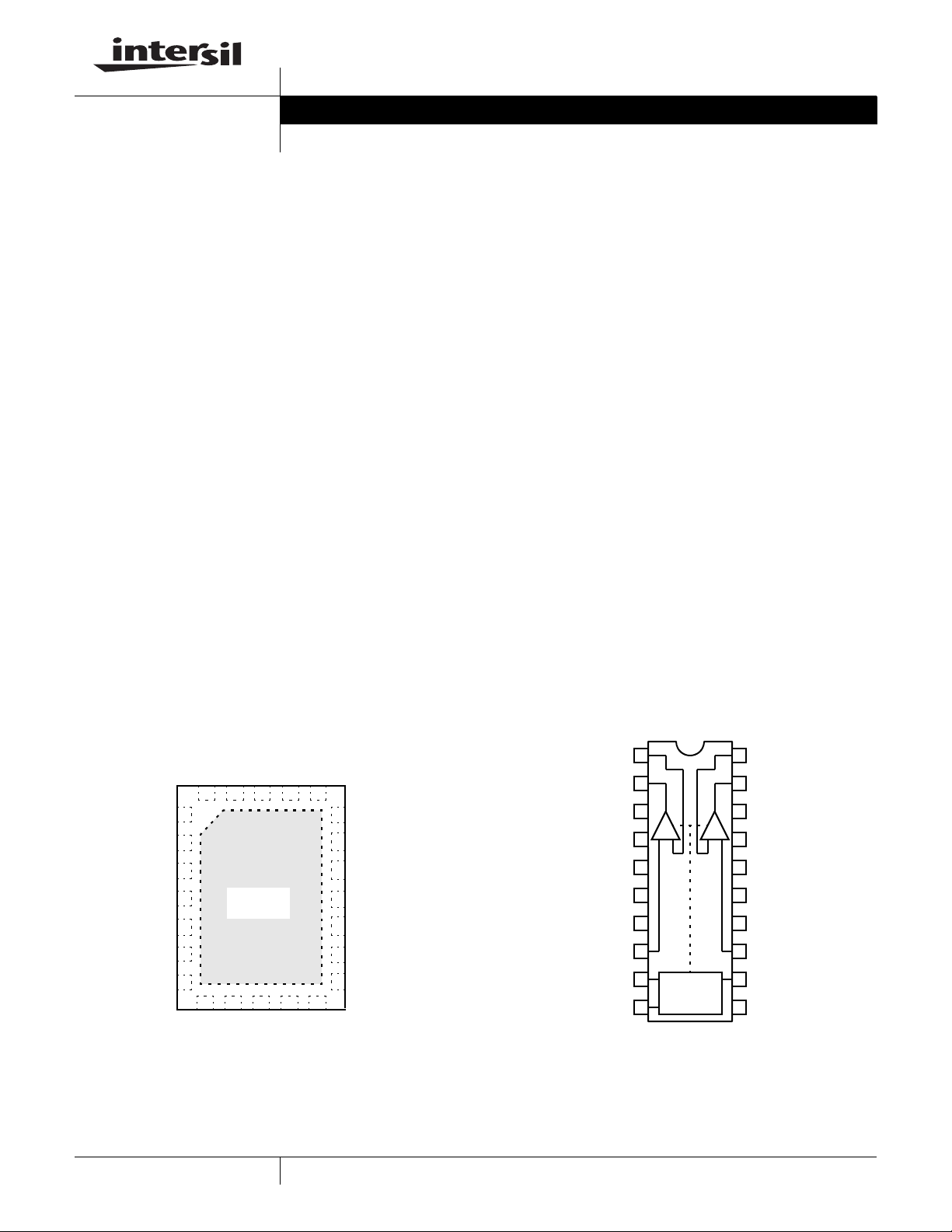
The device is supplied in a thermally-enhanced 20 Ld SOIC
(0.300”) and the small footprint (4x5mm) 24 Ld QFN
packages. Center pins on each side of the 20 Ld and 16 Ld
packages are used as ground connections and heat
spreaders. The QFN package has the potential for a low
(<40°C/W) and dissipates heat by means of a thermal pad
that is soldered onto the PCB. All package options are
specified for operation over the full -40°C to +85°C
temperature range.
P-P
signal
θ
JA
FN7039.2
Features
• High power ADSL driver
•39.2V
•42.4V
• Driver 2
-66dBc/-72dBc at 2V
differential output drive into 22Ω
P-P
differential output drive into 65Ω
P-P
nd/3rd
harmonics of
into 100Ω differential
P-P
• Supply current of 12.5mA per amplifier
• Supply current control
• Power saving modes
• Standard surface-mount packages
• Ultra-small QFN package
• Pb-free plus anneal available (RoHS compliant)
Applications
• ADSL line drivers
• HDSL2 line drivers
• Video distribution amplifiers
Pinouts
NC
NC
VS-
NC
NC
NC
GND
1
2
3
4
5
6
7
EL1503A
(24 LD QFN)
TOP VIEW
VOUTA
VIN-A
24
23
THERMAL
PAD
8
9
C1
VIN+A
NC
22
10
C0
EL1503A
[20 LD SOIC (0.300”)]
TOP VIEW
1
VIN-A
VIN-B
VOUTB
21
20
NC
19
18
NC
17
VS+
NC
16
15
NC
NC
14
13
GND
11
12
IADJ
VIN+B
2
VOUTA
VS-
3
A
GND*
4
GND*
5
GND*
6
GND*
7
VIN+A
8
9
10
POWER
CONTROL
LOGIC
C1
C0
*GND pins are heat spreaders
VIN-B
20
VOUTB
19
VS+
18
B
-+ -+
GND*
17
GND*
16
GND*
15
GND*
14
VIN+B
13
IADJ
12
NC
11
1
CAUTION: These devices are sensitive to electrostatic discharge; follow proper IC Handling Procedures.
1-888-INTERSIL or 1-888-468-3774
| Intersil (and design) is a registered trademark of Intersil Americas Inc.
Copyright Intersil Americas Inc. 2002, 2003, 2005, 2007. All Rights Reserved
All other trademarks mentioned are the property of their respective owners.
Page 2
www.BDTIC.com/Intersil
EL1503A
Ordering Information
PART NUMBER PART MARKING TAPE & REEL PACKAGE PKG. DWG. #
EL1503ACM EL1503ACM - 20 Ld SOIC (0.300") MDP0027
EL1503ACM-T13 EL1503ACM 13” 20 Ld SOIC (0.300") MDP0027
EL1503ACMZ (See Note) EL1503ACMZ - 20 Ld SOIC (0.300") (Pb-Free) MDP0027
EL1503ACMZ-T13 (See Note) EL1503ACMZ 13” 20 Ld SOIC (0.300") (Pb-Free) MDP0027
EL1503ACL 1503ACL - 24 Ld QFN MDP0046
EL1503ACL-T7 1503ACL 7” 24 Ld QFN MDP0046
EL1503ACL-T13 1503ACL 13” 24 Ld QFN MDP0046
EL1503ACLZ (See Note) 1503ACLZ - 24 Ld QFN (Pb-Free) MDP0046
EL1503ACLZ-T7 (See Note) 1503ACLZ 7” 24 Ld QFN (Pb-Free) MDP0046
EL1503ACLZ-T13 (See Note) 1503ACLZ 13” 24 Ld QFN (Pb-Free) MDP0046
NOTE: Intersil Pb-free plus anneal products employ special Pb-free material sets; molding compounds/die attach materials and 100% matte tin plate
termination finish, which are RoHS compliant and compatible with both SnPb and Pb-free soldering operations. Intersil Pb-free products are MSL
classified at Pb-free peak reflow temperatures that meet or exceed the Pb-free requirements of IPC/JEDEC J STD-020.
2
FN7039.2
March 26, 2007
Page 3
www.BDTIC.com/Intersil
EL1503A
s
Absolute Maximum Ratings (T
V
+ to VS- Supply Voltage. . . . . . . . . . . . . . . . . . . . . . . . . . . . . .28V
S
V
+ Voltage to Ground . . . . . . . . . . . . . . . . . . . . . . . .-0.3V to +28V
S
- Voltage to Ground. . . . . . . . . . . . . . . . . . . . . . . . . .-28V to 0.3V
V
S
Input C
Driver V
CAUTION: Stresses above those listed in “Absolute Maximum Ratings” may cause permanent damage to the device. This is a stress only rating and operation of the
device at these or any other conditions above those indicated in the operational sections of this specification is not implied.
IMPORTANT NOTE: All parameters having Min/Max specifications are guaranteed. Typical values are for information purposes only. Unless otherwise noted, all tests
are at the specified temperature and are pulsed tests, therefore: TJ = TC = T
to Ground. . . . . . . . . . . . . . . . . . . . . . . . . .-0.3V to +7V
0/C1
+ Voltage . . . . . . . . . . . . . . . . . . . . . . . . . . . . . VS- to VS+
IN
= +25°C)
A
Current into any Input . . . . . . . . . . . . . . . . . . . . . . . . . . . . . . . . 8mA
Output Current from Driver (static) . . . . . . . . . . . . . . . . . . . . 100mA
Operating Temperature Range . . . . . . . . . . . . . . . . .-40°C to +85°C
Storage Temperature Range . . . . . . . . . . . . . . . . . .-60°C to +150°C
Operating Junction Temperature . . . . . . . . . . . . . . .-40°C to +150°C
Power Dissipation . . . . . . . . . . . . . . . . . . . . . . . . . . . . . See Curves
A
Electrical Specifications V
= ±12V, RF = 1.5kΩ, RL= 65Ω, I
S
= C0 = C1 = 0V, TA = +25°C. Amplifiers tested separately.
ADJ
PARAMETER DESCRIPTION CONDITIONS MIN TYP MAX UNIT
SUPPLY CHARACTERISTICS
I
S+(Full Power)
I
S-(Full Power)
IS+
(Low Power)
I
S-(Low Power)
I
S+(Terminate)
I
S-(Terminate)
IS+
(Power Down)
I
S-(Power Down)
I
GND
Positive Supply Current per Amplifier All outputs at 0V, C0 = C1 = 0V 10 12.5 16 mA
Negative Supply Current per Amplifier All outputs at 0V, C0 = C1 = 0V -15 -11.5 -9 mA
Positive Supply Current per Amplifier All outputs at 0V, C0 = 5V, C1 = 0V 7 9 11.5 mA
Negative Supply Current per Amplifier All outputs at 0V, C0 =5V, C1 = 0V -10.5 -8 -6 mA
Positive Supply Current per Amplifier All outputs at 0V, C0 = 0V, C1 = 5V 4 5.1 7 mA
Negative Supply Current per Amplifier All outputs at 0V, C0 = 0V, C1 = 5V -6 -4 -3 mA
Positive Supply Current per Amplifier All outputs at 0V, C0 = C1 = 5V 0.75 1.05 1.7 mA
Negative Supply Current per Amplifier All outputs at 0V, C0 = C1 = 5V -0.5 -0.25 0.07 mA
GND Supply Current per Amplifier All outputs at 0V -1 mA
INPUT CHARACTERISTICS
V
ΔV
OS
OS
Input Offset Voltage -30 30 mV
VOS Mismatch -15 15 mV
IB+ Non-Inverting Input Bias Current -15 15 µA
- Inverting Input Bias Current -50 50 µA
I
B
-I
ΔI
B
R
OL
e
N
i
N
V
IH
V
IL
I
IH1
I
IH0
I
IL
- Mismatch -30 30 µA
B
Transimpedance 0.4 0.8 MΩ
Input Noise Voltage 3.5 nV/√Hz
-Input Noise Current 13 pA/√Hz
Input High Voltage C0 & C1 inputs 2.7 V
Input Low Voltage C0 & C1 inputs 0.8 V
Input High Current for C
Input High Current for C
1
0
Input Low Current for C1or C
0
C1 = 5V 1.5 8 µA
C0 = 5V 0.75 4 µA
C1 = 0V, C0 = 0V -1 1 µA
OUTPUT CHARACTERISTICS
V
I
OL
I
OUT
OUT
Loaded Output Swing RL = 65Ω ±10.3 ±10.6 V
= 22Ω ±9.3 ±9.8 V
R
L
Linear Output Current AV = 5, RL = 10Ω, f = 100kHz,
450 mA
THD = --60dBc
Output Current V
= 1V, RL = 1Ω 1A
OUT
3
FN7039.2
March 26, 2007
Page 4
www.BDTIC.com/Intersil
EL1503A
Electrical Specifications V
= ±12V, RF = 1.5kΩ, RL= 65Ω, I
S
= C0 = C1 = 0V, TA = +25°C. Amplifiers tested separately. (Continued)
ADJ
PARAMETER DESCRIPTION CONDITIONS MIN TYP MAX UNIT
DYNAMIC PERFORMANCE
BW -3dB Bandwidth A
HD2 2nd Harmonic Distortion f
HD3 3rd Harmonic Distortion f
SR Slewrate V
= +5 80 MHz
V
= 1MHz, RL = 100Ω, V
C
= 1MHz, RL = 25Ω, V
f
C
= 1MHz, RL = 100Ω, V
C
= 1MHz, RL = 25Ω, V
f
C
from -8V to +8V Measured at ±4V 700 1100 V/µs
OUT
OUT
OUT
OUT
OUT
= 2V
= 2V
= 2V
= 2V
P-P
P-P
P-P
P-P
-76 dBc
-72 dBc
-76 dBc
-72 dBc
Typical Performance Curves
25
VS=±12V
=10
A
V
=100Ω
R
L
20
GAIN (dB)
15
100K
1M 100M
RF=1.5kΩ
RF=1.82kΩ
RF=2.0kΩ
RF=2.43kΩ
RF=2.74kΩ
FREQUENCY (Hz)
RF=1.3kΩ
10M
25
VS=±5V
A
=10
V
=100Ω
R
L
20
GAIN (dB)
15
100K
1M 100M
RF=1.5kΩ
RF=1.82kΩ
RF=2.0kΩ
RF=2.4kΩ
RF=2.74kΩ
FREQUENCY (Hz)
RF=1.3kΩ
10M
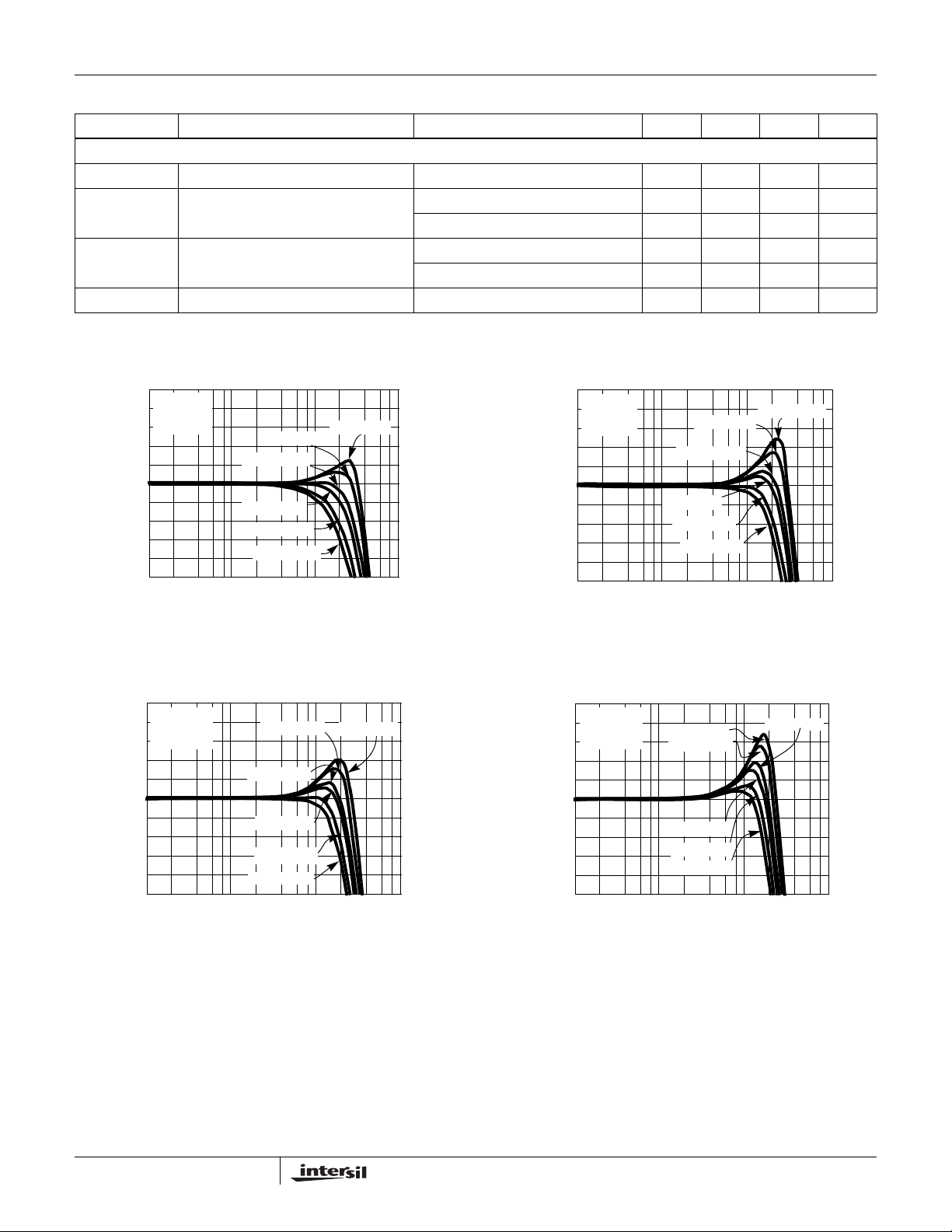
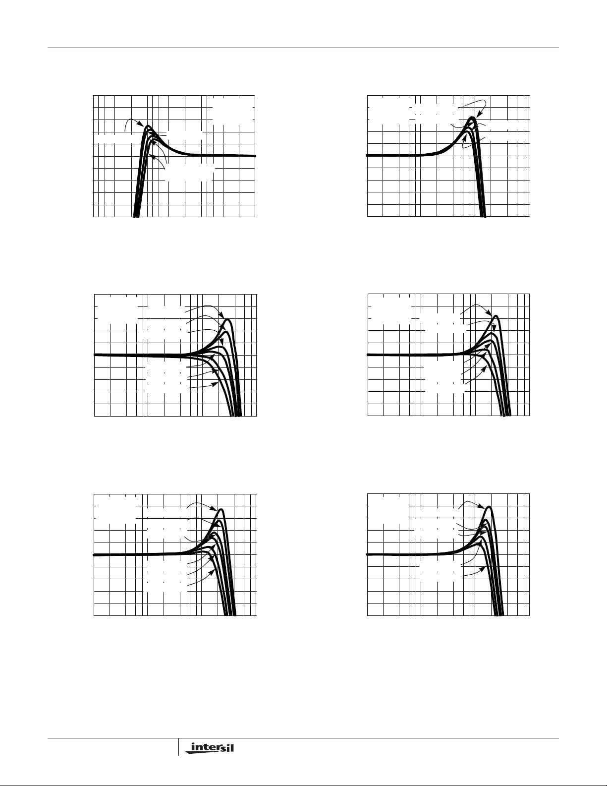
FIGURE 1. DRIVER DIFFERENTIAL FREQUENCY
RESPONSE vs R
25
VS=±12V
A
=10
V
=100Ω
R
L
20
GAIN (dB)
15
100K
(FULL POWER MODE)
F
RF=1.5kΩ
RF=1.82kΩ
RF=2.0kΩ
RF=2.43kΩ
RF=2.74kΩ
1M 100M
FREQUENCY (Hz)
RF=1.3kΩ
10M
FIGURE 3. DRIVER DIFFERENTIAL FREQUENCY
RESPONSE vs R
(2/3 POWER MODE)
F
FIGURE 2. DRIVER DIFFERENTIAL FREQUENCY
RESPONSE vs RF (FULL POWER MODE)
25
VS=±5V
A
=10
V
=100Ω
R
L
20
GAIN (dB)
15
100K
RF=1.3kΩ
RF=1.5kΩ
RF=2.0kΩ
RF=2.4kΩ
RF=2.74kΩ
1M 100M
FREQUENCY (Hz)
RF=1.82kΩ
10M
FIGURE 4. DRIVER DIFFERENTIAL FREQUENCY
RESPONSE vs RF (2/3 POWER MODE)
4
FN7039.2
March 26, 2007
Page 5
www.BDTIC.com/Intersil
Typical Performance Curves (Continued)
EL1503A
GAIN (dB)
25
20
15
RF=1.82kΩ
RF=2.0kΩ
RF=2.43kΩ
RF=2.74kΩ
10M
FREQUENCY (Hz)
1M100M
VS=±12V
=10
A
V
=100Ω
R
L
FIGURE 5. DRIVER DIFFERENTIAL FREQUENCY
RESPONSE vs R
19
VS=±12V
=5
A
V
R
=100Ω
L
14
GAIN (dB)
(TERMINATE MODE)
F
RF=1.3kΩ
RF=1.5kΩ
RF=1.82kΩ
RF=2.0kΩ
RF=2.4kΩ
RF=2.74kΩ
100K
25
VS=±5V
=10
A
V
=100Ω
R
L
20
GAIN (dB)
15
100K
RF=1.84kΩ
RF=2.0kΩ
1M 100M
FREQUENCY (Hz)
RF=2.43kΩ
RF=2.74kΩ
10M
FIGURE 6. DRIVER DIFFERENTIAL FREQUENCY
RESPONSE vs RF (TERMINATE MODE)
19
VS=±5V
=5
A
V
R
=100Ω
L
14
GAIN (dB)
RF=1.5kΩ
RF=1.82kΩ
RF=2.0kΩ
RF=2.4k
RF=2.74k
9
100K
1M 100M
FREQUENCY (Hz)
10M
FIGURE 7. DRIVER DIFFERENTIAL FREQUENCY
RESPONSE vs R
19
VS=±12V
A
=5
V
=100Ω
R
L
14
GAIN (dB)
9
100K
(FULL POWER MODE)
F
RF=1.3kΩ
RF=1.5kΩ
RF=1.82kΩ
RF=2.0kΩ
RF=2.43kΩ
RF=2.74kΩ
1M 100M
FREQUENCY (Hz)
10M
FIGURE 9. DRIVER DIFFERENTIAL FREQUENCY
RESPONSE vs R
(2/3 POWER MODE)
F
9
100K
1M 100M
FREQUENCY (Hz)
10M
FIGURE 8. DRIVER DIFFERENTIAL FREQUENCY
RESPONSE vs RF (FULL POWER MODE)
19
VS=±5V
A
=5
V
=100Ω
R
L
14
GAIN (dB)
9
100K
RF=1.5kΩ
RF=1.82kΩ
RF=2.0kΩ
RF=2.4kΩ
RF=2.74kΩ
1M 100M
FREQUENCY (Hz)
10M
FIGURE 10. DRIVER DIFFERENTIAL FREQUENCY
RESPONSE vs RF (2/3 POWER MODE)
5
FN7039.2
March 26, 2007
Page 6
www.BDTIC.com/Intersil
Typical Performance Curves (Continued)
EL1503A
19
RF=1.82kΩ
RF=2.0kΩ
RF=2.43kΩ
14
GAIN (dB)
VS=±12V
A
V
R
L
9
100K
=5
=100Ω
RF=2.74kΩ
1M 100M
FREQUENCY (Hz)
10M
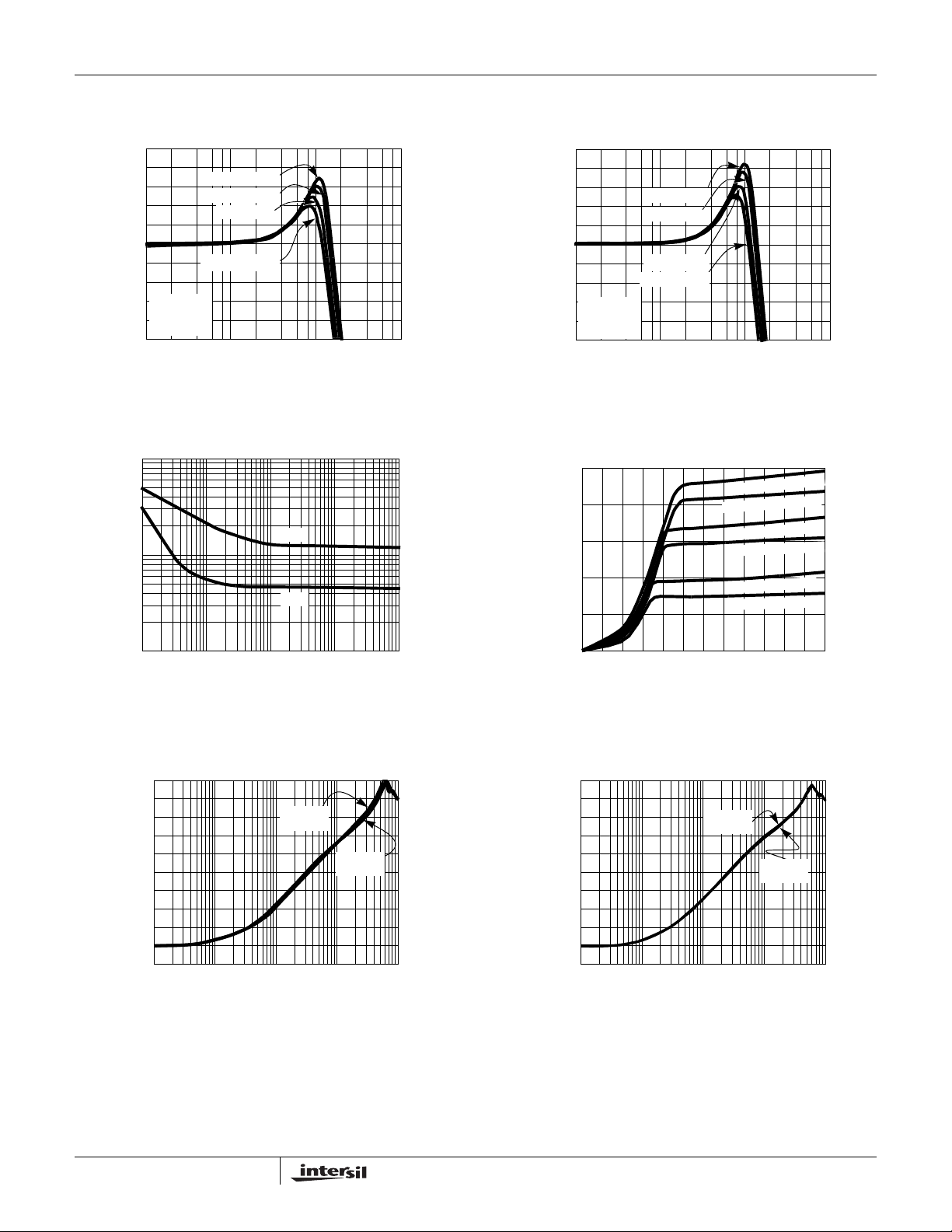
FIGURE 11. DRIVER DIF FERENTIAL FREQUENCY
(TERMINATE MODE)
F
i
N
e
N
(nV/√Hz)
N
e
RESPONSE vs R
100
10
100
10
(pA/√Hz)
N
i
19
RF=1.82kΩ
R
=2.0kΩ
F
14
GAIN (dB)
VS=±5V
A
=5
V
=100Ω
R
L
9
100K
RF=2.4kΩ
RF=2.74kΩ
1M 100M
FREQUENCY (Hz)
10M
FIGURE 12. DRIVER DIFFERENTIAL FREQUENCY
RESPONSE vs RF (TERMINATE MODE)
(mA)
S
I
25
(F
+
I
S
FU
(
20
15
10
5
-
I
S
+
I
S
-
I
S
(
-
I
S
W
PO
L
L
U
W
O
P
LL
E
W
O
P
3
/
2
(
WE
O
P
3
/
2
(
+
I
S
A
MIN
R
E
T
)
ER
)
R
E
)
R
)
R
)
E
T
1
10
100 100K1K
FREQUENCY (Hz)
10K
FIGURE 13. DRIVER INPUT VOLT AGE and FEEDBACK
1
0
2610
41208
VS (V)
FIGURE 14. SUPPLY CURRENT vs SUPPLY VOLTAGE
CURRENT NOISE vs FREQUENCY
0
-20
-40
-60
-80
SUPPLY REJECTION (dB)
-100
10K 100K 100M1M
LEFT
DRIVER
FREQUENCY (Hz)
DRIVER
10M
RIGHT
0
-20
-40
-60
-80
SUPPLY REJECTION (dB)
-100
10K 100K 100M1M
LEFT
DRIVER
FREQUENCY (Hz)
RIGHT
DRIVER
10M
FIGURE 15. POSITIVE SUPPLY REJECTION vs FREQUENCY FIGURE 16. NEGATIVE SUPPLY REJECTION vs FREQUENCY
6
FN7039.2
March 26, 2007
Page 7

www.BDTIC.com/Intersil
Typical Performance Curves (Continued)
EL1503A
100
VS=±12V
=1
A
V
=1.5kΩ
R
L
10
1
OUTPUT IMPEDANCE (Ω)
0
100K 10M
TERMINATE
2/3 POWER
FULL POWER
100M10K 1M
FREQUENCY (Hz)
100
VS=±5V
=1
A
V
=1.5kΩ
R
L
10
1
OUTPUT IMPEDANCE (Ω)
0
100K 10M
TERMINATE
2/3 POWER
FULL POWER
FREQUENCY (Hz)
FIGURE 17. OUTPUT IMPEDANCE vs FREQUENCY FIGURE 18. OUTPUT IMPEDANCE vs FREQUENCY
-45
VS=±12V
=5
A
V
R
=100Ω
L
-55
=1MHz
f
C
-65
HD (dB)
-75
-85
1 5 9 131721
V
OP-P
HD3
HD2
(V)
FIGURE 19. DIFFERENTIAL HARMONIC DIST ORTION vs
OUTPUT AMPLITUDE (FULL POWER)
-40
VS=±5V
-45
=5
A
V
=100Ω
R
L
-50
f
=1MHz
C
-55
-60
-65
HD (dB)
-70
-75
-80
-85
123 5 78
HD3
HD2
46
V
(V)
OP-P
FIGURE 20. DIFFERENTIAL HARMONIC DIST ORTION vs
OUTPUT AMPLITUDE (FULL POWER)
100M10K 1M
-50
VS=±5V
A
=5
V
-55
=100Ω
R
L
f
=1MHz
C
-60
-65
-70
HD (dB)
-75
-80
-85
1 5 9 131721
HD3
HD2
V
OP-P
(V)
FIGURE 21. DIFFERENTIAL HARMONIC DIST ORTION vs
OUTPUT AMPLITUDE (2/3 POWER)
7
-40
VS=±5V
=5
A
V
=100Ω
R
L
-50
f
=1MHz
C
-60
HD (dB)
-70
-80
123 5 78
HD3
HD2
46
V
(V)
OP-P
FIGURE 22. DIFFERENTIAL HARMONIC DIST ORTION vs
OUTPUT AMPLITUDE
March 26, 2007
FN7039.2
Page 8

www.BDTIC.com/Intersil
Typical Performance Curves (Continued)
EL1503A
-45
VS=±12V
=5
A
-50
V
=100Ω
R
L
f
=1MHz
C
-55
-60
-65
THD (dB)
-70
-75
-80
1 5 9 131721
2/3 POWER
FULL POWER
V
(V)
OP-P
FIGURE 23. DIFFERENTIAL TOTAL HARMONIC DISTORTION
vs OUTPUT AMPLITUDE
-60
-62
-64
-66
-68
-70
HD (dB)
-72
-74
-76
-78
3711 17
HD2
VS=±12V
=5
A
HD3
515
V
9
OP-P
(V)
V
R
L
f
C
=100Ω
=1MHz
19113
-40
VS=±5V
A
=5
V
=100Ω
R
L
=1MHz
f
-50
C
-60
THD (dB)
-70
-80
FULL POWER
2/3 POWER
123 5 78
46
V
(V)
OP-P
FIGURE 24. DIFFERENTIAL TOTAL HARMONIC DISTORTION
vs OUTPUT AMPLITUDE
-56
-60
-64
-68
HD (dB)
-72
-76
-80
HD2
VS=±5V
=5
HD3
25
3
V
OP-P
(V)
A
V
R
=100Ω
L
=1MHz
f
C
614
FIGURE 25. DIFFERENTIAL HARMONIC DIST ORTION vs
OUTPUT AMPLITUDE (FULL POWER)
-54
VS=±12V
-56
=5
A
V
=100Ω
R
L
-58
f
=1MHz
C
-60
-62
HD (dB)
-64
-66
-68
-70
515
3711 17
V
9
OP-P
HD2
HD3
19113
(V)
FIGURE 27. DIFFERENTIAL HARMONIC DIST ORTION vs
OUTPUT AMPLITUDE (2/3 POWER)
FIGURE 26. DIFFERENTIAL HARMONIC DIST ORTION vs
OUTPUT AMPLITUDE (FULL POWER)
-58
VS=±5V
=5
A
-60
V
=100Ω
R
L
f
=1MHz
C
-62
-64
-66
HD (dB)
-68
-70
-72
25
HD2
HD3
3
V
OP-P
614
(V)
FIGURE 28. DIFFERENTIAL HARMONIC DIST ORTION vs
OUTPUT AMPLITUDE (2/3 POWER)
8
FN7039.2
March 26, 2007
Page 9

www.BDTIC.com/Intersil
Typical Performance Curves (Continued)
EL1503A
-55
VS=±12V
=5
A
V
-57
R
=100Ω
L
=1MHz
f
C
-59
-61
THD (dBc)
-63
-65
-67
31117
2/3 POWER
FULL POWER
719115
9513
V
(V)
OP-P
FIGURE 29. DIFFERENTIAL TOTAL HARMONIC DISTORTION
vs OUTPUT AMPLITUDE
35
E
OD
M
R
E
OW
P
L
L
U
2/
±VS (V)
F
E
D
O
M
R
E
W
O
P
3
E
D
O
M
E
T
A
N
I
M
R
E
T
30
25
20
BW (MHz)
15
10
5
AV=10
=1.82kΩ
R
F
6 7 8 9 10 11 12
-55
VS=±5V
=5
A
V
-57
R
=100Ω
L
=1MHz
f
C
-59
-61
THD (dBc)
-63
-65
-67
26
2/3 POWER
471
V
(V)
OP-P
FULL POWER
53
FIGURE 30. DIFFERENTIAL TOTAL HARMONIC DISTORTION
vs OUTPUT AMPLITUDE
3.5
3.0
2.5
2.0
1.5
PEAKING (dB)
1.0
0.5
0
5
T
E
F
U
6 7 8 9 101112
±VS (V)
AV=10
=1.82kΩ
R
F
R
M
I
N
A
T
E
M
O
D
E
2
/
3
P
O
W
E
R
M
O
D
E
L
L
POW
ER
M
O
D
E
FIGURE 31. DIFFERENTIAL BANDWIDTH vs SUPPLY
VOLTAGE
(mA)
S
±I
25
20
15
10
5
0
0
IS+ (FULL POWER)
IS- (FULL POWER)
IS+ 2/3 POWER)
IS- 2/3 POWER)
28
FIGURE 33. I
410
R
(kΩ)
SET
vs R
S
VS = ±12V
to GND
R
SET
IS+ (TERMINATE)
IS- (TERMINATE)
6
SET
FIGURE 32. DIFFERENTIAL PEAKING vs SUPPLY VOLTAGE
(mA)
S
±I
25
IS+ (FULL POWER)
20
15
10
5
0
0
IS- (FULL POWER)
IS+ 2/3 POWER)
IS- 2/3 POWER)
28
410
R
(kΩ)
SET
FIGURE 34. IS vs R
VS = ±5V
to GND
R
SET
IS+ (TERMINATE)
IS- (TERMINATE)
6
SET
9
FN7039.2
March 26, 2007
Page 10

www.BDTIC.com/Intersil
Typical Performance Curves (Continued)
EL1503A
25
VS = ±12V
(mA)
S
±I
20
15
10
5
0
100 5000 300
200 400
I
SET
I
S
(µA)
(
+
FIGURE 35. IS vs I
4.5
4.0
3.5
3.0
2.5
2.0
1.5
1.0
POWER DISSIPATION (W)
0.5
0
-40 20-20 60 80
θJA = 30°C/W
θJA = 43°C/W
θJA = 53°C/W
θJA = 80°C/W
0 100
AMBIENT TEMPERATURE (°C)
40
F
I
U
-
S
I
SET
E
W
O
P
L
O
L
P
L
L
U
F
(
3
/
2
(
+
I
S
3
/
2
(
-
I
S
RM
E
(T
+
S
R
E
T
(
-
I
S
FIGURE 37. POWER DISSIPA TION vs AMBIENT
TEMPERATURE for VARIOUS MOUNTED θ
)
R
)
R
E
W
R)
E
W
O
P
)
R
E
W
O
P
)
E
NAT
I
)
E
AT
N
I
M
s
JA
25
VS = ±12V
20
(mA)
S
±I
15
10
5
0
100 5000 300
200 400
I
SET
I
(µA)
FIGURE 36. IS vs I
POWER DISSIPATION & THERMAL RESISTANCE USING
JEDEC JESD51-7 HIGH EFFECTIVE THERMAL
CONDUCTIVITY (4-LA YER) TEST BOARD, QFN EXPOSED
DIEPAD SOLDERED TO PCB PER JESD51-5
3.0
2.5
2.703W
2.0
1.5
1.0
0.5
POWER DISSIPATION (W)
0
AMBIENT TEMPERATURE (°C)
Q
θ
F
J
N
A
2
=
4
3
7
°
C
/
W
85
I
S
-
S
SET
P
L
L
U
F
(
O
+
P
L
L
U
F
(
3
/
2
(
+
I
S
3
/
2
(
-
I
S
R
E
T
(
+
I
S
R
E
T
(
-
I
S
FIGURE 38. POWER DISSIPATION vs AMBIENT
)
R
E
W
O
)
R
E
W
)
R
E
W
O
P
)
R
E
W
O
P
)
E
T
A
N
I
M
)
E
T
A
N
I
M
1500 25 50 75 100 125
TEMPERATURE
10
FN7039.2
March 26, 2007
Page 11

www.BDTIC.com/Intersil
Test Circuit
V
1
IN
V
2
OUT
-A VIN-B
EL1503A
A
V
OUT
20
19
B
LEFT
DRIVER
OUT
GND
0.1µF 5µF
TANTALUM
R
56Ω
1/2W
-
V
3
S
GND
4
GND
5
GND
6
GND
7
VIN+A
8
C
9
1
C
10
0
3
R
1.5kΩ
C
2
7
1
2
3
4
5
332Ω
AB
-+
R
100
1W
S
V
GND
GND
GND
GND
V
IN
I
ADJ
NC
-+
S
+B
+
18
17
16
15
14
13
12
11
R
4
56Ω
1/2W
R
16
20
19
18
17
16
1.5kΩ
5µF 0.1µF
C
1
TANTALUM
RIGHT
DRIVER
OUT
+
V
S
GND
15
14
13
12
11
LEFT
DRIVER
6
7
IN
R
2
51Ω
C
C
1
0
8
9
10
11
RIGHT
DRIVER
R
17
51Ω
R
SET
IN
FN7039.2
March 26, 2007
Page 12

www.BDTIC.com/Intersil
EL1503A
Pin Descriptions
20 Ld SOIC
(0.300") 24 Ld QFN PIN NAME FUNCTION CIRCUIT
123V
224V
33V
4, 5, 6, 7 7 GND Ground Connection
88V
-A Channel A Inverting Input
IN
A Channel A Output (Reference Circuit 1)
OUT
- Negative Supply
S
+A Channel A Non-Inverting Input
IN
CIRCUIT 1
VS+
99C
10 10 C
11 1, 2, 4, 5, 6, 14,
12 11 I
13 12 V
14, 15, 16, 17 13 GND Ground Connection
18 17 V
19 20 V
20 21 V
- 7 Reserve for Future Use Internally Unconnected
15, 16, 18, 19,
22
1
0
NC Not Connected
ADJ
+B Channel B Non-Inverting Input (Reference Circuit 2)
IN
+ Positive Supply
S
OUT
-B Channel B Inverting Input (Reference Circuit 1)
IN
Current Control Bit 1
Current Control Bit 0 (Reference Circuit 3)
Supply Current Control Pin
B Channel B Output (Reference Circuit 1)
CIRCUIT 2
VS-
VS+
6.7V
CIRCUIT 3
VS+
CIRCUIT 4
12
FN7039.2
March 26, 2007
Page 13

www.BDTIC.com/Intersil
EL1503A
Applications Information
The EL1503A consists of two high-power line driver
amplifiers that can be connected for full duplex differential
line transmission. The amplifiers are designed to be used
with signals up to 4MHz and produce low distortion levels. A
typical interface circuit is shown in Figure 39 below.
R
DRIVER
INPUT
RECEIVE
OUT +
RECEIVE
OUT -
FIGURE 39. TYPICAL LINE INTERFACE CONNECTION
RECEIVE
AMPLIFIERS
+
-
R
F
R
G
R
F
-
+
R
R
F
R
IN
-
+
+
R
-
R
R
IN
F
OUT
R
OUT
LINE +
Z
LINE
LINE -
can cause ringing or even oscillations. This inductance is
equivalent to about 4” of unshielded wiring, or 6” of
unterminated transmission line. Normal high-frequency
construction obviates any such problem.
Power Supplies & Dissipation
Due to the high power drive capability of the EL1503A, much
attention needs to be paid to power dissipation. The power
that needs to be dissipated in the EL1503A has two main
contributors. The first is the quiescent current dissipation.
The second is the dissipation of the output stage.
The quiescent power in the EL1503A is not constant with
varying outputs. In reality, 7mA of the 12.5mA needed to
power each driver is converted in to output current.
Therefore, in the equation below we should subtract the
average output current, I
We’ll call this term I
Therefore, we can determine a quiescent current with the
equation:
P
DquiescentVSIS2IX
where:
VS is the supply voltage (VS+ to VS-)
, or 7mA, whichever is the lowest.
O
.
X
–()×=
The amplifiers are wired with one in positive gain and the
other in a negative gain configuration to generate a
differential output for a single-ended input. They will exhibit
very similar frequency responses for gains of three or
greater and thus generate very small common-mode outputs
over frequency, but for low gains the two drivers R
's need
F
to be adjusted to give similar frequency responses. The
positive-gain driver will generally exhibit more bandwidth and
peaking than the negative-gain driver.
If a differential signal is available to the drive amplifiers, they
may be wired so:
+
-
R
F
2R
G
R
F
-
+
FIGURE 40. DRIVERS WIRED FOR DIFFERENTIAL INPUT
Each amplifier has identical positive gain connections, and
optimum common-mode rejection occurs. Further, DC input
errors are duplicated and create common-mode rather than
differential line errors.
Input Connections
The EL1503A amplifiers are somewhat sensitive to source
impedance. In particular, they do not like being driven by
inductive sources. More than 100nH of source impedance
IS is the maximum quiescent supply current (IS+ + IS-)
IX is the lesser of IO or 7mA (generally IX = 7mA)
The dissipation in the output stage has two main
contributors. Firstly, we have the average voltage drop
across the output transistor and secondly, the average
output current. For minimal power dissipation, the user
should select the supply voltage and the line transformer
ratio accordingly. The supply voltage should be kept as low
as possible, while the transformer ratio should be selected
so that the peak voltage required from the EL1503A is close
to the maximum available output swing. There is a trade of
however with the selection of transformer ratio. As the ratio
is increased, the receive signal available to the receivers is
reduced.
Once the user has selected the transformer ratio, the
dissipation in the output stages can be selected with the
following equation:
P
Dtransistors
=
2I
O
⎛
-------
×× V
⎝
⎞
–
O
⎠
2
V
S
where:
V
is the supply voltage (VS+ to VS-)
S
VO is the average output voltage per channel
IO is the average output current per channel
The overall power dissipation (P
P
Dquiescent
and P
Dtransistor
.
) is obtained by adding
DISS
13
FN7039.2
March 26, 2007
Page 14

www.BDTIC.com/Intersil
EL1503A
Then, the θJA requirement needs to be calculated. This is
done using the equation:
T
-------------------------------------------------
θ
=
JA
–()
JUNCTTAMB
P
DISS
where:
T
T
P
θ
is the maximum die temperature (150°C)
JUNCT
is the maximum ambient temperature
AMB
is the dissipation calculated above
DISS
is the junction to ambient thermal resistance for the
JA
package when mounted on the PCB
This θJA value is then used to calculate the area of copper
needed on the board to dissipate the power. The graph
below show various
θ
for the SO20 mounted on different
JA
copper foil areas.
55
50
(°C/W)
JA
45
40
35
MOUNTED DEVICE θ
30
012 910678345
FIGURE 41. THERMAL RESISTANCE of 20 Ld SOIC (0.300")
TOP FOIL ONLY-NO SOLDER MASK
AREA OF CIRCUIT BOARD HEAT SINK (in
EL1503A vs BOARD COPPER AREA
Note: 2oz. COPPER USED
TOP FOIL ONLY-WITH SOLDER MASK
TOP FOIL-WITH 0.45IN2 BOTTOM
FOIL WITH MANY FEEDTHROUGHS
2
)
A separate application note details the 24 Ld QFN PCB
design considerations.
Single Supply Operation
The EL1503A can also be powered from a single supply
voltage. When operating in this mode, the GND pins can still
be connected directly to GND. To calculate power
dissipation, the equations in the previous section should be
used, with V
equal to half the supply rail.
S
EL1503A PCB Design
A separate application note details the 24 Ld QFN PCB
design considerations. The SOIC power packages
(20 leads) are designed so that heat may be conducted
away from the device in an efficient manner. To disperse this
heat, the center leads (4 per side for the 20 lead and 2 per
side for the 16 lead) are internally connected to the mounting
platform of the die. Heat flows through the leads into the
circuit board copper, then spreads and convects to air . Thus,
the ground plane on the component side of the board
becomes the heatsink. This has proven to be a very effective
technique, but several aspects of board layout should be
noted. First, the heat should not be shunted to internal
copper layers of the board nor backside foil, since the
feedthroughs and fiberglass of the board are not very
thermally conductive. To obtain the best thermal resistance
of the mounted part,
θ
, the topside copper ground plane
JA
should have as much area as possible and be as thick as
practical. If possible, the solder mask should be cut away
from the EL1503A to improve thermal resistance. Finally,
metal heatsinks can be placed against the board close to the
part to draw heat toward the chassis.
Output Loading
While the drive amplifiers can output in excess of 500mA
transiently, the internal metallization is not designed to carry
more than 100mA of steady DC current and there is no
current-limit mechanism. This allows safely driving rms
sinusoidal currents of 2 X 100mA, or 200mA. This current is
more than that required to drive line impedances to large
output levels, but output short circuits cannot be tolerated.
The series output resistor will usually limit currents to safe
values in the event of line shorts. Driving lines with no series
resistor is a serious hazard.
The amplifiers are sensitive to capacitive loading. More than
25pF will cause peaking of the frequency response. The
same is true of badly terminated lines connected without a
series matching resistor.
Power Supplies
The power supplies should be well bypassed close to the
EL1503A. A 3.3µF tantalum capacitor for each supply works
well. Since the load currents are differential, they should not
travel through the board copper and set up ground loops that
can return to amplifier inputs. Due to the class AB output
stage design, these currents have heavy harmonic content.
If the ground terminal of the positive and negative bypass
capacitors are connected to each other directly and then
returned to circuit ground, no such ground loops will occur.
This scheme is employed in the layout of the EL1503A
demonstration board, and documentation can be obtained
from the factory.
Feedback Resistor Value
The bandwidth and peaking of the amplifiers varies with
supply voltage somewhat and with gain settings. The
feedback resistor values can be adjusted to produce an
optimal frequency response. Here is a series of resistor
values that produce an optimal driver frequency response
(1dB peaking) for different supply voltages and gains:
TABLE 1. OPTIMUM DRIVER FEEDBACK RESISTOR for
VARIOUS GAINS and SUPPLY VOLTAGES
SUPPLY
VOLTAGE
±5V
±12V
DRIVER VOLTAGE GAIN
2.5 5 10
2.7k
2.2k
2.2k
2.0k
2.0k
2.0k
14
FN7039.2
March 26, 2007
Page 15

www.BDTIC.com/Intersil
EL1503A
Power Control Function
The EL1503A contains two forms of power control operation.
Two digital inputs, C
supply current of the EL1503A drive amplifiers. As the
supply current is reduced, the EL1503A will start to exhibit
slightly higher levels of distortion and the frequency
response will be limited. The 4 power modes of the EL1503A
are set up as shown in the table 2.
TABLE 2. POWER MODES of the EL1503A
C
1
00I
012/3 I
101/3 I
1 1 Power down
and C1, can be used to control the
0
C
0
full power mode (CO or CP)
S
power mode (CO or CP)
S
terminate only mode
S
OPERATION
Another method for controlling the power consumption of the
EL1503A is to connect a resistor from the I
pin to ground.
ADJ
When this pin is grounded (the normal state), the supply
current per channel is as per the specifications table on page
3. When a resistor is inserted, the supply current is scaled
according to the “I
vs R
S
” graphs on page 10 in the
SET
Performance Curves section.
Both methods of power control can be used simultaneously.
In this case, positive and negative supply currents (per amp)
are given by the equations below:
12.5mA
+
=
IS+1mAC(123)⁄
-------------------------------------------
13)⁄
+
C(
0
IS-0C(123)⁄
( 13)⁄
C
0
××
++=
1( R
-------------------------------------------
××
1( R
-------------------------------------------
××
1( R
12.5mA
12.5mA
1k)÷+
SET
12.5mA
-------------------------------------------
××
1( R
1k)÷+
SET
SET
SET
1k)÷+
1k)÷+
All Intersil U.S. products are manufactured, assembled and tested utilizing ISO9000 quality systems.
Intersil Corporation’s quality certifications can be viewed at www.intersil.com/design/quality
Intersil products are sold by description only. Intersil Corporation reserves the right to make changes in circuit design, software and/or specifications at any time without
notice. Accordingly, the reader is cautioned to verify that data sheets are current before placing orders. Information furnished by Intersil is believed to be accurate and
reliable. However, no responsibility is assumed by Intersil or its subsidiaries for its use; nor for any infringements of patents or other rights of third parties which may result
from its use. No license is granted by implic atio n or other wise u nde r any p a tent or patent rights of Intersil or its subsidi aries.
For information regarding Intersil Corporation and its products, see www.intersil.com
15
FN7039.2
March 26, 2007
Page 16
www.BDTIC.com/Intersil
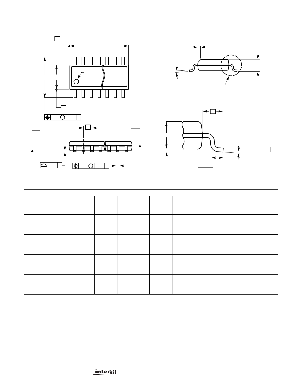
Small Outline Package Family (SO)
A
D
NN
(N/2)+1
EL1503A
h X 45°
PIN #1
E
C
SEATING
PLANE
0.004 C
E1
B
0.010 BM CA
I.D. MARK
1
e
0.010 BM CA
(N/2)
c
SEE DETAIL “X”
L1
H
A2
GAUGE
PLANE
A1
b
DETAIL X
L
4° ±4°
MDP0027
SMALL OUTLINE PACKAGE FAMILY (SO)
INCHES
SO16
SYMBOL
A 0.068 0.068 0.068 0.104 0.104 0.104 0.104 MAX -
A1 0.006 0.006 0.006 0.007 0.007 0.007 0.007 ±0.003 A2 0.057 0.057 0.057 0.092 0.092 0.092 0.092 ±0.002 -
b 0.017 0.017 0.017 0.017 0.017 0.017 0.017 ±0.003 -
c 0.009 0.009 0.009 0.011 0.011 0.011 0.011 ±0.001 D 0.193 0.341 0.390 0.406 0.504 0.606 0.704 ±0.004 1, 3
E 0.236 0.236 0.236 0.406 0.406 0.406 0.406 ±0.008 -
E1 0.154 0.154 0.154 0.295 0.295 0.295 0.295 ±0.004 2, 3
e 0.050 0.050 0.050 0.050 0.050 0.050 0.050 Basic -
L 0.025 0.025 0.025 0.030 0.030 0.030 0.030 ±0.009 -
L1 0.041 0.041 0.041 0.056 0.056 0.056 0.056 Basic -
h 0.013 0.013 0.013 0.020 0.020 0.020 0.020 Reference -
N 8 14 16 16 20 24 28 Reference -
NOTES:
1. Plastic or metal protrusions of 0.006” maximum per side are not included.
2. Plastic interlead protrusions of 0.010” maximum per side are not included.
3. Dimensions “D” and “E1” are measured at Datum Plane “H”.
4. Dimensioning and tolerancing per ASME Y14.5M-1994
(0.150”)
SO16 (0.300”)
(SOL-16)
SO20
(SOL-20)
SO24
(SOL-24)
SO28
(SOL-28)
TOLERANCE NOTESSO-8 SO-14
A
0.010
Rev. M 2/07
16
FN7039.2
March 26, 2007
Page 17

www.BDTIC.com/Intersil
EL1503A
QFN (Quad Flat No-Lead) Package Family
A
1
2
3
2X
0.075 C
L
(E2)
C
SEATING
PLANE
0.08 C
N LEADS
& EXPOSED PAD
A
C
N
(N-2)
(N-1)
PIN #1
I.D. MARK
TOP VIEW
0.10 BAMC
b
N LEADS
(N/2)
(D2)
BOTTOM VIEW
e
SIDE VIEW
(c)
A1
DETAIL X
D
(N/2)
(N-2)
(N-1)
N
0.10
SEE DETAIL "X"
2
(L)
N LEADS
0.075
PIN #1 I.D.
1
2
3
NE
7
C
2X
B
E
C
3
5
MDP0046
QFN (QUAD FLAT NO-LEAD) PACKAGE FAMILY
(COMPLIANT TO JEDEC MO-220)
MILLIMETERS
SYMBOL
A 0.90 0.90 0.90 0.90 ±0.10 -
A1 0.02 0.02 0.02 0.02 +0.03/-0.02 -
b 0.25 0.25 0.23 0.22 ±0.02 c 0.20 0.20 0.20 0.20 Reference D 7.00 5.00 8.00 5.00 Basic -
D2 5.10 3.80 5.80 3.60/2.48 Reference 8
E 7.00 7.00 8.00 6.00 Basic -
E2 5.10 5.80 5.80 4.60/3.40 Reference 8
e 0.50 0.50 0.80 0.50 Basic L 0.55 0.40 0.53 0.50 ±0.05 -
N 44 38 32 32 Reference 4
ND 11 7 8 7 Reference 6
NE 11 12 8 9 Reference 5
MILLIMETERS
SYMBOL
A 0.90 0.90 0.90 0.90 0.90 ±0.10 -
A1 0.02 0.02 0.02 0.02 0.02 +0.03/
b 0.25 0.25 0.30 0.25 0.33 ±0.02 -
c 0.20 0.20 0.20 0.20 0.20 Reference -
D 4.00 4.00 5.00 4.00 4.00 Basic D2 2.65 2.80 3.70 2.70 2.40 Reference -
E 5.00 5.00 5.00 4.00 4.00 Basic -
E2 3.65 3.80 3.70 2.70 2.40 Reference -
e 0.50 0.50 0.65 0.50 0.65 Basic -
L 0.40 0.40 0.40 0.40 0.60 ±0.05 -
N 28 24 20 20 16 Reference 4
ND 6 5 5 5 4 Reference 6
NE 8 7 5 5 4 Reference 5
NOTES:
1. Dimensioning and tolerancing per ASME Y14.5M-1994.
2. Tiebar view shown is a non-functional feature.
3. Bottom-side pin #1 I.D. is a diepad chamfer as shown.
4. N is the total number of terminals on the device.
5. NE is the number of terminals on the “E” side of the package
(or Y-direction).
6. ND is the number of terminals on the “D” side of the package
(or X-direction). ND = (N/2)-NE.
7. Inward end of terminal may be square or circular in shape with radius
(b/2) as shown.
8. If two values are listed, multiple exposed pad options are available.
Refer to device-specific datasheet.
TOLERANCE NOTESQFN44 QFN3 QFN32
TOLER-
ANCE NOTESQFN28 QFN2 QFN20 QFN16
-0.02
Rev 11 2/07
-
17
FN7039.2
March 26, 2007
 Loading...