

查询DG507A供应商
DG506A, DG507A, DG508A, DG509A
Data Sheet November 1999
CMOS Analog Multiplexers
The DG506A, DG507A, DG508A and DG509A are CMOS
Monolithic 16-Channel/Dual 8-Channel and 8-Channel/Dual
4-Channel Analog Multiplexers, which can also be used as
demultiplexers. An enable input is provided. When the
enable input is high, a channel is selected by the address
inputs, and when low, all channels are off.
A channel in the ON state conducts current equally well in
both directions. In the OFF state each channel blocks
voltages up to the supply rails. The address inputs and the
enable input are TTL and CMOS compatible over the full
specified operating temperature range.
The DG506A, DG507A, DG508A and DG509A are pinout
compatible with the industry standard devices.
Ordering Information
TEMP.
PART NUMBER
RANGE (oC) PACKAGE
DG506AAK -55 to 125 28 Ld CERDIP F28.6
DG506ACJ 0 to 70 28 Ld PDIP E28.6
DG506ACY 0 to 70 28 Ld SOIC M28.3
DG507ABK -25 to 85 28 Ld CERDIP F28.6
DG507ACJ 0 to 70 28 Ld PDIP E28.6
DG507ACY 0 to 70 28 Ld SOIC M28.3
PKG.
NO.
File Number 3137.3
Features
• Low Power Consumption
• TTL and CMOS-Compatible Address and Enable Inputs
• 44V Maximum Power Supply Rating
• High Latch-Up Immunity
• Break-Before-Make Switching
• Alternate Source
Applications
• Data Acquisition Systems
• Communication Systems
• Signal Multiplexing/Demultiplexing
• Audio Signal Multiplexing
TEMP.
PART NUMBER
RANGE (oC) PACKAGE
DG508AAK -55 to 125 16 Ld CERDIP F16.3
DG508ABK -25 to 85 16 Ld CERDIP F16.3
DG508ACJ 0 to 70 16 Ld PDIP E16.3
DG509ACJ 0 to 70 16 Ld PDIP E16.3
DG509ACY 0 to 70 16 Ld SOIC M16.3
PKG.
NO.
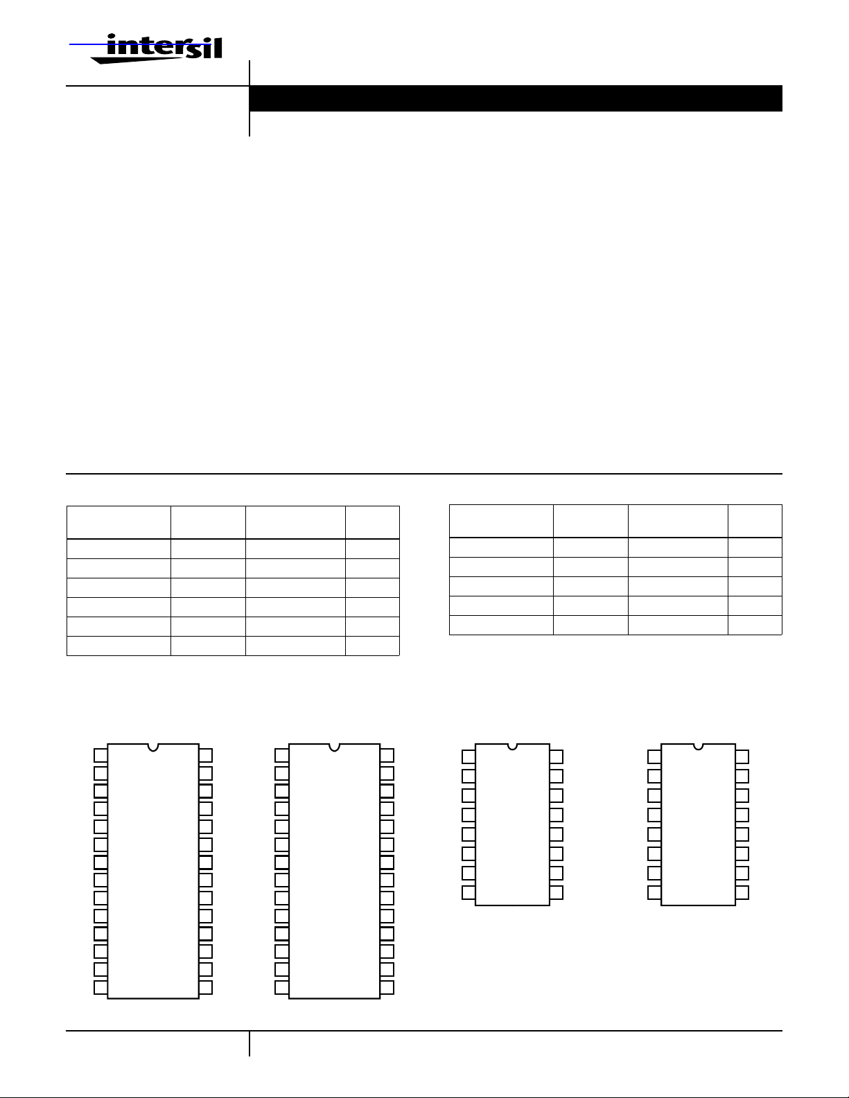
Pinouts
DG506A (PDIP, CERDIP, SOIC)
TOP VIEW
V+
NC
NC
S
S
S
S
S
S
S
S
GND
NC
A
1
2
3
4
16
5
15
6
14
7
13
8
12
9
11
10
10
11
9
12
13
14
3
28
27
26
25
24
23
22
21
20
19
18
17
16
15
DG507A (PDIP, CERDIP, SOIC)
TOP VIEW
D
VS
S
S
S
S
S
S
S
EN
A
A
A
V+
1
D
2
B
NC
S
8B
S
7B
S
6B
S
5B
S
4B
S
3B
S
2B
S
1B
GND
NC
NC
3
4
5
6
7
8
9
10
11
12
13
14
8
7
6
5
4
3
2
1
0
1
2
1
DG508A (PDIP, CERDIP)
TOP VIEW
D
28
A
V-
27
S
26
8A
S
25
7A
S
24
6A
S
23
5A
S
22
4A
21
S
3A
20
S
2A
19
S
1A
18
EN
A
17
0
A
16
1
A
15
2
CAUTION: These devices are sensitive to electrostatic discharge; follow proper IC Handling Procedures.
1
A
0
2
EN
V-
3
S
4
1
S
5
2
S
6
3
S
7
4
D
8
1-888-INTERSIL or 321-724-7143 | Copyright © Intersil Corporation 1999
16
A
1
A
15
2
14
GND
V+
13
S
12
5
S
11
6
S
10
7
S
9
8
DG509A (PDIP, SOIC)
TOP VIEW
A
1
0
2
EN
V-
3
S
4
1A
S
5
2A
S
6
3A
S
7
4A
D
8
A
A
16
1
GND
15
V+
14
S
13
1B
S
12
2B
S
11
3B
S
10
4B
D
9
B
Truth Tables
DG506A, DG507A, DG508A, DG509A
DG506A
A
3
A
2
A
1
A
EN ON SWITCH
0
XXXX0 None
00001 1
00011 2
00101 3
00111 4
01001 5
01011 6
01101 7
01111 8
10001 9
10011 10
10101 11
10111 12
11001 13
11011 14
11101 15
11111 16
Logic “0” = VAL,V
≤ 0.8V, Logic “1” = VAH,V
ENL
ENH
≥ 2.4V.
DG508A
A
2
A
1
A
0
EN ON SWITCH
X X X 0 None
0001 1
0011 2
0101 3
0111 4
1001 5
1011 6
1101 7
1111 8
A0, A1, A2, EN
Logic “1” = VAH≥ 2.4V, Logic “0” = VAL≤ 0.8V
DG507A
A
2
A
1
A
0
EN ON SWITCH
X X X 0 None
0001 1
0011 2
0101 3
0111 4
1001 5
1011 6
1101 7
1111 8
Logic “0” = VAL, V
≤ 0.8V, Logic “1” = VAH, V
ENL
ENH
≥ 2.4V.
DG509A
A
1
A
0
EN ON SWITCH
X X 0 None
0 0 1 1A, 1B
0 1 1 2A, 2B
1 0 1 3A, 3B
1 1 1 4A, 4B
A0, A1, EN
Logic “1” = VAH≥ 2.4V, Logic “0” = VAL≤ 0.8V.
2
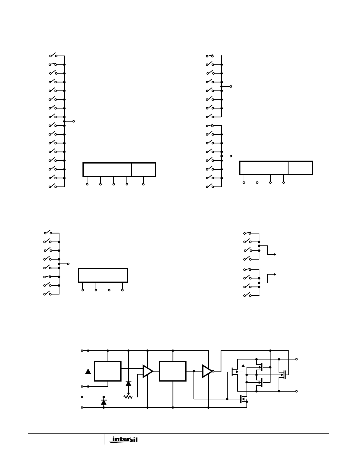
Functional Diagrams
DG506A
S
1
S
2
S
3
S
4
S
5
S
6
S
7
S
8
S
9
S
10
S
11
S
12
S
13
S
14
S
15
S
16
D
ADDRESS DECODER
A
0
DG506A, DG507A, DG508A, DG509A
1 OF 16
A1A2A
3
ENABLE
1 OF 4
EN
DG507A
S
1A
S
2A
S
3A
S
4A
S
5A
S
6A
S
7A
S
8A
S
1B
S
2B
S
3B
S
4B
S
5B
S
6B
S
7B
S
8B
D
A
D
B
ADDRESS DECODER
1 OF 8
A
A1A2EN (ENABLE INPUT)
0
ENABLE
1 OF 2
4 Line Binary Address Inputs
(0 0 0 1) and EN = 5V
Above example shows channel 2 turned ON.
DG508A
S
1
S
2
S
3
S
4
S
5
S
6
S
7
S
8
D
ADDRESS DECODER
1 OF 8
A
A1A2EN (ENABLE INPUT)
0
3 Line Binary Address Inputs
(1 0 1) and EN = 1
Above example shows channel 6 turned ON.
Schematic Diagram
V+
LOGIC TRIP
POINT REF
3 Line Binary Address Inputs
(0 0 0) and EN = 5V
Above example shows channels 1A and 1B turned ON.
DG509A
S
1A
S
2A
S
3A
S
4A
S
1B
S
2B
S
3B
S
4B
D
A
D
B
2 Line Binary Address Inputs
(0 0) and EN = 1
Above example shows channels 1A and 1B turned ON.
S
+
-
DECODER
A
X
V+
X
GND
LOGIC A
INPUT OR EN
X
V-
LOGIC INTERFACE
AND LEVEL SHIFTER
3
TYPICAL
SWITCH
D
X
DG506A, DG507A, DG508A, DG509A
Absolute Maximum Ratings Thermal Information
V+ to V- . . . . . . . . . . . . . . . . . . . . . . . . . . . . . . . . . . . . . . . . . . . 44V
V- to Ground. . . . . . . . . . . . . . . . . . . . . . . . . . . . . . . . . . . . . . . . 25V
Digital Inputs, VS, VD (Note 1). . . . . . . . . . . . . .(V- -2V) To (V+ +2V)
Continuous Current, (Any Terminal Except S or D). . . . . . . . . 30mA
Continuous Current, (S or D). . . . . . . . . . . . . . . . . . . . . . . . . . 20mA
Peak Current, S or D (Pulsed 1ms, 10% Duty Cycle Max) . . . . . 40mA
Operating Conditions
Temperature Range
“A” Suffix. . . . . . . . . . . . . . . . . . . . . . . . . . . . . . . . -55oC to 125oC
“B” Suffix. . . . . . . . . . . . . . . . . . . . . . . . . . . . . . . . . -25oC to 85oC
“C” Suffix . . . . . . . . . . . . . . . . . . . . . . . . . . . . . . . . . 0oC to 70oC
CAUTION: Stresses above those listed in “Absolute Maximum Ratings” may cause permanent damage to the device. This is a stress only rating and operation of the
device at these or any other conditions above those indicated in the operational sections of this specification is not implied.
NOTES:
1. Signals on SX, DX, EN, or AXexceeding V+ or V- are clamped by internal diodes. Limit diode current to maximum current ratings.
2. θJA is measured with the component mounted on an evaluation PC board in free air.
Thermal Resistance (Typical, Note 2) θJA (oC/W) θJC (oC/W)
16 Ld CERDIP Package. . . . . . . . . . . . 75 20
28 Ld CERDIP Package. . . . . . . . . . . . 55 18
16 Ld PDIP Package . . . . . . . . . . . . . . 90 N/A
28 Ld PDIP Package . . . . . . . . . . . . . . 55 N/A
16 Ld SOIC Package . . . . . . . . . . . . . . 100 N/A
28 Ld SOIC Package . . . . . . . . . . . . . . 70 N/A
Maximum Junction Temperature
CERDIP Package. . . . . . . . . . . . . . . . . . . . . . . . . . . . . . . . .175oC
PDIP Package . . . . . . . . . . . . . . . . . . . . . . . . . . . . . . . . . . .150oC
Maximum Storage Temperature
“A” and “B” Suffix . . . . . . . . . . . . . . . . . . . . . . . . . -65oC to 150oC
“C” Suffix . . . . . . . . . . . . . . . . . . . . . . . . . . . . . . . -65oC to 125oC
Maximum Lead Temperature (Soldering 10s) . . . . . . . . . . . . .300oC
(SOIC - Lead Tips Only)
Electrical Specifications T
= 25oC, V+ = +15V, V- = -15V, GND = 0V, VEN = 2.4V, Unless Otherwise Specified
A
“A” SUFFIX “B” AND “C” SUFFIX
(NOTE4)
PARAMETER TEST CONDITIONS
MIN
(NOTE3)
TYP
(NOTE4)
MAX
(NOTE4)
MIN
(NOTE3)
TYP
(NOTE4)
MAX
DYNAMIC CHARACTERISTICS
Switching Time of
Multiplexer, t
TRANSITION
Break-Before-Make
Interval, t
OPEN
Enable Turn-ON Time,
t
ON(EN)
Enable Turn-OFF Time,
t
OFF(EN)
OFF Isolation, OIRR V
Source OFF Capacitance,
C
S(OFF)
See Figure 1 - 0.6 1 - 0.6 - µs
See Figure 3 - 0.2 - - 0.2 - µs
See Figure 2 - 1 1.5 - 1 - µs
See Figure 2 - 0.4 1.0 - 0.4 - µs
= 0V, RL = 1kΩ, CL = 15pF,
EN
VS = 7V
, f = 500kHz (Note 5)
RMS
-68- -68-dB
VS = 0V, VEN = 0V, f = 140kHz
DG506A, DG507A - 6 - - 6 - pF
DG508A, DG509A - 5 - - 5 - pF
Drain OFF Capacitance,
C
D(OFF)
VD = 0V, VEN = 0V, f = 140kHz
DG506A - 45 - - 45 - pF
DG507A - 23 - - 23 - pF
DG508A - 25 - - 25 - pF
DG509A - 12 - - 12 - pF
Charge Injection, Q See Figure 4
DG506A, DG507A - 6 - - 6 - pC
DG508A, DG509A - 4 - - 4 - pC
DIGITAL INPUT CHARACTERISTICS
Address Input Current,
Input Voltage High, I
Address Input Current
Input Voltage Low, I
AL
VA = 2.4V -10 -0.002 - -10 -0.002 - µA
AH
= 15V - 0.006 10 - 0.006 10 µA
V
A
VEN = 2.4V VA = 0V -10 -0.002 - -10 -0.002 - µA
= 0V -10 -0.002 - -10 -0.0002 - µA
V
EN
UNITS
4
DG506A, DG507A, DG508A, DG509A
Electrical Specifications T
= 25oC, V+ = +15V, V- = -15V, GND = 0V, VEN = 2.4V, Unless Otherwise Specified (Continued)
A
“A” SUFFIX “B” AND “C” SUFFIX
(NOTE4)
PARAMETER TEST CONDITIONS
MIN
(NOTE3)
TYP
(NOTE4)
MAX
(NOTE4)
MIN
(NOTE3)
TYP
(NOTE4)
MAX
ANALOG SWITCH CHARACTERISTICS
Analog Signal Range,
V
ANALOG
Drain-Source ON
Resistance, r
DS(ON)
(Note 7) -15 - +15 -15 - +15 V
SequenceEach
Switch ON
VAL = 0.8V
IS = -200µA, VD = +10V - 270 400 - 270 450 Ω
= -200µA, VD = -10V - 230 400 - 230 450 Ω
I
S
VAH = 2.4V
r
Matching
DS(ON)
Between Channels
Source OFF Leakage
Current, I
S(OFF)
Drain OFF Leakage
Current, I
D(OFF)
-10V ≤ VS≤ +10V - 6 - - 6 - %
∆r
DS ON()
r
DS(ON)MAXrDS ON()MIN
----------------------------------------------------------------------- -=
–
r
DS ON()AVG
VEN = 0V VS = +10V, VD = -10V -1 0.002 1 -5 0.002 5 nA
= -10V, VD = +10V -1 -0.005 1 -5 -0.005 5 nA
V
S
VEN = 0V
DG506A VS = -10V, VD = +10V -10 0.02 10 -20 0.02 20 nA
= +10V, VD = -10V -10 -0.03 10 -20 -0.03 20 nA
V
S
DG507A V
DG508A V
DG509A V
Drain ON LeakageCurrent,
I
D(ON)
DG506A VD = V
(Note 6)
SequenceEach
Switch ON
VAL = 0.8V
VAH = 2.4V
DG507A V
DG508A V
DG509A V
= -10V, VD = +10V -5 0.007 5 -10 0.007 10 nA
S
= +10V, VD = -10V -5 -0.015 5 -10 -0.015 10 nA
V
S
= -10V, VD = +10V - 0.01 10 - 0.01 20 nA
S
V
= +10V, VD = -10V -10 -0.015 - -20 -0.015 - nA
S
= -10V, VD = +10V - 0.005 10 - 0.005 20 nA
S
= +10V, VD = -10V -10 -0.008 - -20 -0.008 - nA
V
S
= +10V -10 0.03 10 -20 0.03 20 nA
S(ALL)
= V
V
D
= V
D
V
= V
D
= V
D
= V
V
D
= V
D
= V
V
D
= -10V -10 -0.06 10 -20 -0.06 20 nA
S(ALL)
= +10V -5 0.015 5 -10 0.015 10 nA
S(ALL)
= -10V -5 -0.03 5 -10 -0.03 10 nA
S(ALL)
= +10V - 0.015 10 - 0.015 20 nA
S(ALL)
= -10V -10 -0.03 - -20 -0.03 - nA
S(ALL)
= +10V - 0.007 10 - 0.007 20 nA
S(ALL)
= -10V -10 -0.015 - -20 -0.015 - nA
S(ALL)
POWER SUPPLY CHARACTERISTICS
Positive Supply Current,I+V
= 5.0V, VA = 0V
EN
- 1.3 2.4 - 1.3 2.4 mA
(Enabled)
Negative Supply Current,
-1.5 -0.7 - -1.5 -0.7 - mA
IPositive Supply Current,
I+ Standby
Negative Supply Current,
= 0V, VA = 0V
V
EN
(Standby)
- 1.3 2.4 - 1.3 2.4 mA
-1.5 -0.7 - -1.5 -0.7 - mA
I- Standby
UNITS
5
DG506A, DG507A, DG508A, DG509A
Electrical Specifications T
= Over Operating Temperature Range, V+ = +15V, V- = -15V, GND = 0V, VEN = 2.4V,
A
Unless Otherwise Specified
“A” SUFFIX “B” AND “C” SUFFIX
PARAMETER TEST CONDITIONS
(NOTE 3)
TYP MAX MIN
(NOTE 3)
TYP MAX
UNITSMIN
DIGITAL INPUT CHARACTERISTICS
Address Input Current, Input
Voltage High, I
AH
Address Input Current Input
Voltage Low, I
AL
VA = 2.4V -30 - - - - - µA
VA = 15V - - 30 - - - µA
VEN = 2.4V VA = 0V -30 - - - - - µA
VEN = 0V -30 - - - - - µA
ANALOG SWITCH CHARACTERISTICS
Analog Signal Range,
V
ANALOG
Drain-Source ON
Resistance, r
DS(ON)
(Note 7) -15 - +15 - - - V
Sequence Each
Switch ON
VAL = 0.8V
IS = -200µA, VD = +10V - - 500 - - - Ω
IS = -200µA, VD = -10V - - 500 - - - Ω
VAH = 2.4V
Source OFF Leakage
Current, I
S(OFF)
Drain OFF Leakage Current,
I
D(OFF)
VEN = 0V VS = +10V, VD = -10V - - 50 - - - nA
VS = -10V, VD = +10V -50 - - - - - nA
VEN = 0V
DG506A VS = -10V, VD = +10V - - 300 - - - nA
VS = +10V, VD = -10V -300 - - - - - nA
DG507A VS = -10V, VD = +10V - - 200 - - - nA
VS = +10V, VD = -10V -200 - - - - - nA
DG508A VS = -10V, VD = +10V - - 200 - - - nA
VS = +10V, VD = -10V -200 - - - - - nA
DG509A VS = -10V, VD = +10V - - 100 - - - nA
VS = +10V, VD = -10V -100 - - - - - nA
Drain ON Leakage Current,
I
D(ON)
DG506A VD = V
DG507A VD = V
DG508A VD = V
DG509A VD = V
(Note 6)
Sequence Each
Switch ON
VAL = 0.8V
VAH = 2.4V
VD = V
VD = V
VD = V
VD = V
= +10V - - 300 - - - nA
S(ALL)
= -10V -300 - - - - - nA
S(ALL)
= +10V - - 200 - - - nA
S(ALL)
= -10V -200 - - - - - nA
S(ALL)
= +10V - - 200 - - - nA
S(ALL)
= -10V -200 - - - - - nA
S(ALL)
= +10V - - 100 - - - nA
S(ALL)
= -10V -100 - - - - - nA
S(ALL)
POWER SUPPLY CHARACTERISTICS
Positive Supply Current, I+ VEN = 5.0V, VA = 0V -3.2 - 4.5 - - - mA
Negative Supply Current, I- -3.2 - 4.5 - - - mA
Positive Standby Supply Current, I+ VEN = 0V, VA = 0V -3.2 - 4.5 - - - mA
Negative Standby Supply Current, I- -3.2 - 4.5 - - - mA
NOTES:
3. Typical values are for design aid only, not guaranteed and not subject to production testing.
4. The algebraic convention whereby the most negative value is a minimum, and the most positive value is a maximum, is used in this data sheet.
5. Off isolation = 20Log |VS|/|VD|, where VS = input to Off switch, and VD = output due to VS.
6. I
is leakage from driver into “ON” switch.
D(ON)
7. Parameter not tested. Parameter guaranteed by design or characterization.
6

DG506A, DG507A, DG508A, DG509A
Test Circuits and Waveforms
+2.4V
EN
DG506A
(NOTE)
A
3
S2 THRU S
A
2
A
1
LOGIC
INPUT
A
0
GND V-
50Ω
NOTE: Similar connections for DG508A.
FIGURE 1A. DG506A TEST CIRCUIT
LOGIC INPUT
V+
S
-15V
S
15
16
D
+15V
1
1MΩ
0.8V
±10V
+10V
3V
50%
V
S1
S1
0
SWITCH
OUTPUT
S
ON
1
35pF
+2.4V
+15V
V+
EN
DG507A
S
1B
±10V
(NOTE)
S
THRU S
1A
S2B, AND S
A
2
A
1
A
V
O
LOGIC
INPUT
0
GND V-
50Ω
S
8A,
D
D
7B
8B
A
+10V
SWITCH
OUTPUT
35pF
V
O
B
1MΩ
-15V
NOTE: Similar connections for DG509A.
FIGURE 1B. DG507A TEST CIRCUIT
t
< 20ns
r
tf < 20ns
SWITCH
OUTPUT
EN
DG506A
(NOTE)
A
3
S2 THRU S
A
2
A
1
A
EN
50Ω
0
GND V-
-15V
NOTE: Similar connections for DG508A.
FIGURE 2A. DG506A TEST CIRCUIT
V+
V
S
16
D
O
+15V
1
0
0.8V
S8
V
S8
S
TRANSITION
TIME
FIGURE 1C. MEASUREMENT POINTS
FIGURE 1. SWITCHING TIME
-5V
SWITCH
OUTPUT
V
O
35pF1kΩ
NOTE: Similar connections for DG509A.
8
ON
EN
TRANSITION
TIME
+15V
V+
EN
DG507A
S
1B
(NOTE)
S1A THRU S8A,
THRU S
DA,
D
8B
B
50Ω
A
S
0
2B
A
1
A
2
GND V-
-15V
FIGURE 2B. DG507A TEST CIRCUIT
-5V
SWITCH
OUTPUT
V
35pF1kΩ
O
7

DG506A, DG507A, DG508A, DG509A
Test Circuits and Waveforms (Continued)
LOGIC
INPUT
+2.4V
50Ω
EN
ALL S AND D
A
A
A
A
DG506A
0
DG507A
(NOTE)
1
2
3
GND V-
-15V
3V
EN 50%
0V
0V
SWITCH
OUTPUT
V
O
V
O
50%
t
ON (EN)
0.9V
FIGURE 2C. MEASUREMENT POINTS
FIGURE 2. ENABLE TIMES
+15V
V+
+5V (VS)
A
SWITCH
D
B
OUTPUT
V
35pF1kΩ
O
SWITCH
OUTPUT
O
LOGIC
INPUT
V
O
3V
0V
V
0V
t
S
tr < 20ns
< 20ns
t
f
OFF (EN)
0.1V
O
tr < 20ns
tf < 20ns
50%
t
OPEN
50%
NOTE: Similar connections for DG508A, DG509A.
FIGURE 3A. TEST CIRCUIT
FIGURE 3. BREAK-BEFORE-MAKE INTERVAL
+15V
V+
EN
DG506A
LOGIC
INPUT
(NOTE)
A
3
A
2
A
1
A
0
GND V-
-15V
S
1
D
NOTE: Similar connections for DG508A.
FIGURE 4A. DG506A TEST CIRCUIT
1000pF
FIGURE 3B. MEASUREMENT POINTS
+15V
V+
EN
DG507A
(NOTE)
A
2
A
1
V
O
LOGIC
INPUT
A
0
GND V-
S1A, S
D
A
OR D
-15V
1B
1000pF
V
O
B
NOTE: Similar connections for DG509A.
FIGURE 4B. DG507A TEST CIRCUIT
8

DG506A, DG507A, DG508A, DG509A
Test Circuits and Waveforms (Continued)
3V
EN
0
V
O
∆V
O
Typical Performance Curves
550
V+ = +15V, V- = -15V
500
V+ = +10V, V- = -10V
V+ = +12V, V- = -12V
450
V+ = +7.5V, V- = -7.5V
400
350
(Ω)
300
250
DS(ON)
r
200
150
100
50
0
-15
-10 -5 0 5 10 15
ANALOG SIGNAL VOLTAGE (V)
∆VO is the measured voltage error due to charge injection.
The charge transfer error in Coulombs is Q = C
x ∆VO.
L
FIGURE 4C. CHARGE INJECTION WAVEFORMS
FIGURE 4. CHARGE INJECTION
400
V+ = +15V V- = -15V
VEN = 2.4V
= -200µA
I
O
300
(Ω)
200
DS(ON)
r
100
0
-25 0 45 70 100 125-55 20
+10V SIGNALS
+10V SIGNALS
TEMPERATURE (oC)
FIGURE 5. r
vs ANALOG SIGNAL VOLTAGE vs
DS(ON)
SUPPLY VOLTAGE
9
FIGURE 6. TYPICAL r
VARIATION WITH TEMPERATURE
DS(ON)

Die Characteristics
DG506A
DIE DIMENSIONS:
3810µm x 2770µm
METALLIZATION:
Type: Al
Thickness: 10k
Å ±1kÅ
Metallization Mask Layout
NC NC V+ D V-
S
16
S
15
S
14
S
13
DG506A
PASSIVATION:
Type: PSG/Nitride
Thickness: PSG: 7k
Å ±1.4kÅ
Nitride: 8kÅ ±1.2kÅ
WORST CASE CURRENT DENSITY:
4
2
9.1 x 10
A/cm
S
8
S
7
S
6
S
5
S
12
S
11
S
10
S
9
GND NC A
S
4
S
3
S
2
S
1
A
3
2
A
A
1
0
EN
10

Die Characteristics
DG507A
DIE DIMENSIONS:
3810µm x 2770µm
METALLIZATION:
Type: Al
Thickness: 10k
Å ±1kÅ
Metallization Mask Layout
NC D
S
8B
S
7B
S
6B
S
5B
PASSIVATION:
Type: PSG/Nitride
Thickness: PSG: 7k
Å ±1.4kÅ
Nitride: 8kÅ ±1.2kÅ
WORST CASE CURRENT DENSITY:
4
2
9.1 x 10
DG507A
B
V+ D
A/cm
A
V-
S
8A
S
7A
S
6A
S
5A
S
4B
S
3B
S
2B
S
1B
GND NC NC A
2
A
A
1
0
EN
S
4A
S
3A
S
2A
S
1A
11

Die Characteristics
DG508A
DIE DIMENSIONS:
3100µm x 2083µm
METALLIZATION:
Type: Al
Thickness: 10k
Å ±1kÅ
Metallization Mask Layout
EN A
0
DG508A
PASSIVATION:
Type: PSG/Nitride
Thickness: PSG: 7k
Å ±1.4kÅww
Nitride: 8kÅ ±1.2kÅ
WORST CASE CURRENT DENSITY:
4
2
9.1 x 10
A/cm
A
1
A
2
GND
V-
S
1
S
2
S
3
S
4
DS
8
V+
S
S
S
5
6
7
12

Die Characteristics
DG509A
DIE DIMENSIONS:
3100µm x 2083µm
METALLIZATION:
Type: Al
Thickness: 10k
Å ±1kÅ
Metallization Mask Layout
EN A
0
DG509A
PASSIVATION:
Type: PSG/Nitride
Thickness: PSG: 7k
Å ±1.4kÅ
Nitride: 8kÅ ±1.2kÅ
WORST CASE CURRENT DENSITY:
4
2
9.1 x 10
A/cm
A
GND
1
V+
V-
S
1A
S
2A
S
3A
S
4A
D
A
D
B
S
1B
S
2B
S
3B
S
4B
13

DG506A, DG507A, DG508A, DG509A
Dual-In-Line Plastic Packages (PDIP)
N
D1
-C-
E1
-B-
A1
A2
E
A
L
e
C
C
L
e
A
C
e
B
INDEX
AREA
BASE
PLANE
SEATING
PLANE
D1
B1
1 2 3 N/2
-AD
e
B
0.010 (0.25) C AM BS
NOTES:
1. ControllingDimensions:INCH.Incase ofconflictbetweenEnglishand
Metric dimensions, the inch dimensions control.
2. Dimensioning and tolerancing per ANSI Y14.5M-1982.
3. Symbols are defined in the “MO Series Symbol List” in Section 2.2 of
Publication No. 95.
4. Dimensions A,A1andL are measured with thepackageseatedin JEDEC seating plane gauge GS-3.
5. D, D1, and E1 dimensions do not include mold flash or protrusions.
Mold flash or protrusions shall not exceed 0.010 inch (0.25mm).
6. Eand are measured withtheleads constrained to beperpendic-
e
A
ular to datum .
-C-
7. eBand eCare measuredatthe lead tipswiththe leads unconstrained.
eC must be zero or greater.
8. B1 maximumdimensionsdo not include dambar protrusions.Dambar
protrusions shall not exceed 0.010 inch (0.25mm).
9. N is the maximum number of terminal positions.
10. Corner leads (1, N, N/2 and N/2 + 1) for E8.3, E16.3, E18.3,E28.3,
E42.6 will haveaB1dimensionof0.030 - 0.045 inch (0.76 - 1.14mm).
E16.3 (JEDEC MS-001-BB ISSUE D)
16 LEAD DUAL-IN-LINE PLASTIC PACKAGE
INCHES MILLIMETERS
SYMBOL
A - 0.210 - 5.33 4
A1 0.015 - 0.39 - 4
A2 0.115 0.195 2.93 4.95 -
B 0.014 0.022 0.356 0.558 B1 0.045 0.070 1.15 1.77 8, 10
C 0.008 0.014 0.204 0.355 D 0.735 0.775 18.66 19.68 5
D1 0.005 - 0.13 - 5
E 0.300 0.325 7.62 8.25 6
E1 0.240 0.280 6.10 7.11 5
e 0.100 BSC 2.54 BSC -
e
A
e
B
0.300 BSC 7.62 BSC 6
- 0.430 - 10.92 7
L 0.115 0.150 2.93 3.81 4
N16 169
NOTESMIN MAX MIN MAX
Rev. 0 12/93
14

DG506A, DG507A, DG508A, DG509A
Dual-In-Line Plastic Packages (PDIP)
N
D1
-C-
E1
-B-
A1
A2
E
A
L
e
C
C
L
e
A
C
e
B
INDEX
AREA
BASE
PLANE
SEATING
PLANE
D1
B1
1 2 3 N/2
-AD
e
B
0.010 (0.25) C AM BS
NOTES:
1. ControllingDimensions:INCH.Incase ofconflictbetweenEnglishand
Metric dimensions, the inch dimensions control.
2. Dimensioning and tolerancing per ANSI Y14.5M-1982.
3. Symbols are defined in the “MO Series Symbol List” in Section 2.2 of
Publication No. 95.
4. Dimensions A, A1 and L are measured with the package seated in
JEDEC seating plane gauge GS-3.
5. D, D1, and E1 dimensions do not include mold flash or protrusions.
Mold flash or protrusions shall not exceed 0.010 inch (0.25mm).
6. Eand are measured withtheleads constrained to beperpendic-
e
A
ular to datum .
-C-
7. eBand eCare measuredatthe lead tipswiththe leads unconstrained.
eC must be zero or greater.
8. B1 maximumdimensionsdo not include dambar protrusions.Dambar
protrusions shall not exceed 0.010 inch (0.25mm).
9. N is the maximum number of terminal positions.
10. Corner leads (1, N, N/2 and N/2 + 1) for E8.3, E16.3, E18.3,E28.3,
E42.6 will haveaB1dimensionof0.030 - 0.045 inch (0.76 - 1.14mm).
E28.6 (JEDEC MS-001-BF ISSUE D)
28 LEAD NARROW BODY DUAL-IN-LINE PLASTIC
PACKAGE
INCHES MILLIMETERS
SYMBOL
A - 0.250 - 6.35 4
A1 0.015 - 0.39 - 4
A2 0.125 0.195 3.18 4.95 -
B 0.014 0.022 0.356 0.558 B1 0.030 0.070 0.77 1.77 8
C 0.008 0.015 0.204 0.381 -
D 1.380 1.565 35.1 39.7 5
D1 0.005 - 0.13 - 5
E 0.600 0.625 15.24 15.87 6
E1 0.485 0.580 12.32 14.73 5
e 0.100 BSC 2.54 BSC -
e
A
e
B
0.600 BSC 15.24 BSC 6
- 0.700 - 17.78 7
L 0.115 0.200 2.93 5.08 4
N28 289
NOTESMIN MAX MIN MAX
Rev. 0 12/93
15

DG506A, DG507A, DG508A, DG509A
Small Outline Plastic Packages (SOIC)
N
INDEX
AREA
123
-A-
E
-B-
SEATING PLANE
D
A
-C-
0.25(0.010) BM M
H
L
h x 45
o
α
e
B
0.25(0.010) C AM BS
M
NOTES:
1. Symbols are defined in the “MO Series Symbol List” in Section 2.2 of
Publication Number 95.
2. Dimensioning and tolerancing per ANSI Y14.5M-1982.
3. Dimension “D” does not include mold flash, protrusions or gate burrs.
Mold flash, protrusion and gate burrs shall not exceed 0.15mm (0.006
inch) per side.
4. Dimension “E” does not include interlead flash or protrusions. Interlead
flash and protrusions shall not exceed 0.25mm (0.010 inch) per side.
5. The chamfer on the body is optional. If it is notpresent,avisual index
feature must be located within the crosshatched area.
6. “L” is the length of terminal for soldering to a substrate.
7. “N” is the number of terminal positions.
8. Terminal numbers are shown for reference only.
9. The leadwidth“B”,as measured 0.36mm (0.014 inch) orgreaterabove
the seating plane,shallnotexceedamaximum value of 0.61mm (0.024
inch)
10. Controlling dimension: MILLIMETER. Converted inch dimensions are
not necessarily exact.
A1
C
0.10(0.004)
M16.3 (JEDEC MS-013-AA ISSUE C)
16 LEAD WIDE BODY SMALL OUTLINE PLASTIC PACKAGE
INCHES MILLIMETERS
SYMBOL
A 0.0926 0.1043 2.35 2.65 -
A1 0.0040 0.0118 0.10 0.30 -
B 0.013 0.0200 0.33 0.51 9
C 0.0091 0.0125 0.23 0.32 D 0.3977 0.4133 10.10 10.50 3
E 0.2914 0.2992 7.40 7.60 4
e 0.050 BSC 1.27 BSC H 0.394 0.419 10.00 10.65 h 0.010 0.029 0.25 0.75 5
L 0.016 0.050 0.40 1.27 6
N16 167
o
α
0
o
8
o
0
o
8
Rev. 0 12/93
NOTESMIN MAX MIN MAX
-
16

DG506A, DG507A, DG508A, DG509A
Small Outline Plastic Packages (SOIC)
N
INDEX
AREA
123
-A-
E
-B-
SEATING PLANE
D
A
-C-
0.25(0.010) BM M
H
L
h x 45
o
α
e
B
0.25(0.010) C AM BS
M
NOTES:
1. Symbolsaredefined inthe“MO SeriesSymbolList” inSection2.2
of Publication Number 95.
2. Dimensioning and tolerancing per ANSI Y14.5M-1982.
3. Dimension “D” does not include mold flash, protrusions or gate
burrs. Mold flash, protrusion and gate burrs shall not exceed
0.15mm (0.006 inch) per side.
4. Dimension “E” does not include interlead flash or protrusions. Interlead flash and protrusions shall not exceed 0.25mm (0.010
inch) per side.
5. The chamfer on the body is optional. If it is not present, avisual
index feature must be located within the crosshatched area.
6. “L” is the length of terminal for soldering to a substrate.
7. “N” is the number of terminal positions.
8. Terminal numbers are shown for reference only.
9. The lead width “B”, as measured 0.36mm (0.014 inch) or greater
above the seating plane, shall not exceed a maximum value of
0.61mm (0.024 inch)
10. Controlling dimension: MILLIMETER. Converted inch dimensions are not necessarily exact.
A1
0.10(0.004)
M28.3 (JEDEC MS-013-AE ISSUE C)
28 LEAD WIDE BODY SMALL OUTLINE PLASTIC PACKAGE
INCHES MILLIMETERS
SYMBOL
A 0.0926 0.1043 2.35 2.65 -
A1 0.0040 0.0118 0.10 0.30 -
B 0.013 0.0200 0.33 0.51 9
C 0.0091 0.0125 0.23 0.32 D 0.6969 0.7125 17.70 18.10 3
E 0.2914 0.2992 7.40 7.60 4
e 0.05 BSC 1.27 BSC H 0.394 0.419 10.00 10.65 -
C
h 0.01 0.029 0.25 0.75 5
L 0.016 0.050 0.40 1.27 6
N28 287
o
α
0
o
8
o
0
o
8
Rev. 0 12/93
NOTESMIN MAX MIN MAX
-
17

DG506A, DG507A, DG508A, DG509A
Ceramic Dual-In-Line Frit Seal Packages (CERDIP)
LEAD FINISH
c1
-A-
-B-
bbb C A - B
S
BASE
PLANE
SEATING
PLANE
S1
b2
b
ccc C A - BMD
D
A
A
e
S
S
NOTES:
1. Indexarea:A notchora pin oneidentificationmark shallbelocated adjacent to pin one and shall be located within the shaded
area shown. The manufacturer’s identification shall not be used
as a pin one identification mark.
2. The maximum limits of lead dimensions b and c or M shall be
measured at the centroid of the finished lead surfaces, when
solder dip or tin plate lead finish is applied.
3. Dimensions b1andc1 apply to lead basemetalonly.Dimension
M applies to lead plating and finish thickness.
4. Corner leads (1, N, N/2, and N/2+1) may be configured with a
partial lead paddle. For thisconfigurationdimensionb3replaces
dimension b2.
5. This dimension allows for off-center lid, meniscus, and glass
overrun.
6. Dimension Q shall be measured from the seating plane to the
base plane.
7. Measure dimension S1 at all four corners.
8. N is the maximum number of terminal positions.
9. Dimensioning and tolerancing per ANSI Y14.5M - 1982.
10. Controlling dimension: INCH.
-DBASE
E
D
S
S
Q
A
-CL
METAL
b1
M
(b)
SECTION A-A
α
(c)
M
eA
eA/2
aaa C A - B
M
c
D
S S
F16.3 MIL-STD-1835 GDIP1-T16 (D-2, CONFIGURATION A)
16 LEAD CERAMIC DUAL-IN-LINE FRIT SEAL PACKAGE
INCHES MILLIMETERS
SYMBOL
A - 0.200 - 5.08 -
b 0.014 0.026 0.36 0.66 2
b1 0.014 0.023 0.36 0.58 3
b2 0.045 0.065 1.14 1.65 b3 0.023 0.045 0.58 1.14 4
c 0.008 0.018 0.20 0.46 2
c1 0.008 0.015 0.20 0.38 3
D - 0.840 - 21.34 5
E 0.220 0.310 5.59 7.87 5
e 0.100 BSC 2.54 BSC -
eA 0.300 BSC 7.62 BSC -
eA/2 0.150 BSC 3.81 BSC -
L 0.125 0.200 3.18 5.08 -
Q 0.015 0.060 0.38 1.52 6
S1 0.005 - 0.13 - 7
o
α
90
105
o
90
o
105
aaa - 0.015 - 0.38 bbb - 0.030 - 0.76 ccc - 0.010 - 0.25 -
M - 0.0015 - 0.038 2, 3
N16 168
NOTESMIN MAX MIN MAX
o
Rev. 0 4/94
-
18

DG506A, DG507A, DG508A, DG509A
Ceramic Dual-In-Line Frit Seal Packages (CERDIP)
LEAD FINISH
c1
-A-
-B-
bbb C A - B
S
BASE
PLANE
SEATING
PLANE
S1
b2
b
ccc C A - BMD
D
A
A
e
S
S
NOTES:
1. Indexarea:A notchora pin oneidentificationmark shallbelocated adjacent to pin one and shall be located within the shaded
area shown. The manufacturer’s identification shall not be used
as a pin one identification mark.
2. The maximum limits of lead dimensions b and c or M shall be
measured at the centroid of the finished lead surfaces, when
solder dip or tin plate lead finish is applied.
3. Dimensions b1andc1 apply to lead basemetalonly.Dimension
M applies to lead plating and finish thickness.
4. Corner leads (1, N, N/2, and N/2+1) may be configured with a
partial lead paddle. For thisconfigurationdimensionb3replaces
dimension b2.
5. This dimension allows for off-center lid, meniscus, and glass
overrun.
6. Dimension Q shall be measured from the seating plane to the
base plane.
7. Measure dimension S1 at all four corners.
8. N is the maximum number of terminal positions.
9. Dimensioning and tolerancing per ANSI Y14.5M - 1982.
10. Controlling dimension: INCH.
-DBASE
E
D
S
S
Q
A
-CL
METAL
b1
M
(b)
SECTION A-A
α
(c)
M
eA
eA/2
aaa C A - B
M
c
D
S S
F28.6 MIL-STD-1835 GDIP1-T28 (D-10, CONFIGURATION A)
28 LEAD CERAMIC DUAL-IN-LINE FRIT SEAL PACKAGE
INCHES MILLIMETERS
SYMBOL
A - 0.232 - 5.92 -
b 0.014 0.026 0.36 0.66 2
b1 0.014 0.023 0.36 0.58 3
b2 0.045 0.065 1.14 1.65 b3 0.023 0.045 0.58 1.14 4
c 0.008 0.018 0.20 0.46 2
c1 0.008 0.015 0.20 0.38 3
D - 1.490 - 37.85 5
E 0.500 0.610 12.70 15.49 5
e 0.100 BSC 2.54 BSC -
eA 0.600 BSC 15.24 BSC -
eA/2 0.300 BSC 7.62 BSC -
L 0.125 0.200 3.18 5.08 -
Q 0.015 0.060 0.38 1.52 6
S1 0.005 - 0.13 - 7
o
α
90
105
o
90
o
105
aaa - 0.015 - 0.38 bbb - 0.030 - 0.76 ccc - 0.010 - 0.25 -
M - 0.0015 - 0.038 2, 3
N28 288
NOTESMIN MAX MIN MAX
o
Rev. 0 4/94
-
All Intersil semiconductor products are manufactured, assembled and tested under ISO9000 quality systems certification.
Intersil semiconductor products are sold by description only. Intersil Corporation reserves the right to make changes in circuit design and/or specifications at anytimewithout notice. Accordingly, the reader is cautioned to verify that data sheets are current bef ore placing orders. Information furnished by Intersil is believed to be accurate and
reliable. However, no responsibility is assumed by Intersil or its subsidiaries for its use; nor for any infringements of patents or other rights of third parties which may result
from its use. No license is granted by implication or otherwise under any patent or patent rights of Intersil or its subsidiaries.
For information regarding Intersil Corporation and its products, see web site www.intersil.com
Sales Office Headquarters
NORTH AMERICA
Intersil Corporation
P. O. Box 883, Mail Stop 53-204
Melbourne, FL 32902
TEL: (321) 724-7000
FAX: (321) 724-7240
19
EUROPE
Intersil SA
Mercure Center
100, Rue de la Fusee
1130 Brussels, Belgium
TEL: (32) 2.724.2111
FAX: (32) 2.724.22.05
ASIA
Intersil (Taiwan) Ltd.
7F-6, No. 101 Fu Hsing North Road
Taipei, Taiwan
Republic of China
TEL: (886) 2 2716 9310
FAX: (886) 2 2715 3029
 Loading...