

DG201A, DG202
Data Sheet June 1999
Quad SPST, CMOS Analog Switches
The DG201A and DG202 quad SPST analog switches are
designed using Intersil’s 44V CMOS process. These
bidirectional switches are latch-proof and feature breakbefore-make switching. Designed to block signals up to
30V
in the OFF state, the DG201A and DG202 offer the
P-P
advantages of low ON resistance (≤175Ω), wide input signal
range (±15V) and provide both TTL and CMOS compatibility.
The DG201A and DG202 are specification and pinout
compatible with the industry standard devices.
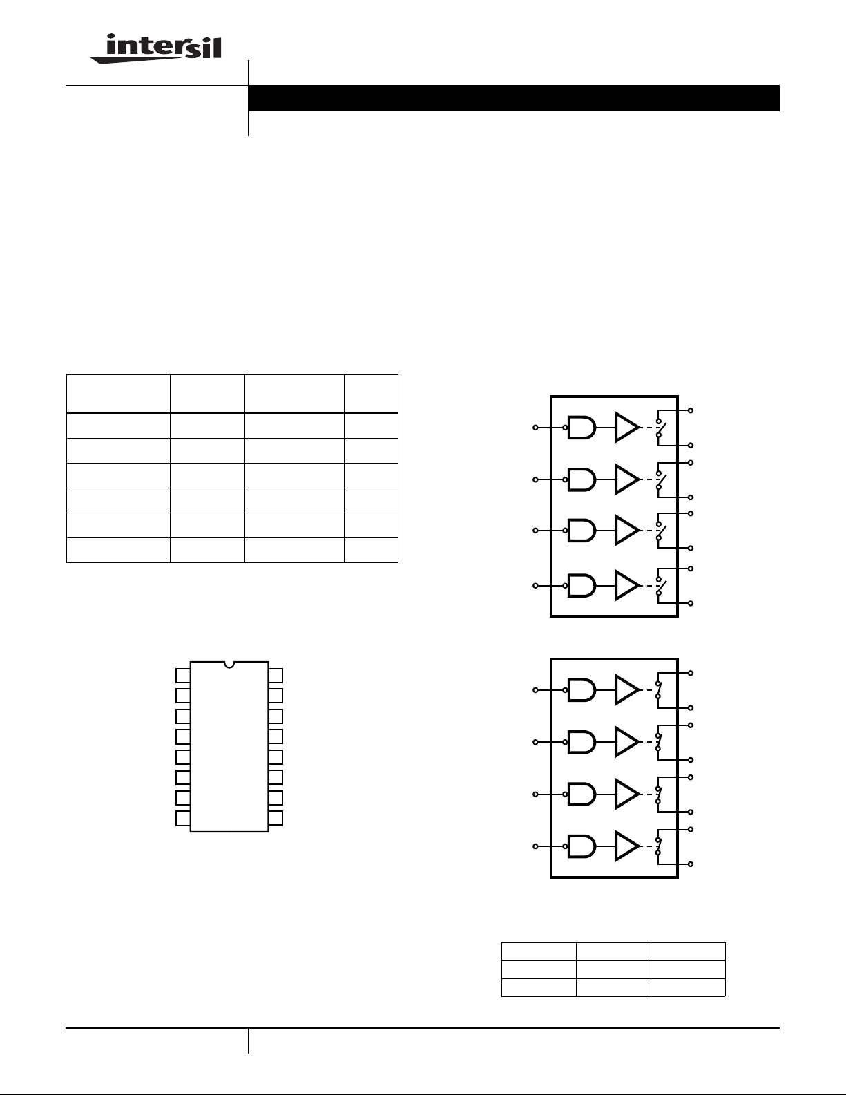
Ordering Information
TEMP.
PART NUMBER
RANGE (oC) PACKAGE
DG201AAK -55 to 125 16 Ld CERDIP F16.3
DG201ABK -25 to 85 16 Ld CERDIP F16.3
DG201ACJ 0 to 70 16 Ld PDIP E16.3
DG201ACY 0 to 70 16 Ld SOIC M16.3
DG202AK -55 to 125 16 Ld CERDIP F16.3
DG202CJ 0 to 70 16 Ld PDIP E16.3
PKG.
NO.
Pinout
DG201A, DG202
(CERDIP, PDIP, SOIC)
TOP VIEW
File Number
3117.2
Features
• Input Signal Range. . . . . . . . . . . . . . . . . . . . . . . . . . ±15V
•Low r
(Max). . . . . . . . . . . . . . . . . . . . . . . . . . 175Ω
DS(ON)
• TTL, CMOS Compatible
• Latch-Up Proof
• True Second Source
• Maximum Supply Ratings. . . . . . . . . . . . . . . . . . . . . . 44V
• Logic Inputs Accept Negative Voltages
Functional Block Diagrams
DG201A
S
IN
1
IN
2
IN
3
IN
4
DG202
1
D
1
S
2
D
2
S
3
D
3
S
4
D
4
IN
D
S
GND
S
D
IN
1
1
2
1
3
1
4
V-
5
6
4
7
4
8
4
16
15
14
13
12
11
10
9
IN
2
D
2
S
2
V+ (SUB-
-
STRATE)
NC
S
3
D
3
IN
3
IN
1
IN
2
IN
3
IN
4
SWITCHES SHOWN FOR LOGIC “1” INPUT
S
1
D
1
S
2
D
2
S
3
D
3
S
4
D
4
TRUTH TABLE
LOGIC DG201A DG202
0 ON OFF
1 OFF ON
Logic “0” ≤0.8V, Logic “1” ≥ 2.4V
4-1
CAUTION: These devices are sensitive to electrostatic discharge; follow proper IC Handling Procedures.
http://www.intersil.com or 407-727-9207 | Copyright © Intersil Corporation 1999
DG201A, DG202
Absolute Maximum Ratings Thermal Information
V+ to V- . . . . . . . . . . . . . . . . . . . . . . . . . . . . . . . . . . . . . . . . . . . 44V
V- to Ground. . . . . . . . . . . . . . . . . . . . . . . . . . . . . . . . . . . . . . . .-25V
VIN to Ground (Note 1) . . . . . . . . . . . . . . . . . . .(V-) -2V to (V+) +2V
VS or VD to V+ (Note 1). . . . . . . . . . . . . . . . . . . . . . . . +2 to (V-) -2V
VS or VD to V- (Note 1) . . . . . . . . . . . . . . . . . . . . . . . -2 to (V+) +2V
Current, any Terminal Except S or D . . . . . . . . . . . . . . . . . . . . 30mA
Continuous Current, S or D . . . . . . . . . . . . . . . . . . . . . . . . . . . 20mA
Peak Current, S or D (Pulsed 1ms, 10% Duty Cycle Max) . . . . . 70mA
Operating Conditions
Temperature Range
“A” Suffix. . . . . . . . . . . . . . . . . . . . . . . . . . . . . . . . -55oC to 125oC
“B” Suffix. . . . . . . . . . . . . . . . . . . . . . . . . . . . . . . . . -25oC to 85oC
“C” Suffix . . . . . . . . . . . . . . . . . . . . . . . . . . . . . . . . . .0oC to 70oC
CAUTION: Stresses above those listed in “Absolute Maximum Ratings” may cause permanent damage to the device. This is a stress only rating and operationofthe
device at these or any other conditions above those indicated in the operational sections of this specification is not implied.
NOTES:
1. Signals on VS, VD, or VIN exceeding V+ or V- will be clamped by internal diodes. Limit forward diode current to maximum current ratings.
2. θJA is measured with the component mounted on an evaluation PC board in free air.
Thermal Resistance (Typical, Note 2) θJA (oC/W) θJC (oC/W)
CERDIP Package. . . . . . . . . . . . . . . . . 75 20
PDIP Package . . . . . . . . . . . . . . . . . . . 100 N/A
SOIC Package . . . . . . . . . . . . . . . . . . . 100 N/A
Maximum Junction Temperature
Ceramic Package. . . . . . . . . . . . . . . . . . . . . . . . . . . . . . . . 175oC
Plastic Package . . . . . . . . . . . . . . . . . . . . . . . . . . . . . . . . . 150oC
Maximum Storage Temperature Range. . . . . . . . . . -65oC to 150oC
Maximum Lead Temperature (Soldering 10s) . . . . . . . . . . . . 300oC
(SOIC - Lead Tips Only)
Electrical Specifications V+ = 15V, V- = -15V, GND = 0V, T
PARAMETER TEST CONDITIONS
DYNAMIC CHARACTERISTICS
Turn-ON Time, t
Turn-OFF Time, t
Charge Injection, Q CL = 1nF, RS = 0, VS = 0V - 20 - - 20 - pC
OFF Isolation, OIRR VIN = 5V, RL = 75Ω, VS = 2.0V,
Crosstalk (Channel to Channel), CCRR - -90 - - -90 - dB
Source OFF Capacitance, C
Drain OFF Capacitance, C
Channel ON Capacitance,
C
D(ON)+CS(ON)
DIGITAL INPUT CHARACTERISTICS
Input Current with Voltage High, I
Input Current with Voltage Low, I
ANALOG SWITCH CHARACTERISTICS
Analog Signal Range, V
Drain-Source ON Resistance, r
Source OFF Leakage Current, I
Drain OFF Leakage Current, I
ON
OFF
S(OFF)
D(OFF)
IH
IL
ANALOG
DS(ON)
S(OFF)
D(OFF)
See Figure 1 - 480 600 - 480 - ns
See Figure 1 - 370 450 - 370 - ns
f = 100kHz
f = 140kHz, VIN = 5V, VS = VD = 0V - 5.0 - - 5.0 - pF
VIN = 2.4V -1.0 -0.0004 - -1.0 -0.0004 - µA
VIN = 15V - 0.003 1.0 - 0.003 1.0 µA
VIN = 0V -1.0 -0.0004 - -1.0 -0.0004 - µA
VD = ±10V, VIN = 0.8V (DG201A)
IS = 1mA, VIN = 2.4V (DG202)
VIN = 2.4V
(DG201A)
VIN = 0.8V
(DG202)
VS = 14V, VD = -14V - 0.01 1.0 - 0.01 5.0 nA
VS = -14V, VD = 14V -1.0 -0.02 - -5.0 -0.02 - nA
VS = -14V, VD = 14V - 0.01 1.0 - 0.01 5.0 nA
VS = 14V, VD = -14V -1.0 -0.02 - -5.0 -0.02 - nA
= 25oC
A
“A” SUFFIX “B” AND “C” SUFFIX
(NOTE 3)
TYP MAX MIN
-70--70-dB
- 5.0 - - 5.0 - pF
-16--16-pF
-15 - 15 -15 - 15 V
- 115 175 - 115 200 Ω
(NOTE 3)
TYP MAX
UNITSMIN
4-2
DG201A, DG202
Electrical Specifications V+ = 15V, V- = -15V, GND = 0V, T
PARAMETER TEST CONDITIONS
Drain ON Leakage Current, I
(Note 5)
POWER SUPPLY CHARACTERISTICS
Positive Supply Current, I+ All Channels ON or OFF - 0.9 2 - 0.9 2 mA
Negative Supply Current, I- -1 -0.3 - -1 -0.3 - mA
D(ON)
VIN = 0.8V
(DG201A)
VIN = 2.4V
(DG202)
VD = VS = 14V - 0.1 1.0 - 0.1 5.0 µA
VD = VS = -14V -1.0 -0.15 - -5.0 -0.15 - µA
Electrical Specifications V+ = 15V, V- = -15V, GND = 0V, T
PARAMETER TEST CONDITIONS
DIGITAL INPUT CHARACTERISTICS
Input Current with Voltage High, I
IH
VIN = 2.4V -10 - - µA
VIN = 15V - - 10 µA
= 25oC (Continued)
A
“A” SUFFIX “B” AND “C” SUFFIX
(NOTE 3)
TYP MAX MIN
Over Operating Temperature Range
A
(NOTE 3)
“A” SUFFIX
(NOTE 3)
TYP MAX
TYP MAX
UNITSMIN
UNITSMIN
Input Current with Voltage Low, I
ANALOG SWITCH CHARACTERISTICS
Analog Signal Range, V
Drain-Source ON Resistance, r
Source OFF Leakage Current, I
Drain OFF Leakage Current, I
Drain ON Leakage Current, I
NOTES:
3. Typical values are for design aid only, not guaranteed and not subject to production testing.
4. The algebraic convention whereby the most negative value is a minimum, and the most positive is a maximum, is used in this data sheet.
5. I
is leakage from driver into ON switch.
D(ON)
ANALOG
IL
DS(ON)
S(OFF)
D(OFF)
(Note 5) VIN = 0.8V (DG201A)
D(ON)
VIN = 0V -10 - - µA
-15 - 15 V
VD = ±10V, VIN = 0.8V (DG201A)
IS = 1mA, VIN = 2.4V (DG202)
VIN = 2.4V (DG201A)
VIN = 0.8V (DG202)
VIN = 2.4V (DG202)
VS = 14V, VD = -14V - - 100 nA
VS = -14V, VD = 14V -100 - - nA
VS = -14V, VD = 14V - - 100 nA
VS = 14V, VD = -14V -100 - - nA
VD = VS = 14V - - 200 µA
VD = VS = -14V -200 - - µA
- - 250 Ω
4-3

Test Circuits and Waveforms
LOGIC†
tr < 20ns
t
f
SWITCH
SWITCH
OUTPUT
INPUT
< 20ns
INPUT
3V
V
S
†Logic shown for DG201A, invert for DG202.
LOGIC “0” = SWITCH ON
50%
90%
t
ON
t
OFF
DG201A, DG202
VO = V
SWITCH
INPUT
90%
LOGIC
INPUT
V
= 2V
S
S
RL + r
S
1
IN
1
R
L
DS(ON)
GND
15V
-15V
V+
D
1
(REPEAT TEST FOR
IN
V-
R
L
1kΩ
, IN3 AND IN4)
2
SWITCH
OUTPUT
C
L
35pF
V
O
FIGURE 1. tON AND t
R
S
S
X
V
S
D
X
IN
X
OFF
CL = 1nF
NOTES:
6. ∆VO = Measured voltage error due to charge injection.
7. The error in coulombs is Q = CL x ∆VO.
FIGURE 2. CHARGE INJECTION TEST CIRCUIT AND MEASUREMENT POINTS
+15V
C
SIGNAL
GENERATOR
V+
V
S
SWITCHING TEST CIRCUIT AND MEASUREMENT POINTS
V
O
SWITCH
OUTPUT
IN
X
ON
SIGNAL
GENERATOR
C
3
OFF
+15V
V
S1
V+
∆V
O
ON
V
D1
50Ω
V
S
ANALYZER
CHAN A
CHAN B
C = 0.001µF||0.1µF
Chip Capacitors
FIGURE 3. OFF ISOLATION TEST CIRCUIT
V
S
IN
X
V
D
GND
R
L
V-
C
-15V
OIRR 20Log
=
V
--------
V
V
IN
ANALYZER
CHAN A
CHAN B
S
C = 0.001µF||0.1µF
Chip Capacitors
D
0V,
2.4V
R
L
IN
V
1
D2
GND
IN
2
V
S2
V-
C
-15V
CCRR 20 Log
=
0V, 2.4V
NC
V
S
1
-----------
V
2
D
FIGURE 4. CHANNEL TOCHANNEL CROSSTALK TEST
CIRCUIT
4-4
Dual-In-Line Plastic Packages (PDIP)
DG201A, DG202
N
D1
-C-
E1
-B-
A1
A2
E
A
L
e
C
C
L
e
A
C
e
B
INDEX
AREA
BASE
PLANE
SEATING
PLANE
D1
B1
1 2 3 N/2
-AD
e
B
0.010 (0.25) C AM BS
NOTES:
1. Controlling Dimensions:INCH. Incase ofconflict betweenEnglish and
Metric dimensions, the inch dimensions control.
2. Dimensioning and tolerancing per ANSI Y14.5M-1982.
3. Symbols are defined in the “MO Series SymbolList”inSection 2.2 of
Publication No. 95.
4. Dimensions A, A1andL are measuredwiththe package seatedinJEDEC seating plane gauge GS-3.
5. D, D1, and E1 dimensions do notincludemoldflash or protrusions.
Mold flash or protrusions shall not exceed 0.010 inch (0.25mm).
6. E and aremeasuredwith theleadsconstrained to beperpendic-
e
A
ular to datum .
-C-
7. eBand eCare measuredat the leadtips with theleads unconstrained.
eC must be zero or greater.
8. B1 maximum dimensionsdo not include dambarprotrusions. Dambar
protrusions shall not exceed 0.010 inch (0.25mm).
9. N is the maximum number of terminal positions.
10. Corner leads (1, N, N/2 and N/2 + 1)forE8.3,E16.3, E18.3, E28.3,
E42.6 will have a B1 dimension of 0.030 - 0.045 inch (0.76 - 1.14mm).
E16.3 (JEDEC MS-001-BB ISSUE D)
16 LEAD DUAL-IN-LINE PLASTIC PACKAGE
INCHES MILLIMETERS
SYMBOL
A - 0.210 - 5.33 4
A1 0.015 - 0.39 - 4
A2 0.115 0.195 2.93 4.95 -
B 0.014 0.022 0.356 0.558 B1 0.045 0.070 1.15 1.77 8, 10
C 0.008 0.014 0.204 0.355 -
D 0.735 0.775 18.66 19.68 5
D1 0.005 - 0.13 - 5
E 0.300 0.325 7.62 8.25 6
E1 0.240 0.280 6.10 7.11 5
e 0.100 BSC 2.54 BSC e
A
e
B
0.300 BSC 7.62 BSC 6
- 0.430 - 10.92 7
L 0.115 0.150 2.93 3.81 4
N16 169
NOTESMIN MAX MIN MAX
Rev. 0 12/93
4-5

DG201A, DG202
Ceramic Dual-In-Line Frit Seal Packages (CERDIP)
LEAD FINISH
c1
-A-
-B-
bbb C A - B
S
BASE
PLANE
SEATING
PLANE
S1
b2
ccc C A - BMD
D
A
A
b
e
S
S
NOTES:
1. Index area: A notch or a pin one identification mark shall be located adjacent to pin one and shall be located within the shaded
area shown. The manufacturer’s identification shall not be used
as a pin one identification mark.
2. The maximum limits of lead dimensions b and c or M shall be
measured at the centroid of the finished lead surfaces, when
solder dip or tin plate lead finish is applied.
3. Dimensions b1 and c1 apply to lead base metal only. Dimension
M applies to lead plating and finish thickness.
4. Corner leads (1, N, N/2, andN/2+1)may be configured with a
partial lead paddle. For this configuration dimension b3 replaces
dimension b2.
5. This dimension allows for off-center lid, meniscus, and glass
overrun.
6. Dimension Q shall be measured from the seating plane to the
base plane.
7. Measure dimension S1 at all four corners.
8. N is the maximum number of terminal positions.
9. Dimensioning and tolerancing per ANSI Y14.5M - 1982.
10. Controlling dimension: INCH.
-DBASE
E
D
S
S
Q
A
-CL
METAL
b1
M
(b)
SECTION A-A
α
(c)
M
eA
eA/2
aaa C A - B
M
c
D
S S
F16.3 MIL-STD-1835 GDIP1-T16 (D-2, CONFIGURATION A)
16 LEAD CERAMIC DUAL-IN-LINE FRIT SEAL PACKAGE
INCHES MILLIMETERS
SYMBOL
A - 0.200 - 5.08 -
b 0.014 0.026 0.36 0.66 2
b1 0.014 0.023 0.36 0.58 3
b2 0.045 0.065 1.14 1.65 b3 0.023 0.045 0.58 1.14 4
c 0.008 0.018 0.20 0.46 2
c1 0.008 0.015 0.20 0.38 3
D - 0.840 - 21.34 5
E 0.220 0.310 5.59 7.87 5
e 0.100 BSC 2.54 BSC eA 0.300 BSC 7.62 BSC -
eA/2 0.150 BSC 3.81 BSC -
L 0.125 0.200 3.18 5.08 -
Q 0.015 0.060 0.38 1.52 6
S1 0.005 - 0.13 - 7
o
α
90
105
o
90
o
105
aaa - 0.015 - 0.38 bbb - 0.030 - 0.76 -
ccc - 0.010 - 0.25 -
M - 0.0015 - 0.038 2, 3
N16 168
NOTESMIN MAX MIN MAX
o
Rev. 0 4/94
-
4-6

Small Outline Plastic Packages (SOIC)
DG201A, DG202
N
INDEX
AREA
123
-A-
E
-B-
SEATING PLANE
D
A
-C-
0.25(0.010) BM M
H
L
h x 45
o
α
e
B
0.25(0.010) C AM BS
M
NOTES:
1. Symbols are defined in the “MO Series Symbol List” in Section 2.2 of
Publication Number 95.
2. Dimensioning and tolerancing per ANSI Y14.5M-1982.
3. Dimension “D” does not include mold flash, protrusions or gate burrs.
Mold flash, protrusion and gate burrs shall not exceed 0.15mm (0.006
inch) per side.
4. Dimension “E” does not include interlead flash or protrusions. Interlead
flash and protrusions shall not exceed 0.25mm (0.010 inch) per side.
5. The chamfer on the body is optional. If it is not present, a visual index
feature must be located within the crosshatched area.
6. “L” is the length of terminal for soldering to a substrate.
7. “N” is the number of terminal positions.
8. Terminal numbers are shown for reference only.
9. The lead width “B”, as measured 0.36mm (0.014 inch) or greater above
the seating plane, shall not exceed a maximum value of 0.61mm (0.024
inch)
10. Controlling dimension: MILLIMETER. Converted inch dimensions are
not necessarily exact.
A1
C
0.10(0.004)
M16.3 (JEDEC MS-013-AA ISSUE C)
16 LEAD WIDE BODY SMALL OUTLINE PLASTIC PACKAGE
INCHES MILLIMETERS
SYMBOL
A 0.0926 0.1043 2.35 2.65 -
A1 0.0040 0.0118 0.10 0.30 -
B 0.013 0.0200 0.33 0.51 9
C 0.0091 0.0125 0.23 0.32 D 0.3977 0.4133 10.10 10.50 3
E 0.2914 0.2992 7.40 7.60 4
e 0.050 BSC 1.27 BSC H 0.394 0.419 10.00 10.65 -
h 0.010 0.029 0.25 0.75 5
L 0.016 0.050 0.40 1.27 6
N16 167
o
α
0
o
8
o
0
o
8
Rev. 0 12/93
NOTESMIN MAX MIN MAX
-
All Intersil semiconductor products are manufactured, assembled and tested under ISO9000 quality systems certification.
Intersil semiconductor products are sold by description only. Intersil Corporation reserves the right to make changes in circuit design and/or specifications at any time without notice. Accordingly, the reader is cautioned to verify that data sheets are current before placing orders. Information furnished by Intersil is believed to be accurate and
reliable. However, no responsibility is assumed by Intersil or its subsidiaries for its use; nor for any infringements of patents or other rights of third parties which may result
from its use. No license is granted by implication or otherwise under any patent or patent rights of Intersil or its subsidiaries.
For information regarding Intersil Corporation and its products, see web site http://www.intersil.com
Sales Office Headquarters
NORTH AMERICA
Intersil Corporation
P. O. Box 883, Mail Stop 53-204
Melbourne, FL 32902
TEL: (407) 724-7000
FAX: (407) 724-7240
4-7
EUROPE
Intersil SA
Mercure Center
100, Rue de la Fusee
1130 Brussels, Belgium
TEL: (32) 2.724.2111
FAX: (32) 2.724.22.05
ASIA
Intersil (Taiwan) Ltd.
7F-6, No. 101 Fu Hsing North Road
Taipei, Taiwan
Republic of China
TEL: (886) 2 2716 9310
FAX: (886) 2 2715 3029
 Loading...