Intersil Corporation CDP68HC68W1 Datasheet

CDP68HC68W1
March 1998
Features
• Programmable Frequency and Duty Cycle Output
• Serial Bus Input; Compatible with Motorola/Intersil
SPI Bus, Simple Shift-Register Type Interface
• 8 Lead PDIP Package
• Schmitt Trigger Clock Input
o
• 4V to 6V Operation, -40
C to 85oC Temperature Range
• 8MHz Clock Input Frequency
Pinout
CDP68HC68W1
(PDIP)
TOP VIEW
CLK
1
2
CS
3
V
T
V
4
SS
8
V
DD
7
PWM
6
SCK
5
DAT A
CMOS Serial Digital Pulse Width Modulator
Description
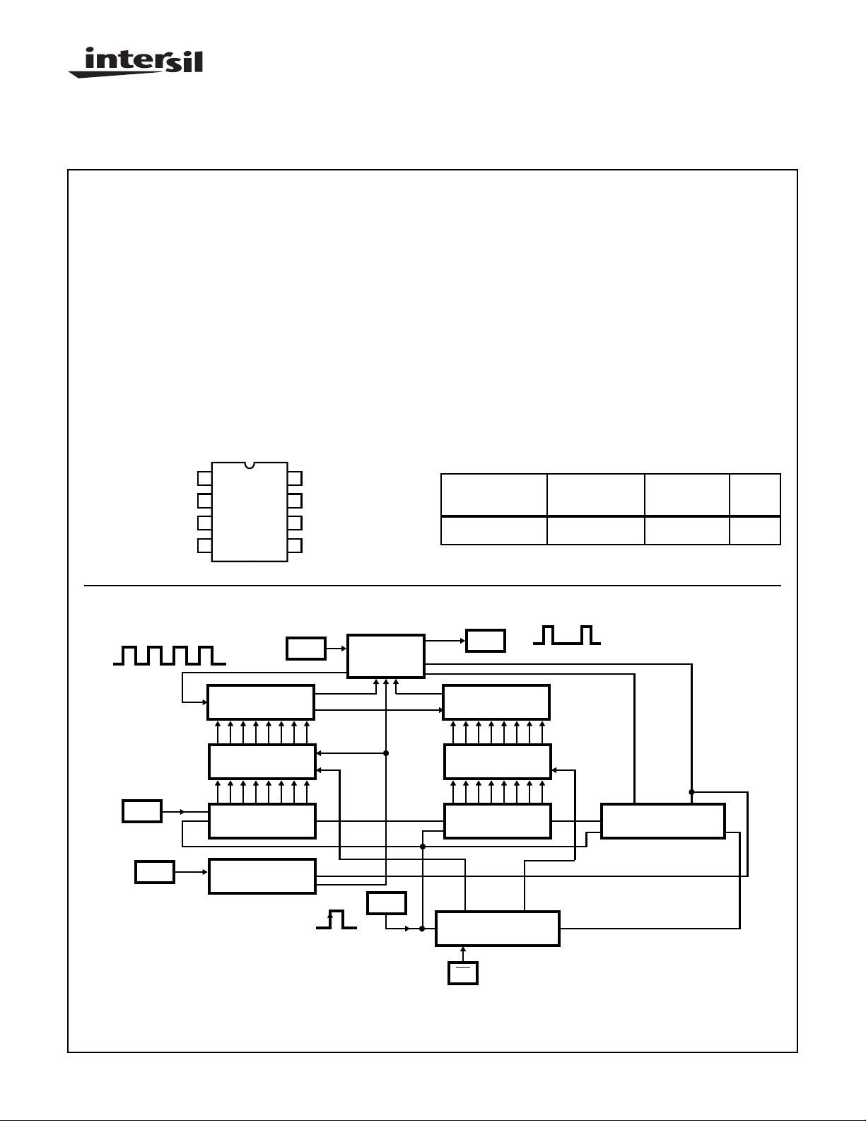
The CDP68HC68W1 modulates a clock input to supply a
variable frequency and duty-cycle output signal. Three 8-bit
registers (pulse width, frequency and control) are accessed
serially after power is applied to initialize device operation.
The value in the pulse width register selects the high
duration of the output period. The frequency register byte
divides the clock input frequency and determines the overall
output clock period. The input clock can be further divided by
two or a low power mode may be selected by the lower two
bits in the control register. A comparator circuit allows
threshold control by setting the output low if the input at the
V
pin rises above 0.75V. The CDP68HC68W1 is supplied in
T
an 8 lead PDIP package (E suffix).
Ordering Information
TEMP. RANGE
PART NUMBER
CDP68HC68W1E -40 to 85 8 Ld PDIP E8.3
(oC) PACKAGE
PKG.
NO.
Block Diagram
DAT A
V
T
8 - STAGE RIPPLE
COUNTER
PULSE - WIDTH
DATA REGISTER
8 - STAGE SHIFT
REGISTER
V
T
COMPARATOR
CLK
RESET
LOAD
INPUT CLK
MODULATOR
LOGIC
SCK
PWM
8 - STAGE RIPPLE
COUNTER
FREQUENCY
DATA REGISTER
8 - STAGE SHIFT
REGISTER
168
5 - STAGE 24 - STATE
COMPARATOR
CS
LOAD
24
CONTROL REGISTER
2 - STAGE SHIFT
LOAD
CAUTION: These devices are sensitive to electrostatic discharge; follow proper IC Handling Procedures.
http://www.intersil.com or 407-727-9207
| Copyright © Intersil Corporation 1999
1
File Number 1919.3

CDP68HC68W1
Absolute Maximum Ratings Thermal Information
DC Supply Voltage Range, (VDD) . . . . . . . . . . . . . . . . -0.5V to +7V
(Voltage Referenced to VSS Terminal)
Input Voltage Range, All Inputs . . . . . . . . . . . . .-0.5V to VDD +0.5V
DC Input Current, Any One Input. . . . . . . . . . . . . . . . . . . . . . . . .±10mA
Operating Conditions
Temperature Range (TA) . . . . . . . . . . . . . . . . . . . . . . -40oC to 85oC
TA = Full Package Temperature Range (All Package Types)
CAUTION: Stresses above those listed in “Absolute Maximum Ratings” may cause permanent damage to the device. This is a stress only rating and operation
of the device at these or any other conditions above those indicated in the operational sections of this specification is not implied.
NOTE:
1. θJA is measured with the component mounted on an evaluation PC board in free air.
DC Electrical Specifications
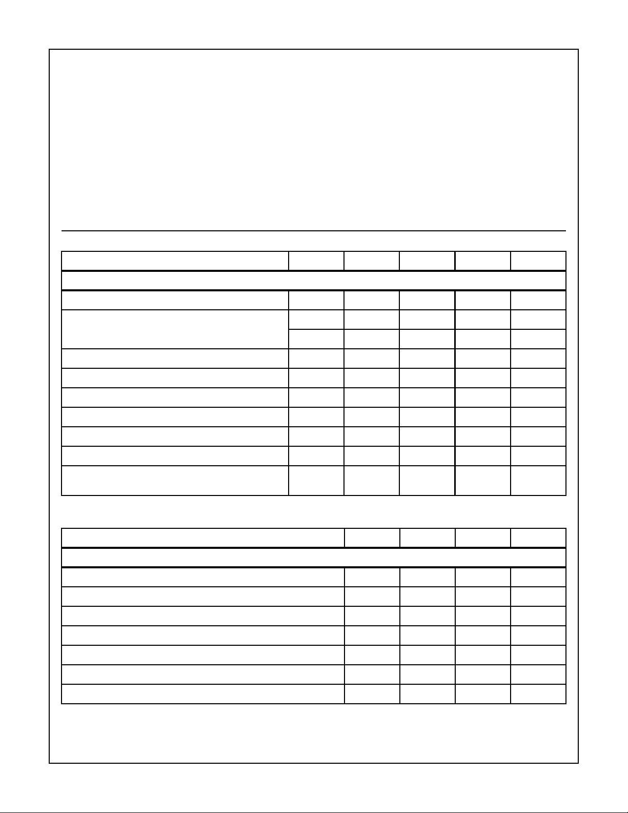
PARAMETER SYMBOL MIN TYP MAX UNITS
CDP68HC68W1, VDD = 5V ±10%, VSS = 0V, TA = -40oC to 85oC
DC Operating Voltage Range - 4 - 6 V
Thermal Resistance (Typical, Note 1) θJA (oC/W)
PDIP Package. . . . . . . . . . . . . . . . . . . . . . . . . . . . . 99
Device Dissipation Per Output Transistor . . . . . . . . . . . . . . .100mW
Maximum Storage Temperature Range (T
) . . . .-65oC to 150oC
STG
Maximum Lead Temperature (During Soldering) . . . . . . . . . . 265oC
At Distance 1/16 ±1/32 in. (1.59 ± 0.79mm)
From Case for 10s Max
Input Voltage Range (Except VT Pin) V
VT Pin Output Voltage Threshold V
Device Current in “Power Down” Mode, Clock Disabled I
Low Level Output Voltage (IOL = 1.6mA) V
High Level Output Voltage (IOH = -1.6mA) V
Input Leakage Current I
Operating Device Current (f
= 1MHz) I
CLK
OPER
Clock Input Capacitance
(VIN = 0V, f
= 1MHz, TA = 25oC)
CLK
IH
V
IL
IT
PD
OL
OH
IN
C
IN
0.7•V
DD
-0.3 - 0.3•V
0.4 - 0.15•V
-V
+0.3V V
DD
DD
DD
--1µA
- - 0.4 V
VDD - 0.4V - - V
--±1 µA
--1mA
- - 10 pF
Control Timing
PARAMETER SYMBOL MIN MAX UNITS
CDP68HC68W1, VDD = 5V ±10%, VSS = 0V, TA = -40oC to 85oC
Clock Frequency F
Cycle Time t
Clock to PWM Out t
Clock High Time t
Clock Low Time t
Rise Time (20% VDD to 70% VDD)t
Fall Time (70% VDDto 20% VDD)t
CLK
CYC
PWMO
CLKH
CLKL
R
F
DC 8.0 MHz
--ns
- 125 ns
50 - ns
50 - ns
- 100 ns
- 100 ns
V
V
2

CDP68HC68W1
SPI Interface Timing
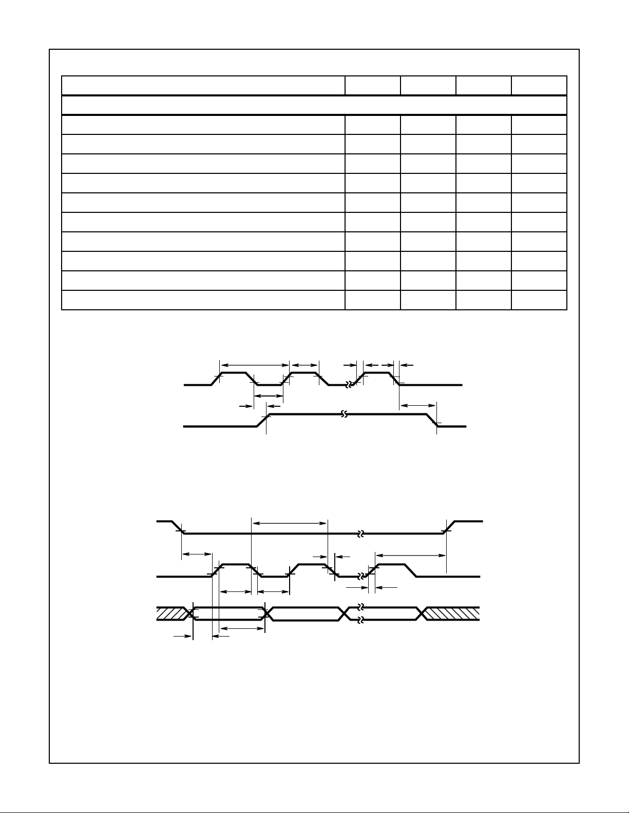
PARAMETER SYMBOL MIN MAX UNITS
CDP68HC68W1, VDD = 5V ±10%, VSS = 0V, TA = -40oC to 85oC
Serial Clock Frequency f
Cycle Time t
Enable Lead Time t
Enable Lag Time t
Serial Clock (SCK) High Time t
Serial Clock (SCK) Low Time t
Data Setup Time t
Data Hold Time t
Fall Time (70% VDD to 20% VDD, CL = 200pF) t
Rise Time (20% VDD to 70% VDD, CL = 200pF) t
t
CLKH
t
R
CLK
t
PWMO
t
CYC
t
CLKL
SCK
SCYC
ELD
ELG
SH
SL
DSU
DHD
SCKF
SCKR
DC 2.1 MHz
480 - ns
240 - ns
- 200 ns
190 - ns
190 - ns
100 - ns
100 - ns
- 100 ns
- 100 ns
t
F
t
PWMO
CS
(INPUT)
SCK
(INPUT)
DAT A
(INPUT)
PWM
FIGURE 1. PWM TIMING
t
SCYC
t
ELD
t
DSU
t
SH
MSB LSB
t
DHD
t
SCKF
t
SL
FIGURE 2. SERIAL PERIPHERAL INTERFACE TIMING
t
t
SCKR
ELG
3
 Loading...