Intersil Corporation CDP68HC68T1 Datasheet
August 1997
CDP68HC68T1
CMOS Serial Real-Time Clock With
RAM and Power Sense/Control
Features
• SPI (Serial Peripheral Interface)
• Full Clock Features
- Seconds, Minutes, Hours (12/24, AM/PM), Day of
Week, Date, Month, Year (0-99), Automatic Leap Year
• 32 Word x 8-Bit RAM
• Seconds, Minutes, Hours Alarm
• Automatic Power Loss Detection
• Low Minimum Standby (Timekeeping) Voltage. . . 2.2V
• Selectable Crystal or 50/60Hz Line Input
• Buffered Clock Output
• Battery Input Pin that Powers Oscillator and also
Connects to V
Pin When Power Fails
DD
• Three Independent Interrupt Modes
- Alarm
- Periodic
- Power-Down Sense
Description
The CDP68HC68T1 Real-Time Clock provides a
time/calendar function, a 32 byte static RAM, and a 3 wire
Serial Peripheral Interface (SPI Bus). The primary function of
the clock is to divide down a frequency input that can be
supplied by the on-board oscillator in conjunction with an
external crystal or by an external clock source. The internal
oscillator can operate with a 32KHz, 1MHz, 2MHz, or 4MHz
crystal. An external clock source with a 32KHz, 1MHz,
2MHz, 4MHz, 50Hz or 60Hz frequency can be used to drive
the CDP68HC68T1. The time registers hold seconds,
minutes, and hours, while the calendar registers hold day-ofweek, date, month, and year information. The data is stored
in BCD format. In addition, 12 or 24 hour operation can be
selected. In 12 hour mode, an AM/PM indicator is provided.
The T1 has a programmable output which can provide one
of seven outputs for use elsewhere in the system.
Computer handshaking is controlled with a “wired-OR”
interrupt output. The interrupt can be programmed to provide
a signal as the result of: 1) an alarm programmed to occur at
a predetermined combination of seconds, minutes, and
hours; 2) one of 15 periodic interrupts ranging from subsecond to once per day frequency; 3) a power fail detect.
The PSE output and the V
power control. The
CPUR output is available to reset the
processor under power-down conditions.
under software control and can also be activated via the
CDP68HC68T1’s watchdog. If enabled, the watchdog
requires a periodic toggle of the CE pin without a serial
transfer.
input are used for external
SYS
CPUR is enabled
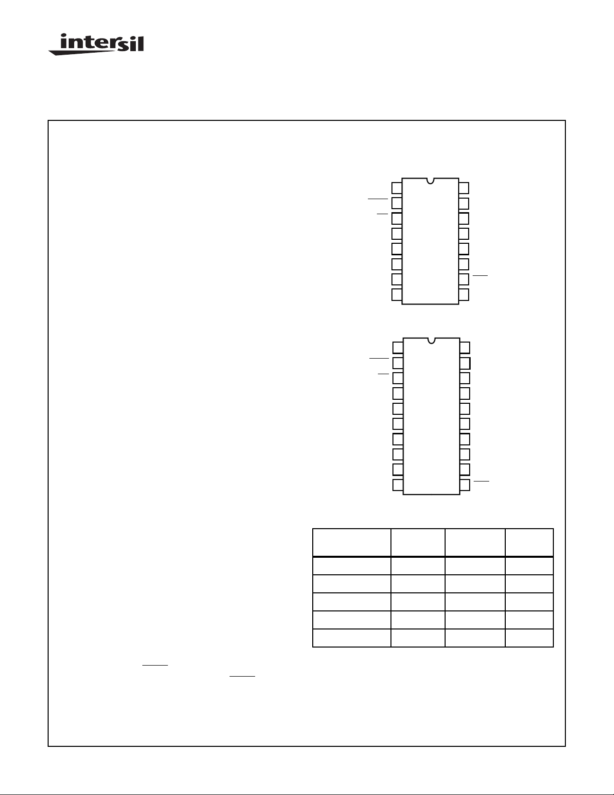
Pinouts
CDP68HC68T1 (PDIP, SBDIP, SOIC)
TOP VIEW
CLKOUT
CPUR
INT
SCK
MOSI
MISO
CE
V
SS
CLK OUT
CPUR
INT
NC
SCK
MOSI
MISO
CE
V
SS
PSE
1
2
3
4
5
6
7
8
CDP68HC68T1 (SOIC)
TOP VIEW
1
2
3
4
5
6
7
8
9
10
16
V
XTAL OUT
15
XTAL IN
14
V
13
V
12
LINE
11
POR
10
PSE
9
20
19
18
17
16
15
14
13
12
11
DD
BATT
SYS
VDD
XTAL OUT
XTAL IN
NC
V
BATT
V
SYS
NC
NC
LINE
POR
Ordering Information
TEMP.
PART NUMBER
CDP68HC68T1E -40 to 85 16 Ld PDIP E16.3
CDP68HC68T1D -40 to 85 16 Ld SBDIP D16.3
CDP68HC68T1M -40 to 85 20 Ld SOIC M20.3
CDP68HC68T1M2 -40 to 85 16 Ld SOIC M16.3
CDP68HC68T1W -40 to 85 DIE
NOTE: Pin number references throughout this specification refer to
the 16 lead PDIP/SBDIP/SOIC. See pinouts for cross reference.
RANGE (oC) PACKAGE
PKG.
NO.
CAUTION: These devices are sensitive to electrostatic discharge; follow proper IC Handling Procedures.
http://www.intersil.com or 407-727-9207
| Copyright © Intersil Corporation 1999
1
File Number 1547.3
CDP68HC68T1
Absolute Maximum Ratings Thermal Information
Supply Voltage, VDD. . . . . . . . . . . . . . . . . . . . . . . . . . . -0.5V to +7V
Input Voltage, VIN. . . . . . . . . . . . . . . . . . . . VSS -0.3V to VDD +0.3V
Current Drain Per Input Pin Excluding VDD and VSS, I . . . . . .10mA
Current Drain Per Output Pin, I. . . . . . . . . . . . . . . . . . . . . . . . .40mA
Operating Conditions
Voltage Range . . . . . . . . . . . . . . . . . . . . . . . . . . . . . +3.0V to +6.0V
Standby (Timekeeping) Voltage . . . . . . . . . . . . . . . . +2.2V to +6.0V
Temperature Range
CDP68HC68T1D (SBDIP Package). . . . . . . . . . . -55oC to 125oC
CDP68HC68T1E (PDIP Package) . . . . . . . . . . . . . -40oC to 85oC
CDP68HC68T1M/M2 (SOIC Packages). . . . . . . . . -40oC to 85oC
Input High Voltage . . . . . . . . . . . . . . . . . . . . . . . (0.7 x VDD) to V
Input Low Voltage. . . . . . . . . . . . . . . . . . . . . . . . . .0V to (0.3 x VDD)
Serial Clock Frequency (f
CAUTION: Stresses above those listed in “Absolute Maximum Ratings” may cause permanent damage to the device. This is a stress only rating and operation
of the device at these or any other conditions above those indicated in the operational sections of this specification is not implied.
NOTE:
1. θJA is measured with the component mounted on an evaluation PC board in free air.
) . . . . . . . . . . . . . . . . . +3.0V to +6.0V
SCK
Thermal Resistance (Typical, Note 1) θJA (oC/W) θJC (oC/W)
16 Ld PDIP . . . . . . . . . . . . . . . . . . . . . 90 N/A
16 Ld SOIC . . . . . . . . . . . . . . . . . . . . . 100 N/A
20 Ld SOIC . . . . . . . . . . . . . . . . . . . . . 100 N/A
16 Ld SBDIP . . . . . . . . . . . . . . . . . . . . 75 24
Maximum Junction Temperature (Hermetic) . . . . . . . . . . . . . . . 175oC
Maximum Junction Temperature (Plastic) . . . . . . . . . . . . . . . 150oC
Maximum Storage Temperature Range (T
) . . . .-65oC to 150oC
STG
Maximum Lead Temperature (Soldering 10s) . . . . . . . . . . . . . 300oC
(SOIC, Lead Tips Only)
DD
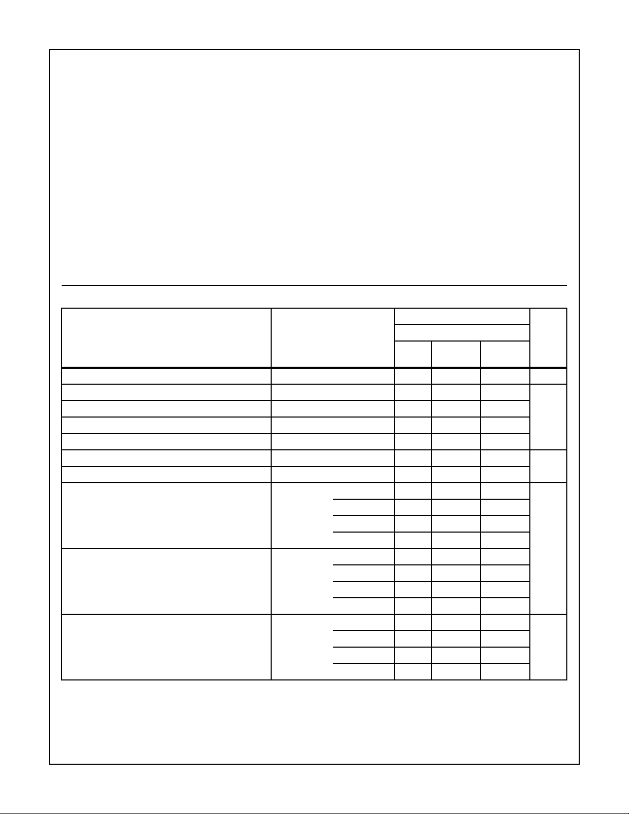
Static Electrical Specifications At T
PARAMETER CONDITIONS
Quiescent Device Current I
Output Voltage High Level V
Output Voltage Low Level V
Output Voltage High Level V
Output Voltage Low Level V
Input Leakage Current I
Three-State Output Leakage Current I
Operating Current (Note 3)
(ID + IB) VDD = VB = 5V
Crystal Operation
Pin 14
External Clock (Squarewave) (Note 3)
(ID + IB) VDD= VS = 5V
Standby Current (Note 3) I
VS = 3V
Crystal Operation
= -40oC to +85oC, VDD = V
A
DD
OH
OL
OH
OL
IN
OUT
B
IOH = -1.6mA, VDD = 4.5V 3.7 - IOL = 1.6mA, VDD = 4.5V
IOH≤ 10µA, VDD = 4.5V 4.4 - IOL≤ 10µA, VDD = 4.5V
= 5V ±5%, except as noted.
BATT
LIMITS
CDP68HC68T1
(NOTE 2)
MIN
TYP MAX
-1 10µA
-
-
- 0.4
- 0.1
-- ±1
--±10
32kHz - 0.08 0.01
1MHz - 0.5 0.6
2MHz - 0.7 0.84
4MHz - 1 1.2
32kHz - 0.02 0.024
1MHz - 0.1 0.12
2MHz - 0.2 0.24
4MHz - 0.4 0.5
32kHz - 20 25
1MHz - 200 250
2MHz - 300 360
4MHz - 500 600
UNITS
V
µA
mA
µA
2
CDP68HC68T1
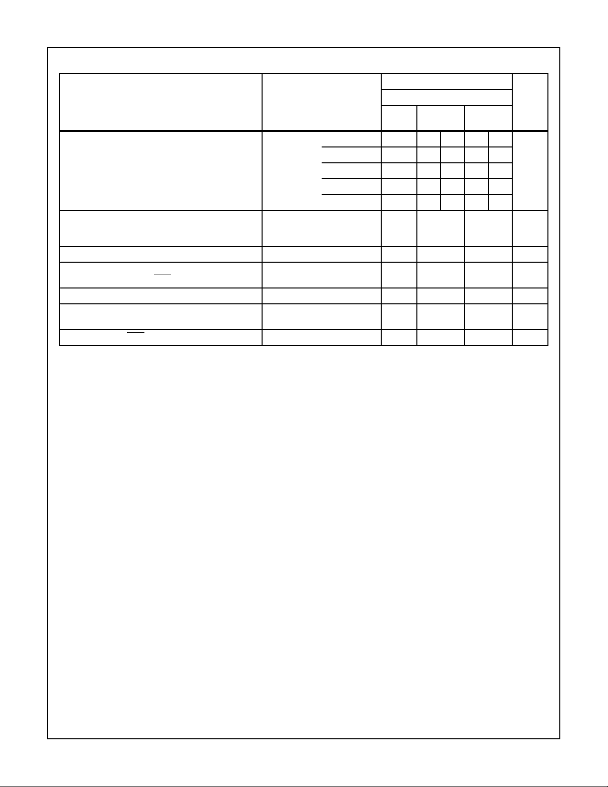
Static Electrical Specifications At T
PARAMETER CONDITIONS
Operating Current (Note 3)
VDD = 5V, VB = 3V
Crystal Operation
Standby Current (Note 3) I
VB = 2.2V
Crystal Operation
Input Capacitance C
Maximum Rise and Fall Times tr, t
(Except XTAL Input and POR Pin 10)
Input Voltage (Line Input Pin Only, Power Sense Mode) 0 10 12 V
V
> V
SYS
(For VB Not Internally Connected to VDD)
Power-On Reset (POR) Pulse Width 100 75 - ns
NOTES:
2. Typical values are for TA = 25oC and nominal VDD.
3. Clock out (Pin 1) disabled, outputs open circuited. No serial access cycles.
B
= -40oC to +85oC, VDD = V
A
B
IN
f
V
T
VIN = 0, TA = 25oC--2pF
= 5V ±5%, except as noted. (Continued)
BATT
LIMITS
CDP68HC68T1
(NOTE 2)
MIN
32kHz - 25 15 30 20
1MHz - 0.08 0.15 0.1 0.18
2MHz - 0.15 0.25 0.18 0.3
4MHz - 0.3 0.4 0.36 0.5
32kHz - 10 12 µA
-- 2µs
- 0.7 - V
TYP MAX
I
DIBIDIS
UNITS
mA
3
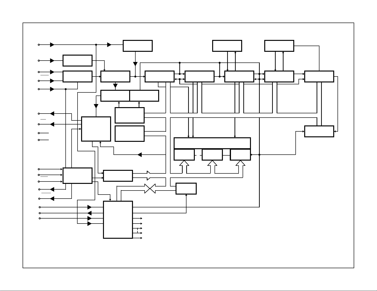
Functional Block Diagram
CE
LINE
50/60Hz
XTAL IN
XTAL OUT
V
BATT
CLOCK
OUT
INT
V
DD
V
SS
OSCILLATOR
CLOCK
LOGIC
PRESCALE SECOND MINUTE HOUR
PRESCALE
SELECT
AND
INT
4
LINE
V
SYS
POR
PSE
CPUR
POWER
SENSE
CONTROL
INT STATUS
REGISTER
FREEZE
CIRCUIT
CLOCK
CONTROL
REGISTER
INTERRUPT
CONTROL
REGISTER
CLOCK
SELECT
SECOND
LATCH
32 X 8
RAM
AM - PM AND
HOUR LOGIC
COMPARATOR
MINUTE
LATCH
8-BIT DATA BUS
HOUR
LATCH
CALENDAR
LOGIC
DAY/DAY
OF WEEK
MONTH
CDP68HC68T1
YEAR
SCK
MISO
MOSI
SERIAL
INTERFACE
FIGURE 1. REAL TIME CLOCK FUNCTIONAL DIAGRAM
CDP68HC68T1
0
32 RAM LOCATIONS
31
32
CLOCK/CALENDAR
50
51
13 BYTES UNUSED
63
TEST MODE
R = READABLE W = WRITABLE
$00
$1F
$20
$32
$33
$3F
$5585
32
33
34
35
36
37
38
39
40
41
42
43
44
45
46
47
48
49
50
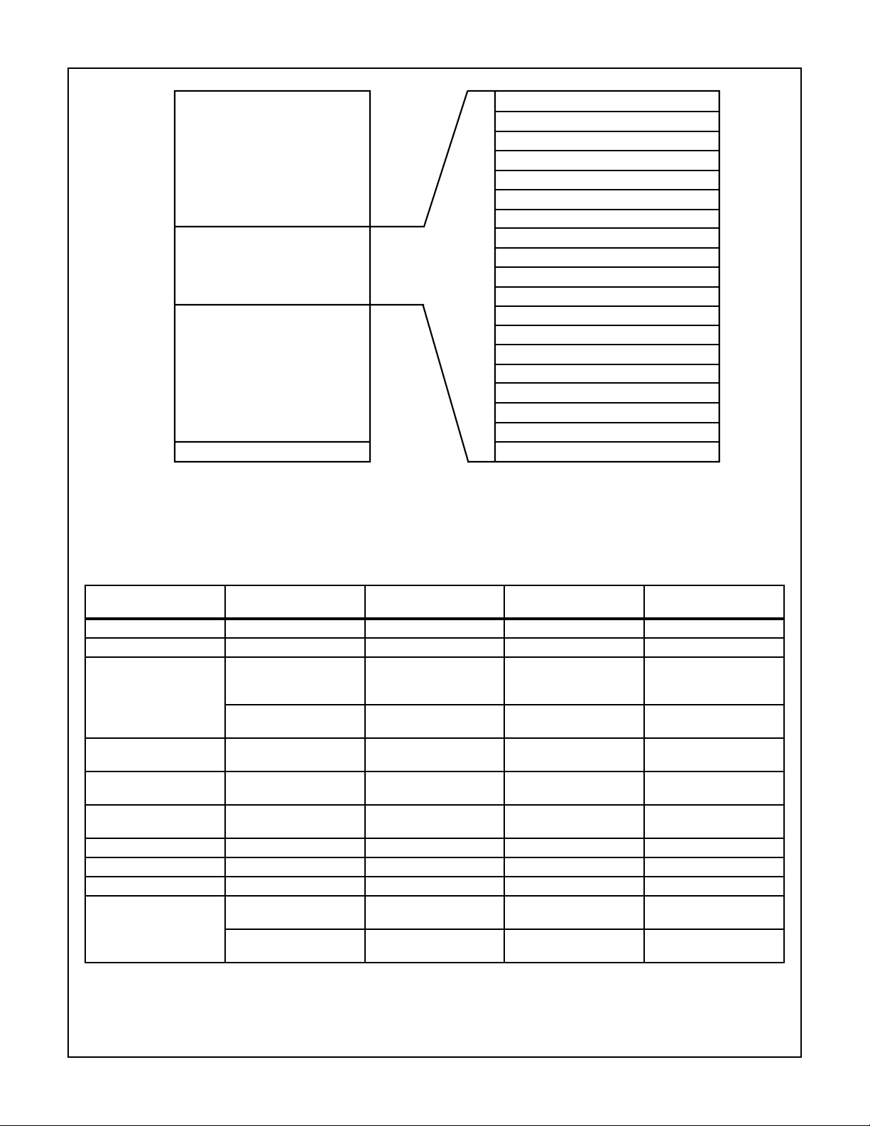
FIGURE 2. ADDRESS MAP
SECONDS
MINUTES
HOURS
DAY OF WEEK
DATE
MONTH
YEARS
NOT USED
SEC ALARM
MIN ALARM
HRS ALARM
NOT USED
NOT USED
NOT USED
NOT USED
NOT USED
STATUS REGISTER
CONTROL REGISTER
INTERRUPT CONTROL REGISTER
R, W
R, W
R, W
R, W
R, W
R, W
R, W
R, W
R, W
$20
$21
$22
$23
$24
$25
$26
$27
$28
W
$29
W
$2A
W
$2B
$2C
$2D
$2E
$2F
$30
R
$31
$32
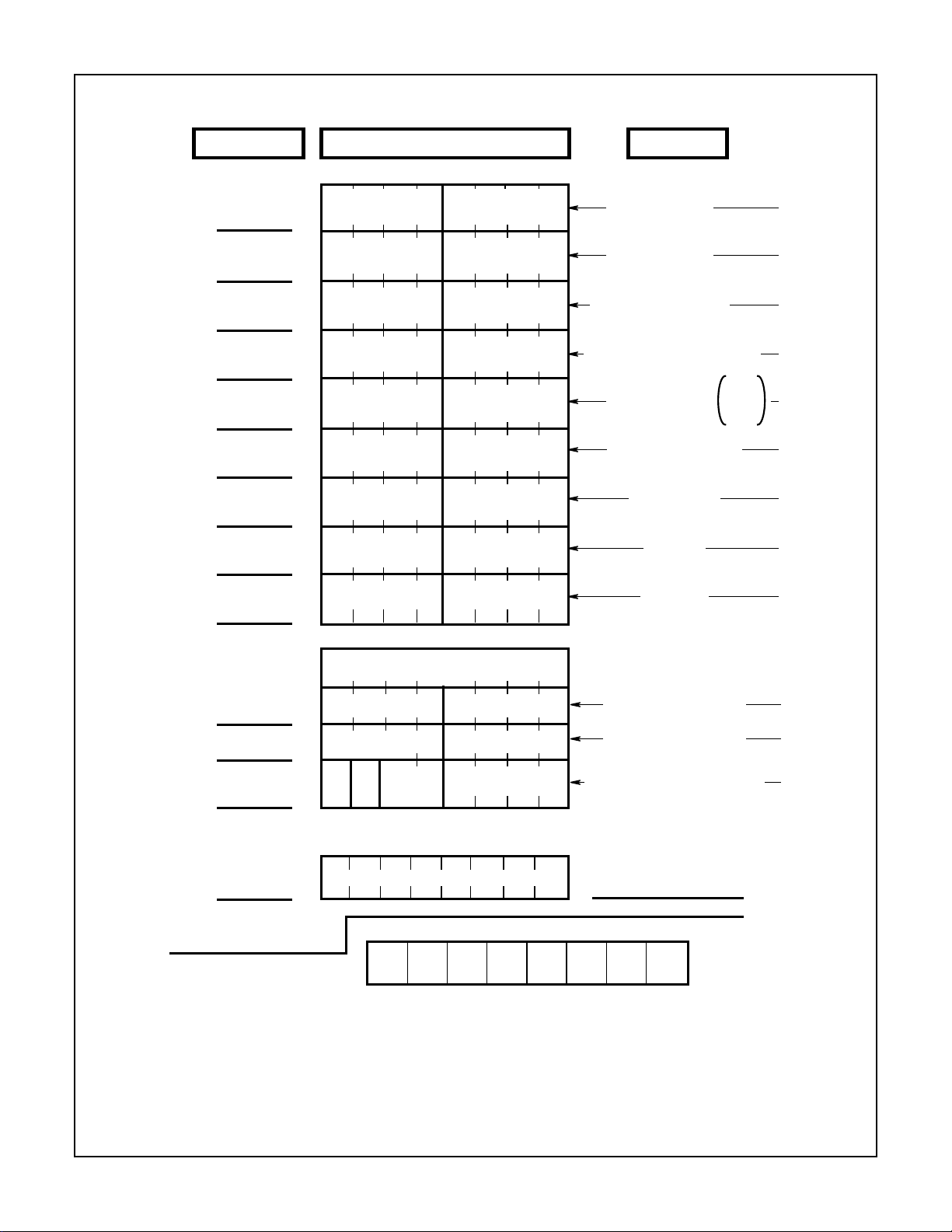
TABLE 1. CLOCK/CALENDAR AND ALARM DATA MODES
ADDRESS LOCATION
(H) FUNCTION DECIMAL RANGE BCD DATA RANGE
(NOTE 4)
BCD DATE EXAMPLE
20 Seconds 0-59 00-59 18
21 Minutes 0-59 00-59 49
22 Hours
12 Hour Mode
1-12 81-92 (AM)
A1-B2 (PM)
A3
(Note 5)
Hours
0-23 00-23 15
24 Hour Mode
23 Day of the Week
1-7 01-07 03
(Sunday = 1)
24 Day of the Month
1-31 01-31 29
(Date)
25 Month
1-12 01-12 10
Jan = 1, Dec = 12
26 Years 0-99 00-99 85
28 Alarm Seconds 0-59 00-59 18
29 Alarm Minutes 0-59 00-59 49
2A Alarm Hours (Note 6)
12 Hour Mode
Alarm Hours
1-12 01-12 (AM)
23
21-32 (PM)
0-23 00-23 15
24 Hour Mode
NOTES:
4. Example: 3:49:18, Tuesday. Oct. 29,1985.
5. Most significant Bit, D7, is “0” for 24 hours, and “1” for 12 hour mode. Data Bit D5 is “1” for P.M. and ‘0” for A.M. in 12 hour mode.
6. Alarm hours. Data Bit D5 is “1” for P.M. and “0” for A.M. in 12 hour mode. Data Bits D7 and D6 are DON’T CARE.
5
CDP68HC68T1
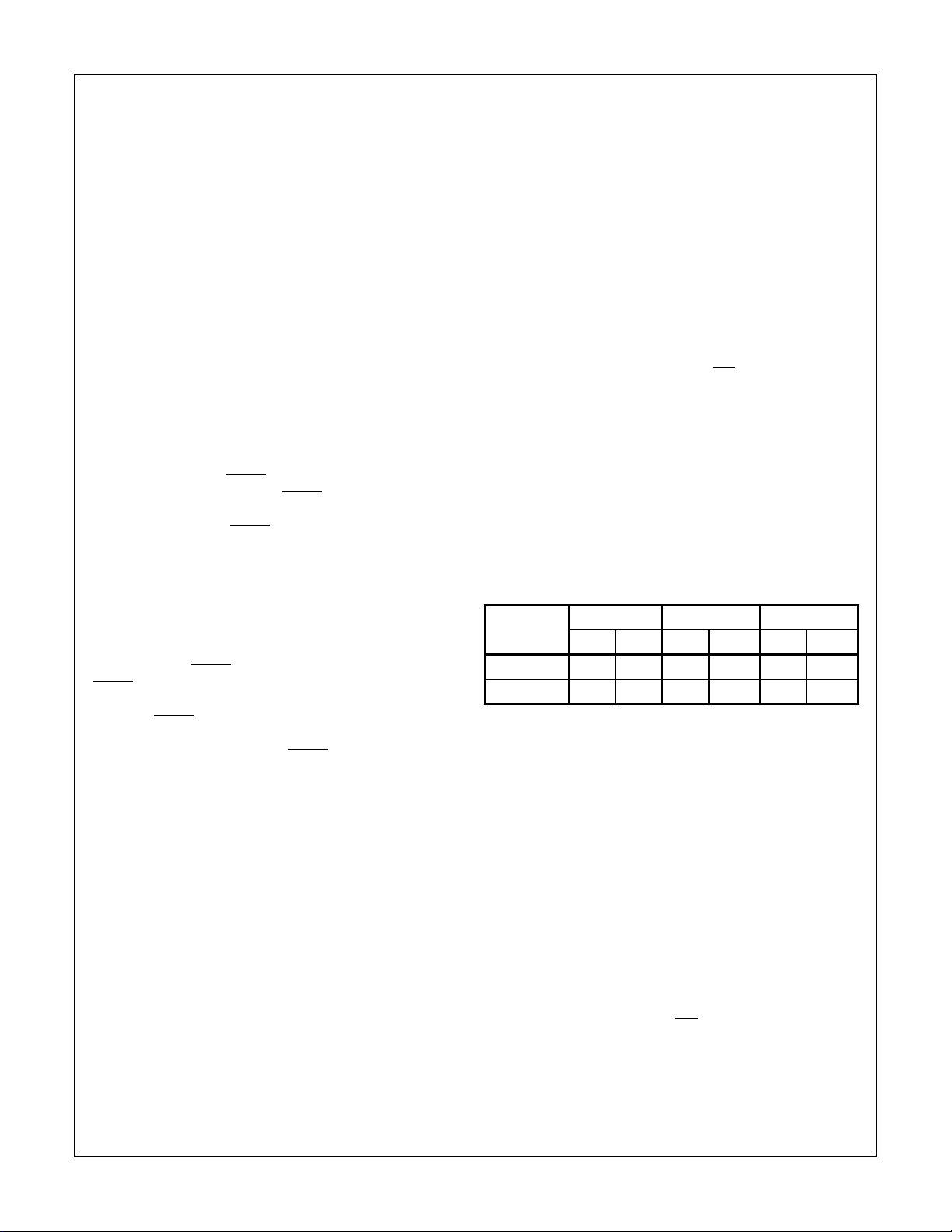
Programmers Model - Clock Registers
NAMEWRITE/READ REGISTERSHEX ADDRESS
DB7
20
21
22
23
24
25
26
31
32
TENS 0-5
TENS 0-5
12
HR
24
XXXX
76543210
76543210
PM/AM
X
TENS 0-2
TENS 0-3
TENS 0-1
TENS 0-9
X
UNITS 0-9
UNITS 0-9
UNITS 0-9
UNITS 1-7
UNITS 0-9
UNITS 0-9
UNITS 0-9
DB0
SECONDS (00-59)
MINUTES (00-59)
DB7, 1 = 12 HR., 0 = 24 HR.
DB = 1 PM, 0 = AM
HOURS (01-12 OR 00-23
DAY OF WK (01-07) SUNDAY = 1
01-28
DATE
DAY OF MONTH
MONTH (01-12) JAN = 1
DEC = 12
YEARS (00-99)
CONTROL
INTERRUPT
29
30
31
28
29
2A
30
RAM DATA BYTE
XX
765 432 1 0
NOTE: X = Don’t care writes, X = 0 when read.
WRITE ONLY REGISTERS
TENS 0-5
TENS 0-5
PM/AM
TENS 0-2
READ ONLY REGISTERS
7654321 0
D7 D6 D5 D4 D3 D2 D1 D0
HEX ADDRESS 00-1F
UNITS 0-9
UNITS 0-9
UNITS 0-9
BIT
ALARM SECONDS (00-59)
ALARM MINUTES (00-59)
ALARM HOURS (01-12 OR 00-23)
PLUS AM/PM IN 12 HR. MODE
PM = 1, AM = 0
STATUS
6
Functional Description
CDP68HC68T1
The SPI real-time clock consists of a clock/calendar and a
32 x 8 RAM. Communications is established via the SPI
(Serial Peripheral Interface) bus. In addition to the clock/calendar data from seconds to years, and system flexibility provided by the 32-byte RAM, the clock features computer
handshaking with an interrupt output and a separate squarewave clock output that can be one of 7 different frequencies.
An alarm circuit is available that compares the alarm latches
with the seconds, minutes and hours time counters and activates the interrupt output when they are equal. The clock is
specifically designed to aid in power-down/up applications
and offers several pins to aid the designer of battery backup
systems.
Mode Select
The voltage level that is present at the V
input pin at the
SYS
end of power-on-reset selects the device to be in the single
supply or battery backup mode.
Single-Supply Mode
If V
CLK OUT, PSE and
will be completely operational.
logic level at the V
CLK OUT, PSE and
down instruction, V
is a logic high when power-on-reset is completed,
SYS
CPUR will be enabled and the device
CPUR will be placed low if the
pin goes low. If the output signals
SYS
CPUR are disabled due to a power-
brought to a logic low and then to a
SYS
logic high will re-enable these outputs. An example of the
single-supply mode is where only one supply is available
and V
DD
, V
BATT
and V
are tied together to the supply.
SYS
Battery Backup Mode
If V
OUT, PSE and
CPUR low). This condition will be held until V
threshold (about 0.7V) above V
PSE and
operational. If V
outputs CLK OUT, PSE and
example of battery backup operation occurs if V
V
connected to the V
is a logic low at the end of power-on-reset, CLK
SYS
CPUR will be disabled (CLK OUT, PSE and
rises to a
. The outputs CLK OUT,
BATT
SYS
CPUR will then be enabled and the device will be
falls below a threshold above V
SYS
BATT
CPUR will be disabled. An
is tied to
and VDD is not connected to a supply when a battery is
DD
pin. (See Pin Functions, V
BATT
SYS
BATT
the
for
Battery Backup Operation.)
Clock/Calendar (See Figure 1 and Figure 2)
The clock/calendar portion of this device consists of a long
string of counters that is toggled by a 1Hz input. The 1Hz
input is generated by a prescaler driven by an on-board
oscillator that utilizes one of four possible external crystals or
that can be driven by an external clock source. The 1Hz trigger to the counters can also be supplied by a 50Hz or 60Hz
input source that is connected to the LINE input pin.
The time counters offer seconds, minutes and hours data in
12 hour or 24 hour format. An AM/PM indicator is available
that once set, toggles every 12 hours. The calendar counters
consist of day (day of week), date (day of month), month and
years information. Data in the counters is in BCD format.
The hours counter utilizes BCD for hour data plus bits for
12/24 hour and AM/PM. The 7 time counters are accessed
serially at addresses 20H through 26H. (See Table 1).
RAM
The real-time clock also has a static 32 x 8 RAM that is
located at addresses 00-1FH. Transmitting the address/control word with bit-5 low selects RAM access. Bits 0 through 4
select the RAM location.
Alarm
The alarm is set by accessing the three alarm latches and
loading the required data. The alarm latches consist of seconds, minutes and hours registers. When their outputs equal
the values in the seconds, minutes and hours time counters,
an interrupt is generated. The interrupt output will go low if
the alarm bit in the Interrupt Control Register is set high. The
alarm interrupt bit in the Status Register is set when the
interrupt occurs (see Pin Functions,
INT Pin). To preclude a
false interrupt when loading the time counters, the alarm
interrupt bit should be set low in the Interrupt Control Register. This procedure is not required when the alarm time is
set.
Watchdog Function (See Figure 6)
When bit 7 in the Interrupt Control Register is set high, the
Clock’s CE (chip enable) pin must be toggled at a regular
interval without a serial data transfer. If the CE is not toggled,
the clock will supply a CPU reset pulse and bit 6 in the Status Register will be set. Typical ser vice and reset times are
listed below.
50Hz 60Hz XTAL
MIN MAX MIN MAX MIN MAX
Service Time - 10ms - 8.3ms - 7.8ms
Reset Time 20 40ms 16.7 33.3ms 15.6 31.3ms
Clock Out
The value in the 3 least significant bits of the Clock Control
Register selects one of seven possible output frequencies.
(See Clock Control Register). This squarewave signal is
available at the CLK OUT pin. When Power-Down operation
is initiated, the output is set low.
Control Registers and Status Registers
The operation of the Real-Time Clock is controlled by the
Clock Control and Interrupt Control Registers. Both registers
are Read-Write Registers. Another register, the Status Register, is available to indicate the operating conditions. The
Status Register is a Read only Register.
Power Control
Power control is composed of two operations, Power Sense
and Power Down/Up. Two pins are involved in power sensing, the LINE input pin and the
INT output pin. Two additional
pins are utilized during power-down/up operation. They are
the PSE (Power Supply Enable) output pin and V
SYS
input
pin.
7
CDP68HC68T1
XTAL IN
INT INT
V
DD
0V
XTAL OUT
LINE
CPU
CDP68HC05C16B
V
REAL-TIME CLOCK
DD
STATUS REGISTER
CDP68HC68T1
I
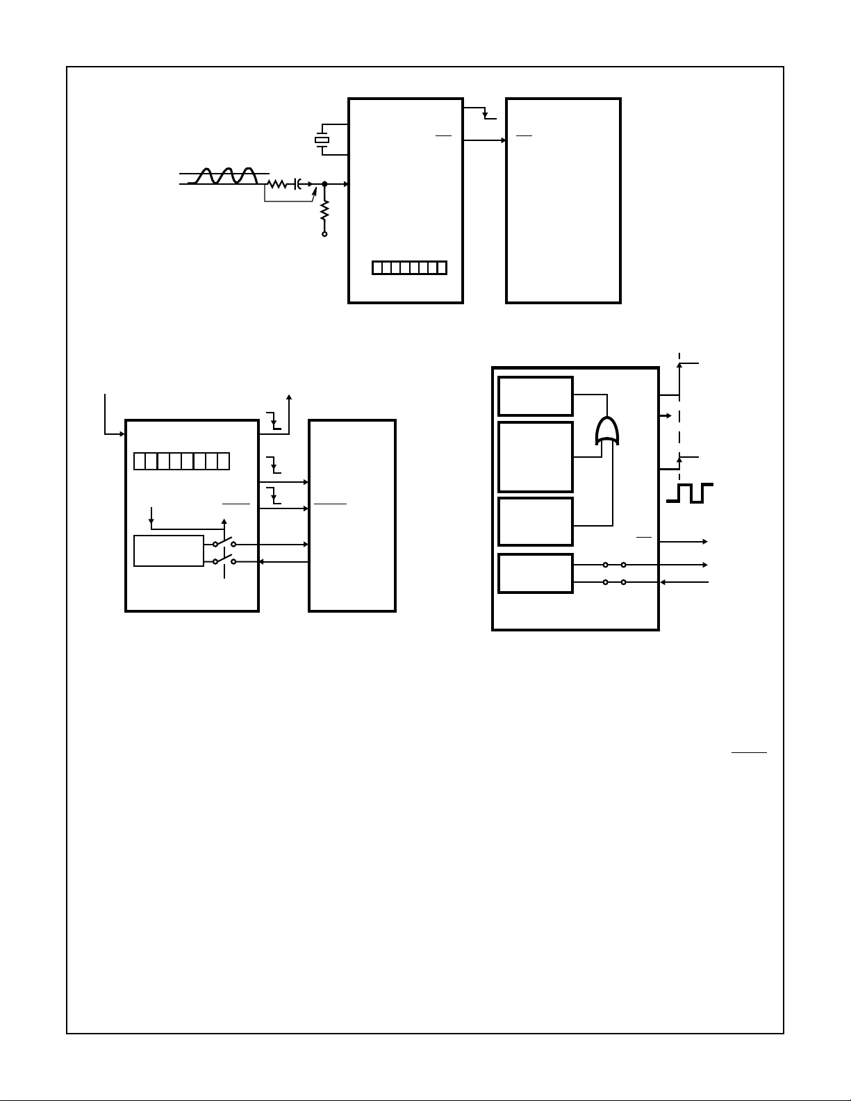
FIGURE 3. POWER-SENSING FUNCTIONAL DIAGRAM
FROM SYSTEM
POWER
V
SYS
I
INTERRUPT
CONTROL
REGISTER
SERIAL
INTERFACE
REAL-TIME CLOCK
CDP68HC68T1
TO SYSTEM
POWER CONTROL
PSE
CLK
OUT
CPUR
MISO
MOSI
OSC
RESET
CPU
CDP68HC05C4B
POWER
UP
POWER
SENSE
OR
ALARM
CIRCUIT
PERIODIC
INTERRUPT
SIGNAL
SERIAL
INTERFACE
REAL-TIME CLOCK
CDP68HC68T1
PSE
CPUR
CLK
OUT
INT
MISO
MOSI
FIGURE 4. POWER-DOWN FUNCTIONAL DIAGRAM FIGURE 5. POWER-UP FUNCTIONAL DIAGRAM (INITIA TED
BY INTERRUPT SIGNAL
Power Sensing (See Figure 3)
When Power Sensing is enabled (Bit 5 = 1 in Interrupt Control Register), AC transitions are sensed at the LINE input pin.
Threshold detectors determine when transitions cease. After
a delay of 2.68ms to 4.64ms, plus the external input circuit RC
time constant, an interrupt is generated and a bit is set in the
Status Register. This bit can then be sampled to see if system
power has turned back on. See PIN FUNCTIONS, LINE PIN.
The power-sense circuitry operates by sensing the lev el of the
voltage presented at the line input pin. This voltage is centered around V
threshold (about 1V) from V
and as long as it is either plus or minus a
DD
a power-sense failure will not
DD
be indicated. With an AC signal present, remaining in this
V
window longer than a minimum of 2.68ms will activate
DD
the power-sense circuit. The larger the amplitude of the AC
signal, the less time it spends in the V
likely a power failure will be detected. A 60Hz, 10V
window, and the less
DD
P-P
sinewave voltage is an applicable signal to present at the LINE
input pin to setup the power sense function.
Power Down (See Figure 4)
Power down is a processor-directed operation. A bit is set in
the Interrupt Control Register to initiate operation. 3 pins are
affected. The PSE (Power Supply Enable) output, normally
high, is placed low. The CLK OUT is placed low. The
CPUR
output, connected to the processors reset input is also
placed low. In addition, the Serial Interface is disabled.
Power Up (See Figure 5 and Figure 6)
Two conditions will terminate the Power-Down mode. The
first condition (See Figure 5) requires an interrupt. The interrupt can be generated by the alarm circuit, the programmable periodic interrupt signal, or the power sense circuit.
The second condition that releases Power Down occurs
when the level on the V
level at the V
V
(See Figure 6) in the Battery Backup Mode or V
BATT
input, after previously falling to the level of
BATT
pin rises about 0.7V above the
SYS
falls to logic low and returns high in the Single Supply Mode.
8
SYS
 Loading...