

CDP68HC68S1
April 1994
Features
• Differential Bus for Minimal EMl
• High Common Mode Noise Rejection
• Ideal for Twisted Pair Wiring
• Data Collision Detection
• Bus Arbitration
• Idle Detection
• Programmable Clock Divider
• Power-On Reset
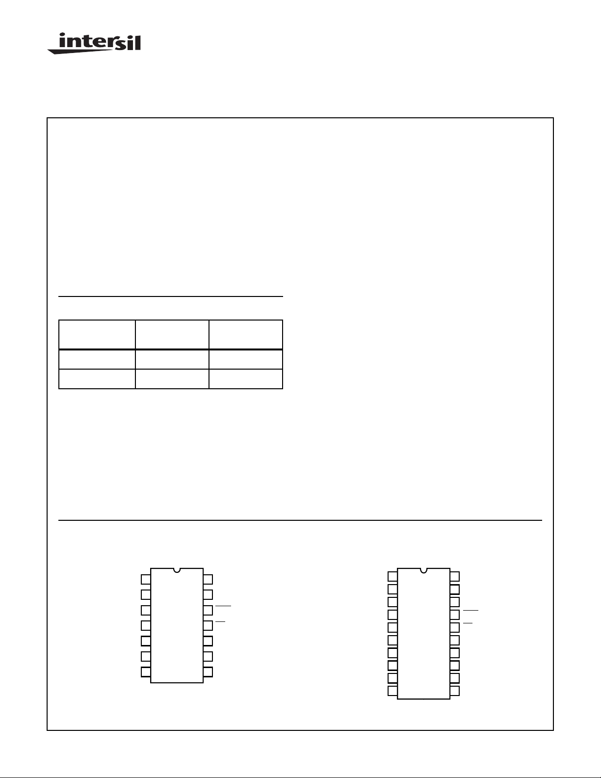
Ordering Information
PART
NUMBER
CDP68HC68S1E -40oC to +105oC 14 Lead PDIP
CDP68HC68S1M -40oC to +105oC 20 Lead SOIC (W)
TEMPERATURE
RANGE PACKAGE
Serial Multiplexed Bus Interface
Description
The CDP68HC6SS1 Serial Bus Interface Chip (SBlC) provides
a means of interfacing in a Small Area Network configuration,
various microcomputers (MCU’s) containing serial ports. Such
MCU’s include the family of 68HC05 microcontrollers. The SBlC
provides a connection from an MCU’s Serial Communication
Interface (asynchronous UART type interface) or Serial Peripheral Interface (synchronous) to a medium speed asynchronous
two wire differential signal bus designed to minimize electromagnetic interference. This two wire bus forms the network bus
to which all MCU’s are connected (through SBI chips). See Figure 1. Each MCU operates independently and may be added or
deleted from the bus with little or no impact on bus operation.
Such a bus is ideal for inter-microcomputer communication in
hazardous electrical environments such as automobiles, aircraft
or industrial control systems.
In addition to acting as bus arbitor and interface for microcomputer SCI port to differential bus communication, the
CDP68HC68S1 contains all the circuitry required to convert
and synchronize Non-Return-to-Zero (NRZ) 8-bit data received
on the differential bus and clock the data into a microcomputer’s
SPl port. Likewise, data to be sent by a microcomputer’s SPI
port is converted to asynchronous format by appending start
and stop bits before transmitting to other microcomputers.
Pinouts
CD68HC68S1 (PDIP)
TOP VIEW
CLK
1
2
A
3
B
4
MODE
5
BUS+
6
BUS-
7
V
SS
V
14
CONTROL
13
IDLE
12
CS
11
SCK
10
REC
9
8
XMIT
DD
Refer to the data sheet for the CDP68HCO5C4 for additional
information regarding CDP68HCO5 microcomputers and their
Serial Communications and Serial Peripheral Interfaces.
The CDP68HC68S1 is supplied in a 14 lead dual-in-line plastic
package (E suffix), and in a 20 lead small outline plastic package (M suffix).
Operating voltage ranges from 4V to 7V and operating temperature ranges from -40
o
C to +105oC.
CD68HC68S1 (SOIC)
TOP VIEW
1
CLK
A
2
B
3
MODE
4
NC
5
NC
6
BUS+
7
8
NC
9
BUS-
V
10
SS
V
20
CONTROL
19
NC
18
IDLE
17
CS
16
SCK
15
NC
14
NC
13
12
REC
11
XMIT
DD
CAUTION: These devices are sensitive to electrostatic discharge; follow proper IC Handling Procedures.
407-727-9207
| Copyright © Intersil Corporation 1999
6-84
File Number
1918.3
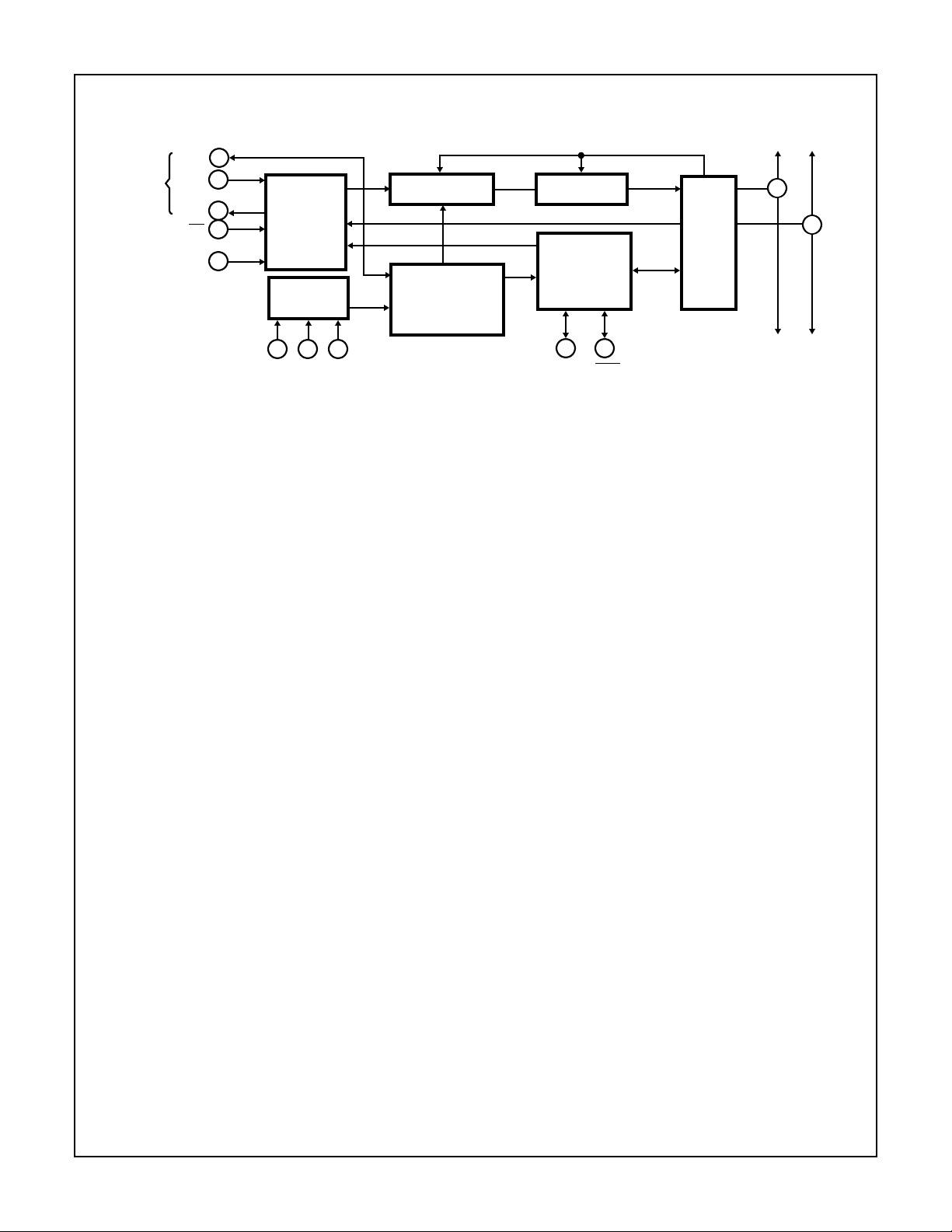
Block Diagram
CDP68HC68S1
TO
FROM
MCU
SCK
XMIT
REC
CS
MODE
SPI/SCI
CONVERSION
CLOCK
DIVIDER
CLK A B
ARBITRATION
DETECTOR
WORD COUNTER
AND
CLOCK
GENERATOR
COLLISION
DETECTOR
IDLE
DETECTION
AND
CONTROL
CONTROL IDLE
BUS+
BUS-
DIFFERNTIAL
DRIVER/RECEIVER
TO OTHER
SBI CHIPS
6-85
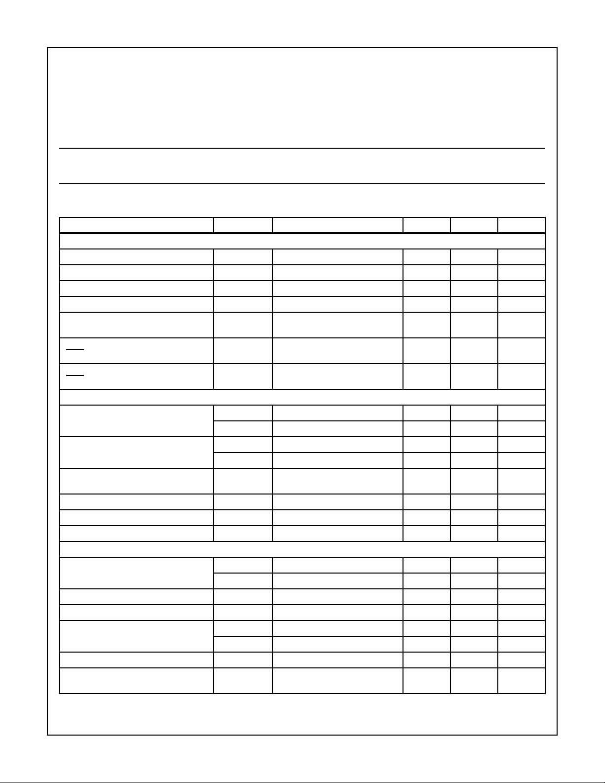
Specifications CDP68HC68S1
Absolute Maximum Ratings Thermal Information
Supply Voltage (VDD) . . . . . . . . . . . . . . . . . . . . . . . . . -0.3V to +7.0V
Input Voltage (VIN) . . . . . . . . . . . . . . . . . . VSS -0.3V to VDD+0.3V
DC Input Current (IIN) . . . . . . . . . . . . . . . . . . . . . . . . . . . . . . . . . .±10mA
CAUTION: Stresses above those listed in “Absolute Maximum Ratings” may cause permanent damage to the device. This is a stress only rating and operation
of the device at these or any other conditions above those indicated in the operational sections of this specification is not implied.
Operating Conditions
Operating Temperature (TA). . . . . . . . . . . . . . . . . . -40oC to +105oC DC Operating Voltage Range (VDD) . . . . . . . . . . . . . . . . +4V to +7V
Thermal Resistance θ
Plastic DIP Package. . . . . . . . . . . . . . . . . . . . . . . . . . . . 100oC/W
DC
Plastic SOIC Package . . . . . . . . . . . . . . . . . . . . . . . . . .120oC/W
Storage Temperature Range (T
) . . . . . . . . . . . .-55oC to +125oC
STG
Lead Temperature (Soldering 10s) . . . . . . . . . . . . . . . . . . . . +265oC
JA
DC Electrical Specifications T
= -40oC to +105oC Unless Otherwise Noted. External Bias (VO) shall be 1.8V to 3.13V Unless
A
Otherwise Noted.
PARAMETERS SYMBOLS TEST CONDITIONS MIN MAX UNITS
SIGNAL I/O SECTION
Output Voltage High Level V
Output Voltage Low Level V
Input Voltage Low Level V
Input Voltage High Level V
Output High Drive (Source) Current
OL
OH
IL
IH
I
OH
Open Circuit - 0.05 V
Open Circuit VDD-0.05 - V
- 0.3V
0.7V
DD
DD
-V
V
VOH = 4.6V, VDD = 5V -0.12 - mA
DC
DC
DC
DC
(REC Pin)
Output High Drive (Source) Current
I
OH
VOH = 4.6V, VDD = 5V -0.04 - mA
(IDLE, Control Pins)
Output Low Drive (Sink) Current
I
OL
VOH = 0.4V, VDD = 5V 0.36 - mA
(IDLE, Control, REC)
DIFFERENTIAL TRANSCEIVER (SEE FIGURE 4) TRANSMITTER
BUS+ I
BUS- I
I
- I
AOL
Match I
BOL
AOL
I
AOH
BOL
I
BOH
M
VO = VDD/2, RL = 120Ω 2.75 - mA
VO = VDD/2, RL = 120Ω -1.0 1.0 µA
VO = VDD/2, RL = 120Ω - -2.75 mA
VO = VDD/2, RL = 120Ω -1.0 1.0 µA
VO = VDD/2, RL = 120Ω,
-5%
VDD = 5V ±0.5V
Output Rise Time (BUS+) t
Output Fall Time (BUS-) t
Transition match (50% Point) t
R
F
M
VDD = 5V, CL = 25pF - 1.5 µs
VDD = 5V, CL = 25pF - 1.5 µs
VDD = 5V, CL = 25pF -50 50 ns
RECEIVER
Differential Sensitivity V
Hysteresis (Within V
IDH
, V
Limits) V
IDL
Propagation Delay t
Out of Range V
Quiescent Device Current I
Clock Speed f
IDH
V
IDL
H
P
AX
V
MIN
DD
OP
VO = 2.5V, RL = 120Ω, VDD = 5V - 120 mV
VO = 2.5V, RL = 120Ω, VDD = 5V 20 - mV
VO = 2.5V, RL = 120Ω, VDD = 5V 20 - mV
V
=120mV, VDD = 5V - 700 ns
IDH
VDD = 5V 3.8 - V
VDD = 5V - 1.2 V
VDD = 0V, VO = 2.5V -10 10 µA
VDD = 5, RL = 120Ω, CL = 25pF - TBD
MHz
(Note)
NOTE: Although 1MHz is generally used as an example throughout this datasheet, the maximum speed limit may be higher and depends
upon user’s noise tolerance requirements.
6-86
CDP68HC68S1
The Serial Bus IC offers the user three possible modes of
operation as defined by Table 1 - SCl (Note 1), SPl, and Buffered SPl. Also included is a “three-state mode” entered by
pulling the CS pin high while in the Buffered SPI mode. As
the name implies, the SCl mode is used when communicating through the microcomputer’s SCl port. In this mode,
asynchronous NRZ data format (1 start bit, 8 data bits ‘least
significant bit first’, and 1 stop bit) and baud rate remain the
same on each “side” of the SBlC, i.e. to and from the micro
and to and from the differential network bus.
TABLE 1. MODE AND CHIP SELECT DEFINITION
SBI CHIP MODE MODE PIN CS PIN
SCI 1 1
SPI 1 0
Buffered SPI 0 0
Three-State (Note 2) 0 1
NOTES:
1. SCI is the UART interface of a 68HCO5 MCU. The
CDP68HC68S1 is compatable with most UART devices.
2. The three-state mode is only entered when using the Buffered
SPI mode. In the three-state mode, only the XMIT, REC, and
SCK pins are three-stated. The CONTROL and IDLE pins are always active.
During data transmission, while a byte is being transmitted
from the MCU through the SBl chip onto the differential bus,
it is also reflected and simultaneously received back at the
micro, (this is required for bus arbitration as described later).
DIFFERENTIAL BUS
SBI SBISBI
bus “monitoring”. The Serial BUS Interface chip handles bus
arbitration, data collision detection, and provides short circuit
protection.
A 68HC0S MCU’s SPI port may instead be used for bus
communication. Two modes of SPl operation are available
with the SBIC - one essentially places the 68HC05 microcomputer in the slave mode and the other allows the MCU to
remain a master. In the normal SPl mode the SBIC acts as a
master and supplies a data-synchronizing serial clock signal
to the micro (which operates in the slave mode) for shifting
data in or out of the micro’s 8-bit SPl data register. Again,
baud rates are the same on each side of the SBlC, however,
the user must reverse the bit order of a byte transmitted or
received via the SPI port due to the SPl’s most significant bit
first serial data nature. In addition, since the user microcomputer is operating in the slave mode it must signal the SBI
chip (by pulling the CONTROL line low) to initiate a transmission. As in the SCl mode, during a transmission, the byte
originally in the SPI data register is replaced by the byte
reflected from the bus.
Transmission and reception of data in the Buffered SPI mode
allows the user to free the micro’s SPl port by allowing fast
data communication (1M bits/second) between the SPI port
and SBlC. For instance, if the MCU is transmitting, the SBlC
converts the data stream from the MCU’s SPl port to a
slower speed for transmission along the differential bus
when the bus becomes idle. Data speed conversion is
accomplished via a 2 byte (16-bit) data buffer register residing in the serial bus chip. In this mode the MCU operates as
a master and provides the serial clock signal to the slave
SBlC peripheral. After fast data has been sent to or received
from the SBIC, the micro can pull the SBlC’s
CS pin high
(placing the SBlC chip in the three-state mode) and then use
the SPl port to access other SPl peripherals.
All transfers between the user MCU and the SBlC in the
Buffered SPI mode consist of 2 bytes, i.e. a message consists an even number of 8-bit transfers. A microcomputer
wishing to transmit loads 2 bytes into the serial bus IC data
register and then pulls the control pin low to initiate transmission. During transmission the 2 bytes placed into the buffer
are replaced by the two reflected bytes received from the
bus. After every 2 byte transmission the user micro should
transfer the two reflected bytes out of the buffer and the next
2 bytes to be transmitted into the buffer.
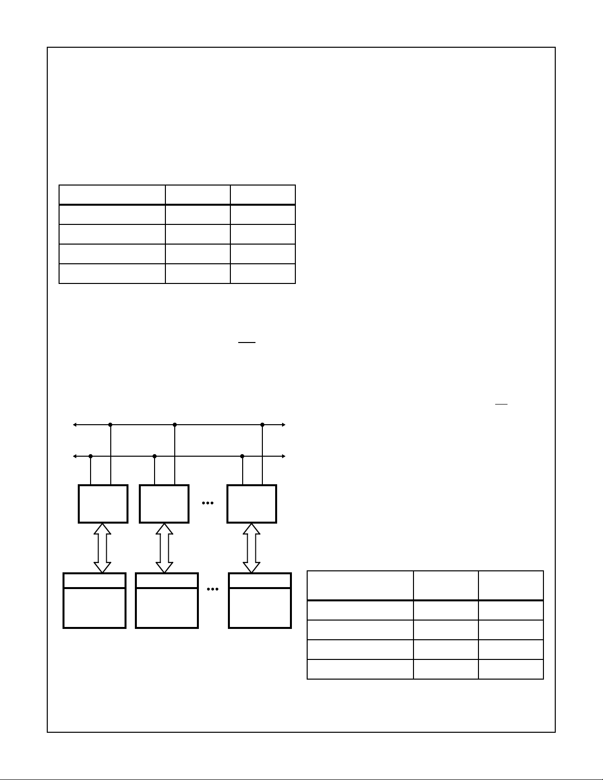
TABLE 2. CLOCK PROGRAMMING
SPI OR SCI SPI OR SCISPI OR SCI
MCU
FIGURE 1. POSSIBLE NETWORK CONFIGURATION-VARIOUS
MICROCOMPUTERS USING SBI CHIPS TO COMMUNICATE ALONG DIFFERENTIAL BUS.
MCU
MCU
In addition to performing a framing error check in the SCI
mode, other advantages gained by using the SBlC (in any
mode) include greater system EMl tolerance and automatic
CLOCK INPUT
DIVIDE FACTOR A PIN B PIN
÷ 100
÷ 201
÷ 410
÷ 10 1 1
6-87
CDP68HC68S1
Functional Pin Description
PIN NUMBER SYMBOL IN/OUT DESCRIPTION
1 CLK Input This is the clock input that shall be divided by the SBIC (as described in Table 2) and used
as an internal synchronizing clock. The internal clock is then further divided by 128 to determine baud rate, i.e. 128 internal clock periods constitute 1-bit length.
2, 3 A and B Input Programing inputs of the clock divider. These inputs are tied to +VDD or VSS depending
upon speed of external clock source. (See Table 2)
4 Mode Input This input shall be used in conjunction withCS input to define the mode of operation (see
Table 1). It may be permanently wired to +VDD or VSS or driven high or low by MCU I/O
lines.
5, 6 BUS+
and BUS-
14, 7 VDD and
V
SS
8 XMIT Input In the SCI mode this data input shall come from the microcomputer standard NRZ asyn-
9 REC Output In the SCI mode this data output shall be fed into the microcomputer asynchronous com-
10 SCK Input/Output In the SCI mode, this I/O is not required. In both SPI modes this pin is connected to the
11 CS Input This input shall be used in conjunction with the mode input and shall be used as a chip
12 IDLE Input/Output The microcomputer shall monitor this signal to determine the bus condition and also pull
Input/Output This is the two wire differential bus I/O used to transmit and receive data to and from the
differential bus. BUS+ is both responsive to, or driven positive by sourcing current from
an externally established bias point. This sourcing current matches the BUS- I/Os sinking
current. BUS- is both responsive to, or driven negative by sinking current from an externally established bias point. This sinking current matches the BUS+ I/Os sourcing current.
- Power and ground reference are supplied to the device via these pins. VDD is power and
VSS is ground.
chronous communications output port (68HC05 SCI port pin TxD). In the SPI modes, it
shall come from the microcomputer’s synchronous output port (68HC05 SPI port pin
MOSl or MlSO).
munications input port (68HC05 SCI port pin RxD). In the SPI modes it shall be fed into
the microcomputer’s synchronous input port (6805 SP1 port pin MOSl or MISO).
68HC05’s SPI port SCK pin. In the normal SPl mode, the SBlC shall produce shift clock
pulses via this pin for synchronously shifting data into and out of the microcomputer. In
the Buffered SPl mode this pin is an input and the microcomputer shall generate the shift
clock pulses. Figure 3 shows the relationship between the serial clock signal and other
SBIC signals in the SPI mode.
select (see Table 1). It may be permanently wired to +VDD or VSS or driven high or low by
MCU I/O lines.
this line low to generate a break. The IDLE signal goes low when the bus is idle (after
sensing an End of Message condition) and high when the bus is active. On reset, this pin
is set to a logic zero.
13 Control Input/Output The microcomputer shall monitor this I/O pin in the SPl mode to handle transmission and
reception of data. In the SCI and SPI modes, as an output, this pin will go low to indicate
that a data byte is currently active on the bus. In the Buffered SPI mode the control pin
indicates whether the user microcomputer has current access to the SBI chip’s internal 2
byte buffer (signified by a logic high on the control pin). In both SPI modes the control pin
is also effective as an input. In these modes the control pin is pulled low by the user microcomputer to initiate a transmit operation by the SBlC. The control pin is normally high
when the bus is inactive. On reset, this pin is set to a logic high.
All Intersil semiconductor products are manufactured, assembled and tested under ISO9000 quality systems certification.
Intersil products are sold by description only. Intersil Corporation reserves the right to make changes in circuit design and/or specifications at any time without
notice. Accordingly, the reader is cautioned to verify that data sheets are current before placing orders. Information furnished by Intersil is believed to be accurate
and reliable. However, no responsibility is assumed by Intersil or its subsidiaries for its use; nor for any infringements of patents or other rights of third parties which
may result from its use. No license is granted by implication or otherwise under any patent or patent rights of Intersil or its subsidiaries.
For information regarding Intersil Corporation and its products, see web site http://www.intersil.com
6-88

CDP68HC68S1
Differential Transceiver Cell
The differential transceiver is a serial interface device which
accepts digital signals and translates this information for
transmitting on the two wire differential bus.
The transmitter section (shown in Figure 4), when transmitting, provides matched constant current sources to the bus
“+” and bus “-” I/O sourcing and sinking respectively. When
transmitting, a logic zero at the “transmit data” input causes
the bus “+” I/O to provide source current and the bus “-” I/O
to provide a matched sink current. A logic one at the “transmit data” input causes the bus “+” and bus “-” I/Os to simultaneously provide a high impedance state. The bus depends
on external resistor components for bias and termination.
Recommended resistor sizes are shown in Figure 4.
SBI CHIP
TRANSMIT
DATA
----------------- -
BREAK
RECEIVE
DATA
OUTOF
RANGE
FIGURE 4. DIFFERENTIAL DRIVER/RECEIVER
A zero transmitted on the bus will appear as a large voltage
drop across the BUS+ and BUS- pins, i.e. BUS+ might typically sit at +2.8V and BUS- at +2.2V for a logic zero. For a
logic level one, the SBlC actually three-states the BUS+ and
BUS- pins and relies on external resistors to bias the bus
lines. The lines are both biased to sit at approximately 2.5V
with a small (perhaps 20mV) voltage drop across the two
lines. In this condition the BUS- line actually sits at a slightly
higher potential than the BUS+ line. See Figure 5. Thus, the
V
DD
I
A
+
-
BUS+
BUS-
I
B
V
C
L
CLC
DD
L
13KΩ
13KΩ
120Ω
DIFF.
BUS
DIFF.
BUS
bus actually “floats” to a logic level one, but must be driven to
a logic level zero. Logic 0-bits always dominate over logic 1bits on the bus. If two MCU’s simultaneously transmit a zero
and a one on the bus, the zero will override the one and the
bus will merely appear to be transmitting a zero. The “marking” or idle signal on the bus is a logic one. If the bus is idle
or if a micro is sending a logic one, then a one will appear on
the bus.
In addition to the transmission of data, the differential data
transceiver accepts at its bus “+” and bus “-” I/Os, serial differential data which is translated into the standard digital
logic levels. This reception of data also occurs while transmitting, thus reflecting the data seen on the bus back into the
SBIC data register.
VDD = 5V
2.8
2.5
2.2
20mV MAX.
BUS-
BUS+
LOGIC 0
0.6V
LOGIC 1
LOGIC 0
Typical voltage levels seen on BUS+ and BUS-
APPROX.
VOLTAGE
I/O pins for logic zero and logic 1-bits. Notice
that the BUS- Pin is biased to actually sit a
higher voltage potential than the BUS+. Values
shown are for VDD = 5V
FIGURE 5.
The differential transceiver cell allows bus activity by other
devices on the bus “+” and bus “-” I/Os when power to the
cell is shut off. Therefore, this powered off condition places
the transceiver outputs, BUS “+” and BUS “-”, in a high
impedance state. When the cell is either being powered up
or down, with or without bus activity, SCR latch-up protection
is provided such that this activity is not affected.
DIFFERENTIAL
CONTROL (1)(3)
BUS
SCK
XMIT
REC
CONTROL (2)
IDLE
START
BIT
01234567
12345678
654321
MSB
MSB
654321
LSB
LSB
STOP
BIT
(4)
IDLE IDLE
BIT BIT
IDLE
IDLE
IDLE
IDLE
IDLE
IDLE
IDLE
BIT
BIT
BIT
BIT
BIT
1234 567 891011
BIT
BIT
IDLE
BIT
NOTES:
1. The control signal at the transmitting node.
2. The control signal at the receiving node.
3. There is a delay between the control pin being pulled low and the actual beginning of the start bit.
4. If the control pin is again puled low before the end of the stop bit, then the next start bit will begin at the end of the previous stop bit.
FIGURE 3. SCK, CONTROL, AND IDLE SIGNALS DURING THE SPI MODE OF OPERATION
6-89
IDLE
BIT

CDP68HC68S1
Receive data is an output from the differential transceiver
cell. It is the output of a differential amplifier which decodes
the bus “+” and “-” I/O. When the bus “+” and “-” has been
driven positive and negative respectively to a differential voltage value greater than V
, the output of the differential
IDH
amplifier is a logic one, which is inverted and considered a 0bit from the bus. Otherwise, for level below V
the differen-
IDL
tial amplifier output is a logic zero, which, in turn, is inverted
and considered a 1-bit from the bus.
Twisted wire pair (or adjacent PC board traces) is recommended for the two differential bus lines.
The BREAK input, when held at a logic zero, (low) causes
the differential transmitter driver to generate a continuous
logic level zero on the differential bus. This action can generate a data collision which can be either used as a break or a
request for arbitration by the system. When held at logic one,
(high) this input has no effect on the operation of the cell.
The out of range output is normally a logic zero but goes to a
logic one when the common mode voltage on both differential bus inputs exceeds a voltage value greater than V
less than V
(see device specifications). This output is
MIN
MAX
or
used by a latch to hold the received data at the logic level it
was before the over range signal occurred.
Provided on chip is a power-on reset function. The transceiver
cell’s reset output is held to a logic zero on power up and
switches to a logic one at or before V
rises to 4.0V . This out-
DD
put is used to ensure that other on-board logic has been properly initiated. During this reset time, the bus “+” and the bus “-”
l/Os provide a high impedance state to the bus.
Bus Speed
SBlC systems typically use a bus speed of 7812.5 bits/second which is accomplished by using a 1MHz internal clock.
However, no restriction on any other baud rate is designed
into the chip, except its upper speed limit (see device specifications).
Bus Byte Format
All bytes transmitted on the bus follow the standard UART
style asynchronous non-return-to zero data format consisting oft start bit (logical zero) followed by 8 data bits (LSB
first), and 1 stop bit (logical one).
Bus Message Format
All messages transmitted on the bus consist of a number of
bytes, from 1 to N, with no restriction on length. The user must
be aware, however, that the longer the message length, the
greater the probability of collision with messages being transmitted at random from other masters on the bus. Typical message lengths of systems now in use range from 1 to 4 bytes.
The actual definition of each byte sent is left for the user to
determine, i.e. the user must define the system protocol. For
instance, a typical (and recommended) protocol might dictate that the first byte of each message sent be a unique
address/identification byte. The first byte sent by a node (an
MCU coupled with an SBl chip) might contain address information telling where (to which node[s]) the message is targeted for or where the message came from.
Other possibilities would be to identify the type of message
sent (e.g. an instruction or just information) or the length of
the message. The remaining bytes in each message can be
merely data bytes that comprise the actual message. The
user can even use the last byte as a check sum so that all
receiving nodes can check for errors in transmission.
Messages are normally received by all nodes on the bus and
may be processed by one or more micros, i.e., each MCU
may decide, after receiving the first byte (address/ID byte)
that this particular message is not needed for its operation.
The MCU can then ignore the remainder of the message.
Prioritization
Since simultaneous transmission of address/ID bytes from
several microcomputers is a possibility, a system of prioritization should be determined for bus arbitration. Due to the
electrical characteristics of the differential data bus, each
unique address/ID byte can automatically contain priority
information used for bus arbitration. Merely use “lower” value
ID bytes for higher priority messages. “Lower” value, in the
SBlC case, means an ID byte with more zero’s in its least
significant locations. To further explain, since the differential
bus transmits data least significant bit first and a zero overrides a 1-bit simultaneously transmitted by different nodes,
an ID byte with least significant bit equal to zero will override
an ID byte from a micro whose least significant bit is a one. If
this does occur on-chip bus arbitration will automatically
allow only one SBlC chip (with the highest priority address/
ID byte) to continue transmitting. In this case it is the micro
who transmitted the 0-bit. Assuming both ID bytes contain
identical LSBs (bit 0) then arbitration is carried on to the next
bit (bit 1),and soon.
Reflected Data
Whenever a microcomputer sends data through the SBIC
and onto the differential bus, it will always receive reflected
data back. The reflected data is the data that was actually
seen on the bus. Keep in mind that during data collisions
between simultaneously transmitting micros, zeroes override
ones. In addition, any noise that may have been induced on
the bus may alter the resultant reflected byte.
Bus Arbitration
Bus arbitration is the attempted transmission onto the differential bus of an initial byte (preferably an address/ID byte) by
one or more user microcomputers. The purpose of bus arbitration is to enable a single microcomputer to obtain sole
usage of the bus for the purpose of transmitting a message.
Bus arbitration is accomplished via a combination of methods which include an MCU software comparison of transmitted bytes to reflected bytes, the SBlC’s collision detection
circuit, and its start bit arbitration detector circuits.
Collision Detection
The SBlC’s collision detector circuit compares the bits being
sent from a user microcomputer to the reflected byte simultaneously received back from the differential bus. If the collision detector detects a difference in the data, it immediately
blocks the user microcomputer’s transmitted data from fur-
6-90

CDP68HC68S1
ther reaching the bus. This will happen, as stated in the “Prioritization” section, when a micro with a higher priority
address/ID byte attempts “simultaneous” transmission (actually, i.e. within a time window of 1/4 bit time).That micro, with
a higher priority ID byte, is obviously sending a 0-bit and its
reflected byte matches the byte it is sending. Not detecting a
collision, it continues to transmit its message, while the lower
priority MCU is cut off from transmitting on the bus. The
lower priority micro will be inhibited from transmitting on the
bus until the message presently on the bus has ended
(EOM = “End of Message” condition).
End of Message Condition
After transmitting the last byte of a message, the transmitting
MCU must generate an End of Message (EOM) condition.
An EOM condition is defined as a 10-bit length idle condition, i.e., the bus must remain idle (logic1) for a period of 10bit times (1280 internal clock periods). This can be done by
merely creating a 10-bit delay in MCU software.
Start Bit Arbitration Detection
Arbitration, as discussed above, is only necessary when two
or more micros attempt to transmit within 1/4 bit time (32
internal clock periods) of each other. Otherwise, once a
micro begins a transmission on the differential data bus, all
other SBl chips sense the start bit and inhibit their microcomputers from transmitting (again, after a 32 clock period arbitration window delay). Once the arbitration detector circuit
has blocked an MCU’s transmission, access to the bus will
be blocked until an End of Message condition.
Start of Message Delay
In order to properly synchronize various MCU’s (which may
be using different modes of operation) for impartial arbitration, each node must delay 2-bit times (256 internal clock
periods) after detecting the
IDLE signal drop low before
transmitting, i.e., before the start bit of the next message
reaches the bus. When using the SPI or Buffered SPl
modes, this delay is automatically designed into the SBl
chip. However, when using the SCl mode, the MCU must
support this required delay. Fortunately, 68HC05 microcomputers using the SCI port will inherently experience a delay
between the time that the SCl data register is loaded and the
time that the start bit actually appears on the SCl port transmit pin (TxD). At a baud rate of 7812.5 bps this delay can be
as long as 256 SBl chip internal clock periods. If this is so,
then the user MCU does not have to worry about providing
this delay.
USER #1
XMIT #1
REC#1
USER#2
XMIT #2
REC #2
USER #3
XMIT #3
REC #3
DIFFERENTIAL
ALL CONTROL
ALL IDLE
BUS
PINS
PINS
ID BYTE FOR A MESSAGE
START
BIT
01234567
00010100
00010100
00100010
(2)
00010100
01000000
(3)
00010100
00010100
(6) (7)
NOTES:
1. USER #1 is note transmitting + marking.
2. Point at which USER #2 loses bus arbitration.
3. Point at which USER #3 loses bus arbitration.
4. Point at which USER #3 loses bus arbitration.
5. This ‘1’ bit is not overridden by the ‘0’ bits from users 2 and 3 because both users 2 and 3 have previously been blocked from bus access due to data collisions.
6. The control pin on the transmitting node goes low earlier in both SPI modes (it is pulled low by micro).
7. The control pin remains low until the end of the last data bit of the 2 byte set when using the buffered
SPI mode, but goes high at the middle of the last data bit in other modes.
(5)
STOP
BIT
10 IDLE BITS
ID BYTE FOR A DIFFERENT MESSAGE
START
BIT
01234567
(1)
00100010
00100010
00100010
01000010
(4)
00100010
(6) (7)
STOP
BIT
10 IDLE BITS
FIGURE 6. EXAMPLE OF THE SCI CHIP OPERATING DURING BUS ARBITRATION
6-91

Idle Detection
CDP68HC68S1
An idle detector circuit is used to detect when the differential bus
is in the idle condition, i.e., no user microcomputer has control of
the bus and the bus is sitting at a mark condition (a logic one).
The idle detector senses a received stop bit and delays for a
short idle period of 10-bit times, during which the bus must
remain idle. The idle output pin is then set to a logic zero (true). It
is later set to a logic one by receiving a start bit. During the 10-bit
time delay, if a non-idle condition such as noise is detected on the
bus, the delay period counter will be restarted.
Due to the 10-bit time idle delay period, once an MCU wins
bus arbitration, it should send the next data byte to be transmitted within a period of 10-bit times (1280 internal clock
periods). Each subsequent data byte to be sent should also
not exceed the interbyte maximum of 10-bit times. If this
maximum is exceeded, all SBlC chips will have detected the
idle condition and now pull their idle lines low and reset their
bus arbitration and collision detection circuits, thereby allowing other SBl chips with messages to send to arbitrate for the
bus. Figure 6 shows the detailed operation of the serial bus
interface chip during bus arbitration. This example shows the
arbitration of a single byte (e.g. the address/ID byte) from
three different user microcomputers. Two full arbitration
cycles are shown.
Break Generator
A request for arbitration can be generated by a node that
needs to interrupt transmission of a long data string. This
can be accomplished by forcing the SBlC’s
IDLE pin to a
logic zero; this forces a data collision (by sending 0-bits)
after three data bytes have been transmitted, and the transmitting MCU is required to detect this break condition and
stop transmitting. It is, however, allowed to re-arbitrate for the
bus and the interrupting mode may not generate a second
break condition if it loses arbitration.
Using the CDP68HC68S1
13KΩ
BUS-
MCU
SPI OR SCI
NOTE: Hardware configuration for a network consisting of two
microcomputers. Notice that the pullup resistor is connected to
the BUS- pin and the pulldown to BUS+.
13KΩ
120Ω 13KΩ
+V
DD
BUS- BUS+
SBIC SBICSBIC
SPI OR SCI
MCU
NOTE: Hardware configuration for a network consisting of 3 or
more MCU’s. Notice that the bus utilizes no more than 1 set of 13K
bias resistors and no more than two 120Ω termination resistors.
FIGURE 7. HARDWARE CONFIGURATION FOR A NETWORK
OF MICROCOMPUTERS
SBIC
BUS+
FIGURE 7A.
120Ω
BUS- BUS+ BUS- BUS+ BUS- BUS+
SPI OR SCI
MCU
FIGURE 7B.
120Ω
13KΩ
BUSSBIC
BUS+
SPI OR SCI
MCU
MCU
SPI OR SCI
SBIC
SPI OR SCI
MCU
Following are some hardware and software recommendations for using CDP68HC68S1 Serial Bus Interface Chip.
Requirements may vary depending upon the user’s system
configuration.
Hardware (General)
The differential bus lines (BUS+ and BUS-) must be terminated with external resistors as shown in Figure 4. This
applies, however, only to one node (an MCU/SBlC pair)
along the bus. Since all SBl chips are wired in parallel across
the network bus, there is no need for additional 13K bias
resistors at each node. The 120Ω termination resistors
should, however, be present at two nodes if the network
does indeed contain two or more nodes. The 120Ω resistor
provides the voltage drop across which the SBl chip senses
logic zero and logic 1-bits. If two nodes each utilize 120Ω termination resistors as shown in Figure 7A, the effective resistance across the BUS+ and BUS- pins drop to 60Ω total (due
to the parallel wiring method). Any less resistance would not
provide an ample voltage drop for the receiver cell op amp to
sense. Following these guidelines, typical systems might
look like those shown in Figure 7.
Software (General)
Although each user’s protocol may vary, the following general procedure should be followed when using the SBl chip
in any mode:
When a microcomputer is preparing to transmit a message it
should monitor the SBlC’s
(logic zero) indicating the bus is idle. Then the MCU
attempts to transmit the first byte (preferably an Address/ID
byte). If no other MCUs are transmitting at this time, or if this
MCU has the highest priority ID byte, the SBI chip’s collision
detector circuit will permit transmission.
The microcomputer must then confirm transmission by reading the byte reflected back from the bus. If this byte matches
the byte transmitted then the MCU has gained control of the
bus and may continue to transmit the remainder of the message (if any).
If the reflected byte does not match the ID byte sent then the
MCU has not gained control of the bus and may not presently transmit. It should, however, check the reflected ID
byte to see if the incoming message (i.e. the message from
6-92
IDLE pin and wait for it to go low

(START)
CDP68HC68S1
ANY MESSAGES TO TRANSMIT?
YES = ATTEMPT TO WIN BUS
ARBITRATION
TRANSMIT THE MSG ID BYTE.
NO
HAS THE MSG ID BEEN
RECEIVED FROM THE BUS?
DOES THE REC’D MSG ID EQUAL
THE TRANSMITTED MSG ID?
ARE THERE ANY MORE
MESSAGE BYTES TO TRANSMIT?
TRANSMIT THE NEXT MSG
ID BYTE.
YES
NO NO
YES
NO = LOST
YES = WON BUS ARB.
NO NO
YES = SEND REST OF MESSAGE
IDLE LOW?
IS
NO
ANY MSG ID RECEIVED?
YES = REC. A MSG
IS THIS MESSAGE OF
INTEREST TO US?
YES
SAVE THE RECEIVED BYTE.
HAS THE NEXT BYTE
BEEN RECEIVED YET?
NO
IS IDLE LOW?
YES
PROCESS THE MESSAGE.
NO
YES
HAS THE BYTE BEEN
REC’D FROM THE BUS?
YES
DOES THE REC’D BYTE EQUAL
THE TRANSMITTED BYTE?
YES
NO
NO
FIGURE 8. GENERAL MESSAGE PROCESSING.
the arbitration-winning MCU) is of any interest. If so, it
should save the incoming message (the length of which may
be specified in the ID byte) and then wait for the
IDLE line to
go high before re-attempting transmission (if still desired).
The flowchart in Figure 8 reflects this procedure.
The SCl Mode, Hardware
In the SCl mode, the TxD and RxD pins on the user microcomputer must be connected to the XMlT and REC pins on
the SBlC chip, respectively, as shown in Figure 9. The
MCU’s SCl port should be configured for the same baud rate
and character format as that used by the bus interface (i.e. 1
start bit, 8 data bits and 1 stop bit). The start and stop bits
are used to synchronize the data, a byte transfers between
the user microcomputer and the SBl chip. When using the
SCl mode, the SBl chip should always be properly mode and
chip selected. This can be accomplished by either a user
microcomputer output signal or by permanent wiring. This is
“TRANSMIT” AN END OF MESSAGE CONDITION.
ABORT THIS MESSAGE
TRANSMISSION
DUE TO A COLLISION.
required in order to always be able to receive messages
from other microcomputers on the bus, which can happen at
random. For the SCl mode, the SBl chip’s MODE pin must
be set to1 and the
CS pin to 1.
SCI Mode, Software
The procedure to follow for transmitting/receiving in the SCI
mode is basically identical to that stated in the “Using the
CDP68HC68S1-Software” section above, with the following
exception:
Start of Message Delay
Transmitting a byte via the 68HC05 SCl port basically requires
loading the byte into the MCU’s SCl data register (once the SCI
port is initialized). However, after the SBlC’s
low, the user may have to create a delay before transmitting the
FIRST byte of a message; this necessary 2-bit time (256 internal clock periods) delay is called the Start of Message (SOM)
IDLE pin drops
6-93

CDP68HC68S1
delay. Fortunately, SCl ports exhibit an inherent delay between
the loading of the transmit data buffer and the actual beginning
of the start bit appearing on the TXD pin. This delay, at 7812.5
Baud, can be as long as 256 SBl chip internal clock periods
and can be used to synchronize SCl users with SPI and Buffered SPI users to ensure impartial bus arbitration. The delay for
a particular microcomputer must be determined by the user. If
this inherent delay is less than 256 clock periods, then the user
must delay the loading of the first byte enough to ensure that
the total delay including the inherent delay of the SCl port is 256
clock periods.
MCU
TxD
RxD
PA
O
+V
FIGURE 9. USING THE SCI MODE
SBIC
XMIT
REC
IDLE
MODE CS
DD
BUS+
BUS-
DIFFERENTIAL
BUS
Monitoring the IDLE Pin
The user microcomputer must monitor the
IDLE pin on the SBlC
chip in order to determine when a message ends, when the next
received byte is a Msg ID byte, and when to attempt arbitration
if the user microcomputer has a message to transmit.
Framing Errors
While in the SCl mode, the SBI chip is capable of detecting
incoming framing errors. It will do this even though the
incoming signal is also echoed to the user microcomputer,
which should also detect the framing error via its’ UART.
When a framing error is detected by the SBl chip, the generation of the SCK pulses is terminated until and End Of Message is detected.
The SPI Mode Hardware
The Master Out Slave In, (MOSl), and Master In Slave Out,
(MISO), pins on the user microcomputer are connected to
the REC and XMlT pins of the SBl chip, respectively, as
shown in Figure 10. The SCK pins on the user microcomputer and the SBl chip are connected together. Synchronization of data transferred between the user microcomputer and
the SBl chip is done by using the SCK signal provided by the
SBl chip.
In the SPl mode of operation the SBl chip should always be
properly mode selected. This may be accomplished either
by a user microcomputer output signal or by permanent wiring in order to guarantee that the SBl chip will always be
able to receive messages from other microcomputers on the
bus, which may happen at random. To select the SPl mode,
set the MODE pin to a logic l and the
CS pin to a logic 0.
The user microcomputer must be able to both detect when
the
IDLE signal goes from high to low and sense at other
times whether it is either high or low. Detecting the change
from high to low is necessary in order to know exactly when
the bus goes idle. An MCU can then begin bus arbitration by
attempting to transmit. Being able to sense the level of
IDLE
is necessary in order to be able to start transmitting a message sometime after
IDLE has gone low but no other user on
the bus has had a message to transmit for a length of time.
Instead of polling the
IDLE pin via an MCU input pin, the
user may wish to conserve CPU time by using interrupts to
monitor bus activity. The user microcomputer’s external
interrupt pin (IRQ) can be used to edge detect the
IDLE pin
for high to low transitions.
Using 68HC05 SCl Port Flags
During message reception, the 68HC05 SCl port receive
data register full flag (RDRF), and optionally its associated
interrupt, can be used by the user microcomputer to determine when to unload the next received byte.
The user may wish to ignore the RDRF flag and disable the
RDRF interrupt during reception of an unwanted message.
In this case the user can merely wait for the
IDLE pin to go
low before attempting any further actions.
The normally available transmit data register empty flag
(TDRE) can be used to determine when to load the next byte
to be transmitted onto the bus. If there are no more bytes to
be transmitted, then consider the last message as having
been transmitted, and generate an End Of Message (EOM)
(i.e. transmit a logic 1 for 10 contiguous bit times by creating
a software delay).
MCU
MISO
MOSI
SCK
SS
PA
PA
FIGURE 10. USING THE SPI MODE
V
O
1
SS
+V
SBIC
XMIT
REC
SCK
IDLE
CONTROL
MODE CS
DD
BUS+
BUS-
DIFFERENTIAL
BUS
V
SS
The user microcomputer should configure its SPl port for
slave mode operation with SCK positive polarity and data
transfer on SCK leading edge (i.e. CPOL = 0, CPHA = 1, for
68HC05 microcomputers). 8-bit data transfers between the
user microcomputer and the SBl chip occur at differential
bus transfer speed.
In the SPI mode, the user microcomputer operates in the
slave mode and the SBl chip operates as the master. The
SS pin on the user microcomputer must be wired low or
forced low whenever the SBl chip has incoming data. It may
be useful to connect the CONTROL pin of the SBl chip to the
Slave Select (
SS) pin of the 68HC05 microcomputer. The
SBl chip will then control the user microcomputer’s SPI port.
The user microcomputer can request transmission of data
onto the bus by the SBl chip by loading data into its SPl data
register and then pulling the SBlC’s CONTROL pin low (for
at least 1µs). However, it must do so before the SBl chip has
begun to receive data from another MCU.
6-94

CDP68HC68S1
SPI Mode, Software
The SPl mode is similar to SCl mode in that the user microcomputer sends/receives data to/from the SBl chip 1 byte at
a time. In the SPI mode, however, the user microcomputer
must reverse the bit order of transmitted and received bytes.
When transmitting a message, each bit of a transmitted byte
is simultaneously transmitted onto the bus and a reflected bit
is simultaneously received from the bus.
Monitor and Control of the CONTROL Line
In the SPl mode, the user microcomputer monitors the CONTROL pin on the SBl chip in order to determine if the SBlC is
ready to accept a transmit request. Actually, a data collision
may still occur and the user microcomputer must always be
ready to handle it.
The CONTROL signal is normally high and goes low when
data is on the bus or when pulled low by the user microcomputer. After being pulled low by the user microcomputer , which
signals a request to begin the transmission data, the CONTROL signal will latch low and stay low until the middle of the
last data bit has been transmitted and appears on the bus.
The CONTROL signal will also go low at the beginning of the
first data bit, when received from the bus. It will then go high
at the middle of the last data bit.
When the SBl chip begins to receive a byte of data from the
bus and the user microcomputer has not pulled the SBlC’s
CONTROL line low, the SBl chip will pull CONTROL low and
start generating the SCK clock signal. As each data bit is
received it is clocked out of the SBl chip and into the user
microcomputer. Any data in the user microcomputer’s SPl
data register will be transferred out and into the SBl chip.
The CONTROL signal will go high at the midpoint of the
eighth data bit. This will allow the user microcomputer to
have enough time to review the just received SPl data and
reload it, if further data is needed to be transmitted. However, it must again pull the CONTROL pin low to signal he
SBl chip that it should begin transmitting. As a slave to he
SBl chip, the user microcomputer must be able to and le the
incoming data on the SPl port without affecting its other software routine functions.
Detecting
Interrupt
The user microprocessor’s external interrupt should be set
to edge detect
tion. If possible, detect CONTROL for rising transitions, for
byte transmission/reception complete detection.
Use of Internal User Microcomputer Flags and Interrupts
The normally available SPl finished flag (SPlF) and optionally
its associated interrupt may be used by the user microcomputer
to know when a byte transmission/reception of is complete.
The user microcomputer should be ready to handle the Write
Collision, WCOL, error flag. The WCOL flag is set when a
collision is detected in the SPl port. This will occur when the
user microcomputer tries to load a byte into the SPI data
register after the SBl chip has already begun to load data
into the SPl port.
IDLE via a User Microcomputer External
IDLE for falling transitions, i.e. EOM detec-
Sending Messages to Other Microcomputers on the Bus
ln order to send a message to other microcomputers on the
bus while in the SPI mode the user microcomputer should:
1. Monitor the
busy or if a transmission may be immediately started.
2. Monitor CONTROL to determine if it is ok to load the byte
to be transmitted into the user microcomputer’s SPl data
register.
3. Load the byte to be transmitted into the SPl data register.
4. Pull the CONTROL pin low to signal the SBl chip to start
a byte transmit cycle.
5. Wait until the byte transmit cycle is completed as signaled
by the SPl Finished, SPlF, flag/interrupt in the SPl port or
by the CONTROL signal going high.
6. Compare the received byte with the last transmitted byte.
7. If the received byte equals the last transmitted byte, and
more bytes remain to be transmitted, then continue the
cycle with step #3. If there are more messages to transmit, then go to step #1. If there are no more bytes to be
transmitted, then consider the message as having been
transmitted, and generate an End Of Message (EOM)
(i.e. delay for 10 contiguous bit times). Go to step #1.
8. If the received byte does not equal the last transmitted
byte and this is the first byte of a message, then treat the
received byte as the first byte of a received message (i.e.
the ID byte). Attempt to retransmit the previous message
after the
during the transmission of a later message byte, other
than the ID byte, then consider it due to either an erroneous data collision on the bus or due to noise collisions on
the bus causing the message to have to be re-transmitted. Go to step #1.
Framing Errors
While in the SPl mode, the SBl chip is capable of detecting
incoming framing errors. If one is detected, generation of the
SCK pulses to the user microcomputer is terminated. The
SBl chip essentially quits receiving data and starts looking
for an End Of Message. Resetting of the SCK generator will
occur upon receiving an EOM. Meanwhile, software must be
prepared to resynchronize the micro’s SPl port; this can be
done by disabling and then reinitializing it.
Even though the SBl chip can detect framing errors, it can
not flag the user microcomputer that one has occurred.
Since the previously received byte has already been transferred to the user microcomputer, the SBI chip will simply
refuse to accept any further incoming data until an EOM
occurs. Thus, one way that the user microcomputer may
detect that the received data is valid, is via using a check
sum byte imbedded within each message. Another way
would be to compare the number of bytes received fora particular ID to the number expected for that ID.
IDLE pin and determine if the bus is currently
IDLE signal has gone low again. If this happens
Buffered SPI Mode, Hardware
The MOSl and MlSO pins on the user microcomputer should
be connected to the XMlT and REC pins of the SBl chip
respectively. The SCK pins on the user microcomputer and
6-95

CDP68HC68S1
the SBl chip should also be connected together, as shown in
Figure 11. Synchronization of the data that is transferred
between the user microcomputer and the SBl chip is done by
the SCK signal which is provided by the user microcomputer.
The Slave Select (
SS) pin on the user microcomputer must
be wired high or forced high whenever the SBl chip is
selected.
The user microcomputer should configure its SPl port for
master mode operation, SCK low polarity, and data transfer
on first edge (i.e. CPOL = 0, CPHA = 1 for 68HC05 microcomputers).
The SBI chip must be chip selected either by a user microcomputer output signal or by permanent wiring of its pins. To
select the Buffered SPl mode, set the MODE pin and the
CS
pin to logic zero. This is required in order to transfer data
between the SBl chip and the user microcomputer. However,
in the Buffered SPl mode, since the MCU is operating as a
master and controls the SPI port, chip selection is only
required during when the SPl transfers are actually occurring.
MCU
MOSI
MISO
SCK
SS
PA
PA
FIGURE 11. USING THE BUFFERED SPI MODE
+V
O
1
DD
XMIT
REC
SCK
IDLE
CONTROL
MODE
+V
DD
SBIC
BUS+
BUS-
CS
DIFFERENTIAL
BUS
Buffered SPI Mode, Software
The principle difference between the Buffered SPI mode and
the normal SPl mode is the use of a 2 byte internal buffer.
Also, the Buffered SPl mode allows the user microcomputer
to operate in the master mode, instead of the slave mode,
which allows high speed transferring of data between the
SBl chip’s buffer and the user microcomputer.
For typical operation, the user microcomputer loads the
SBl’s 2 byte buffer, at a high speed, using its SPl interface.
The 68HC05’s SPl Finished flag (SPlF), and optionally its
associated interrupt, may be used by the user microcomputer to know when the transfer of a byte between the user
microcomputer and the SBl chip is complete. Then it signals
the SBl chip, by pulling its CONTROL line low, to transmit the
data in the buffer onto the differential bus.
The SBl chip, at a differential bus speed, then attempts to
transmit the buffered data onto the bus. During this attempt,
the SBl chip will receive two reflected bytes of data back
from the bus, store them in the buffer and then disable the
buffer from receiving further data from the differential bus
until this received data is later unloaded by the user microcomputer at high SPl transfer speeds. The MCU should also,
at this time, simultaneously load the next 2 bytes of data to
be transmitted into the buffer.
While it is transmitting and receiving the 2 bytes of data on
the differential bus the SBl chip will not allow transfer of data
to and from the user microcomputer. In fact, the SBl chip
does not need to be chip selected during this time.
The bus will override the user microcomputer if incoming
data is received during the time when the user microcomputer is performing a data transfer, after having unloaded the
previous 2 bytes. The data from the differential bus will be
loaded into the SBlC buffer, while the data from the user
microcomputer will be lost. The data that the user microcomputer will receive during this transfer, is undefined. The user
microcomputer has no way of knowing its transfer has been
aborted unless it either monitors the CONTROL signal for a
rising transition or by detecting that CONTROL was not high
at completion of the SPl transfer.
Monitoring the Control Signal
The user microcomputer should monitor the CONTROL signal on the SBl chip, in order to determine whether it is
actively transmitting or receiving data. The CONTROL signal
is used to determine who has access to the 2 byte buffer. During data reception or transmission to the differential bus by the
SBlC its CONTROL pin is low signifying that the differential
bus now has access to the SBlC and the MCU is locked out
from accessing the SBlC. Then when 2 bytes of data have
been received from the differential bus, the SBl chip will pull its
CONTROL line high, signaling to the MCU that the MCU can
now access the SBlC’s 2 byte buffer . The MCU may now read
the 2 bytes received and simultaneously transmit two more
bytes (if desired) by performing a 2 byte transfer (a swap of
data), via the MCU SPl port, with the SBlC; then the MCU
pulls the SBlC’s CONTROL pin low to transmit the two new
bytes. The CONTROL pin will remain latched low (by the
SBlC) until the two new bytes are transmitted.
The user microcomputer should also monitor the
IDLE signal
in order to accurately know when the bus is idle or when bus
arbitration is occurring, when a received message has finished,
and when the next bytes to be received are the beginning bytes
of a new message. Preferably, the user microcomputer’s external interrupt should be set up to edge detect falling
IDLE and
rising CONTROL transitions.
When the CONTROL pin goes high, it signals that the buffer is
full and that the user microcomputer currently has access. When
the
IDLE pin goes low, it is signaling that the current message
has been completed, and an MCU may now arbitrate for the bus.
Size of Messages that can be Transmitted or Received
In the Buffered SPI mode, the user microcomputer can only
send messages in 2 byte multiples. Transmitting messages
with an odd number of bytes, to other microcomputers on the
bus, is NOT supported by the SBl chip in Buffered SPl mode.
However, reception of any number of bytes is supported.
In the Buffered SPl mode, the user microcomputer can receive
messages of any length. For odd length messages, the user
microcomputer must know when the message is finished either
from the message ID byte or via the
IDLE signal. Since the SBl
chip will give no indication as to whether the buffer contains one
or 2 bytes of information from the bus, the message length
should be contained within the message data bytes.
6-96

CDP68HC68S1
When a single byte is received from the bus, followed by a
bus idle condition, the SBl chip will, as it normally does when
the buffer has received 2 bytes, set the CONTROL signal
high. It will then relinquish control of the buffer for data transferral via the user microcomputer, and restrict access to the
buffer from incoming bus data until the 2 byte data transfer
has been completed.
If only 1 byte is received from the bus, the user microcomputer will receive it first when performing the 2 byte data
transfer. The second byte received by the user microcomputer, during this transfer, is undefined. A 2 byte transfer is
still required in order to return control of the buffer back to
the SBl chip, to gather further incoming data from the bus.
Power On/Reset
The SBI chip is reset internally, at power on. After reset, the
CONTROL pin is set high and
access is set as though 2 bytes have just been received from
the bus. A 2 byte transfer must be performed, via the user
microcomputer, in order to initalize the SBl chip for general
operation.
Sending Messages to Other Microcomputers on the Bus
In order to send a message to other microcomputers on the
bus, while in the Buffered SPl mode, the user microcomputer
should:
1. Monitor the SBlC CONTROL pin to know when it is ok to
perform the 2 byte transfer between the user microcomputer and the SBl chip.
2. Perform the 2 byte transfer between the user microcomputer and the SBl chip for the first 2 bytes of the message.
3. Pull CONTROL low to tell the SBI chip to start a 2 byte bus
transmit cycle.
4. Wait until CONTROL goes high again indicating that the 2
byte transmit cycle has completed.
5. Perform another 2 byte transfer between the user microcomputer and the SBl chip, thus giving it the next 2 bytes
to be transmitted and giving the user microcomputer the
2 bytes just received.
6. Compare the just received 2 bytes with the 2 bytes which
were attempted to be transmitted.
7. If the received and last transmitted bytes are equal and
more bytes remain to be sent, then continue the cycle
with step #3.
8. If the received and last transmitted 2 bytes are unequal,
then restart with step #2.
Creating an EOM after a Message Transmission
There must be at least a 10-bit interval of bus idle between
the stop bit of the last byte of one message and the detection
of the start bit of the first byte of the next message. This can
be implemented by either:
1. Including a 10-bit interval time out, via using a timer or
software loop.
2. The user microprocessor can simply wait until it senses
IDLE going low.
IDLE is set low. The buffer
Receiving Messages from Other Microcomputers on the
Bus
If the user microcomputer loses arbitration, or if it has no
message to transmit and another microcomputer begins to
send its message onto the bus, the SBI chip will begin to
receive a message from the bus.
The SBlC CONTROL pin will go low at the beginning of the
first data bit that is received from the bus. It will go high
either whenever 2 bytes have been received, or when 1 byte
has been received followed by the bus going idle (i.e. when
IDLE goes low).
The transition of CONTROL from low to high indicates that
the SBI chip has 2 bytes in its internal buffer for the user
microcomputer to retrieve. Whether the SBl chip has
received either 1 or 2 bytes, the user microcomputer must
perform a 2 byte transfer in order to return control of the
buffer back to the SBI chip.
The user microcomputer must detect CONTROL going high
and transfer the 16-bits from the SBl chip before the beginning of the first data bit of the next message or else the bus
will be locked out of accessing the buffer until after both the
next 16-bit transfer is complete and
there was further incoming data and this did occur, some of
the incoming data may be lost.
Framing Errors
While in the Buffered SPl mode, the SBl chip is capable of
detecting incoming framing errors, however it is unable to
flag this to the user microcomputer. When the SBl chip
detectsaframing error, anyfu rther loading of the SBl chip’s
internal buffer is terminated. The SBI chip essentially quits
receiving data and starts looking for an End Of Message.
Resetting of the framing error will occur upon receiving an
EOM.
Even though the SBl chip can detect framing errors, it can
not flag the user microcomputer that one has occurred.
Since the previously received byte has already been loaded
into the SBI chip’s buffer, the user microcomputer must
determine whether this data is valid. If a framing error occurs
during the first byte of a 2 byte reception, access to the
buffer will be restricted from the user microcomputer until
and EOM occurs. lf a framing error occurs during the second
byte of a 2 byte reception, the user microcomputer will be
given access to the buffer. However, even if the user microcomputer unloads the buffer, the SBI chip will not load any
further data into the buffer until an EOM occurs. Basically,
when a framing error occurs, no further data is read from the
bus and buffer access is given to the user microcomputer
either immediately or upon an EOM.
One way that the user microcomputer may detect that the
received data is valid, is by using a check sum byte imbedded within each message. Another way would be to compare
the number of bytes received for a particular lD to the number expected for that ID.
IDLE goes low. Thus, if
References
Portions of the information contained in this document were
taken and condensed from Chrysler Corporation’s "CCD
USER’S MANUAL" issued April 15,1987.
6-97
 Loading...