CDP6872
January 1996
Features
• Single Supply Operation at 32kHz . . . . . . . 2.0V to 7.0V
• Operating Frequency Range. . . . . . . . 10kHz to 10MHz
• Supply Current at 32kHz . . . . . . . . . . . . . . . . . . . . . .5µA
• Supply Current at 1MHz . . . . . . . . . . . . . . . . . . . .130µA
• Drives 2 CMOS Loads
• Only Requires an External Crystal for Operation
Applications
• Battery Powered Circuits
• Remote Metering
• Embedded Microprocessors
• Palm Top/Notebook PC
Low Power Crystal Oscillator
Description
The CDP6872 is a very low power crystal-controlled oscillators
that can be externally programmed to operate between 10kHz
and 10MHz. For normal operation it requires only the addition
of a crystal. The part exhibits very high stability over a wide
operating voltage and temperature range.
The CDP6872 also features a disable mode that switches
the output to a high impedance state. This feature is useful
for minimizing power dissipation during standby and when
multiple oscillator circuits are employed.
Ordering Information
PART
NUMBER
CDP6872E -40
CDP6872M -40
CDP6872H -40
TEMPERATURE
RANGE PACKAGE
o
C to +85oC 8 Lead Plastic DIP
o
C to +85oC 8 Lead Plastic SOIC (N)
o
C to +85oC DIE
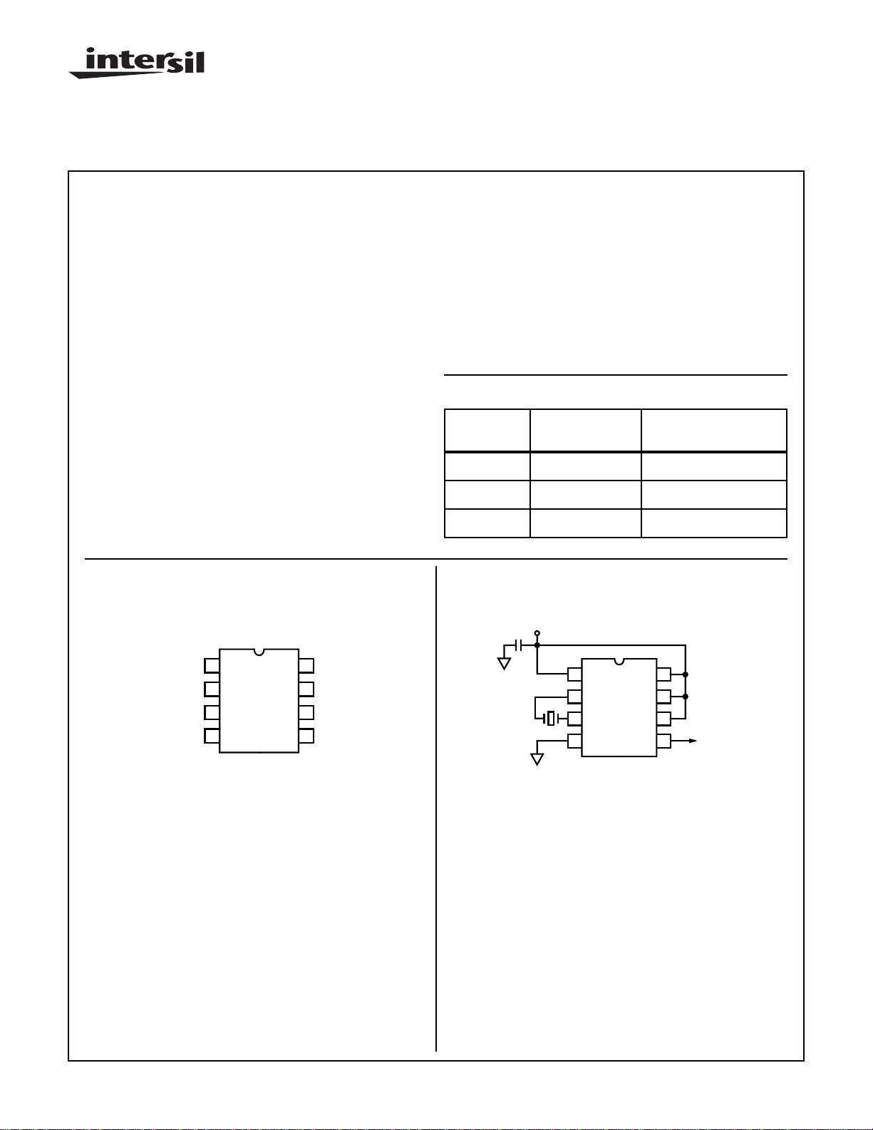
Pinout
V
DD
OSC IN
OSC OUT
V
SS
CDP6872 (PDIP, SOIC)
TOP VIEW
1
2
3
4
8
7
6
5
ENABLE
FREQ 2
FREQ 1
OUTPUT
Typical Application Circuit
V
DD
0.1µf
1
2
32.768kHz
CRYSTAL
32.768kHz MICROPOWER CLOCK OSCILLATOR
CDP6872
3
4
8
7
6
32.768kHz
5
CLOCK
CAUTION: These devices are sensitive to electrostatic discharge; follow proper IC Handling Procedures.
http://www.intersil.com or 407-727-9207
| Copyright © Intersil Corporation 1999
1
File Number 4069
Simplified Block Diagram
V
DD
(NOTE 1)
1
8
ENABLE
CDP6872
EXTERNAL CRYSTAL
FREQ 1
FREQ 2
VDD - 1.4V
VDD - 2.2V
VDD - 3.0V
VDD - 3.8V
V
DD
6
V
DD
7
I
BIAS
V
DD
(NOTE 1)
(NOTE 1)
S1a
S2
1 OF 4
DECODE
S3
S4
15pF
V
RN
+
-
BUFFER AMP
OSC IN 2 3 OSC OUT
S1b S1c
R
F
15pF
V
DD
IN
P
R
F
OSCILLATOR
V
DD
V
DD
LEVEL
SHIFTER
V
RN
4
V
SS
V
DD
P
OUT
N
V
RN
OUTPUT
5
BUFFER
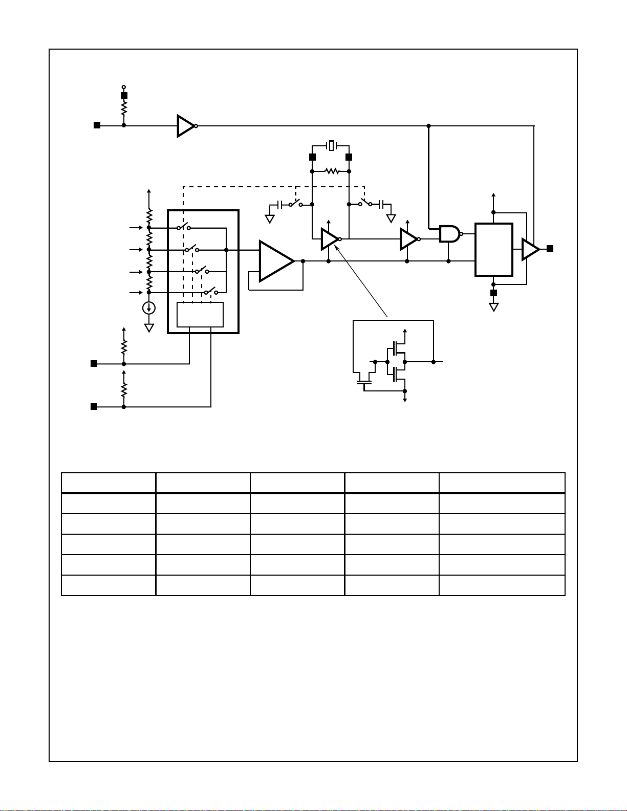
FREQUENCY SELECTION TRUTH TABLE
ENABLE FREQ 1 FREQ 2 SWITCH OUTPUT RANGE
1 1 1 S1a, b, c 10kHz - 100kHz
1 1 0 S2 100kHz - 1MHz
1 0 1 S3 1MHz - 5MHz
1 0 0 S4 5MHz - 10MHz+
0 X X X High Impedance
NOTE:
1. Logic input pull-up resistors are constant current source of 0.4µA.
2
Specifications CDP6872
Absolute Maximum Ratings Operating Conditions
Supply Voltage . . . . . . . . . . . . . . . . . . . . . . . . . . . . . . . . . . . . .10.0V
Voltage (any pin). . . . . . . . . . . . . . . . . . . . . . .VSS-0.3V to VDD+0.3V
Junction Temperature (Plastic Package) . . . . . . . . . . . . . . . +150oC
ESD Rating (Note 2). . . . . . . . . . . . . . . . . . . . . . . . . . . . . . . >4000V
Lead Temperature (Soldering 10s). . . . . . . . . . . . . . . . . . . . +300oC
(SOIC - Lead Tip Only)
CAUTION: Stresses above those listed in “Absolute Maximum Ratings” may cause permanent damage to the device. This is a stress only rating and operation
of the device at these or any other conditions above those indicated in the operational sections of this specification is not implied.
Operating Temperature (Note 3) . . . . . . . . . . . . . . . .-40oC to +85oC
Storage Temperature Range. . . . . . . . . . . . . . . . . .-65oC to +150oC
Thermal Information (Typical)
Thermal Resistance (oC/W) θ
8 Lead Plastic DIP. . . . . . . . . . . . . . . . . . . . . . . . . . . . 125
8 Lead Plastic SOIC . . . . . . . . . . . . . . . . . . . . . . . . . . 170
JA
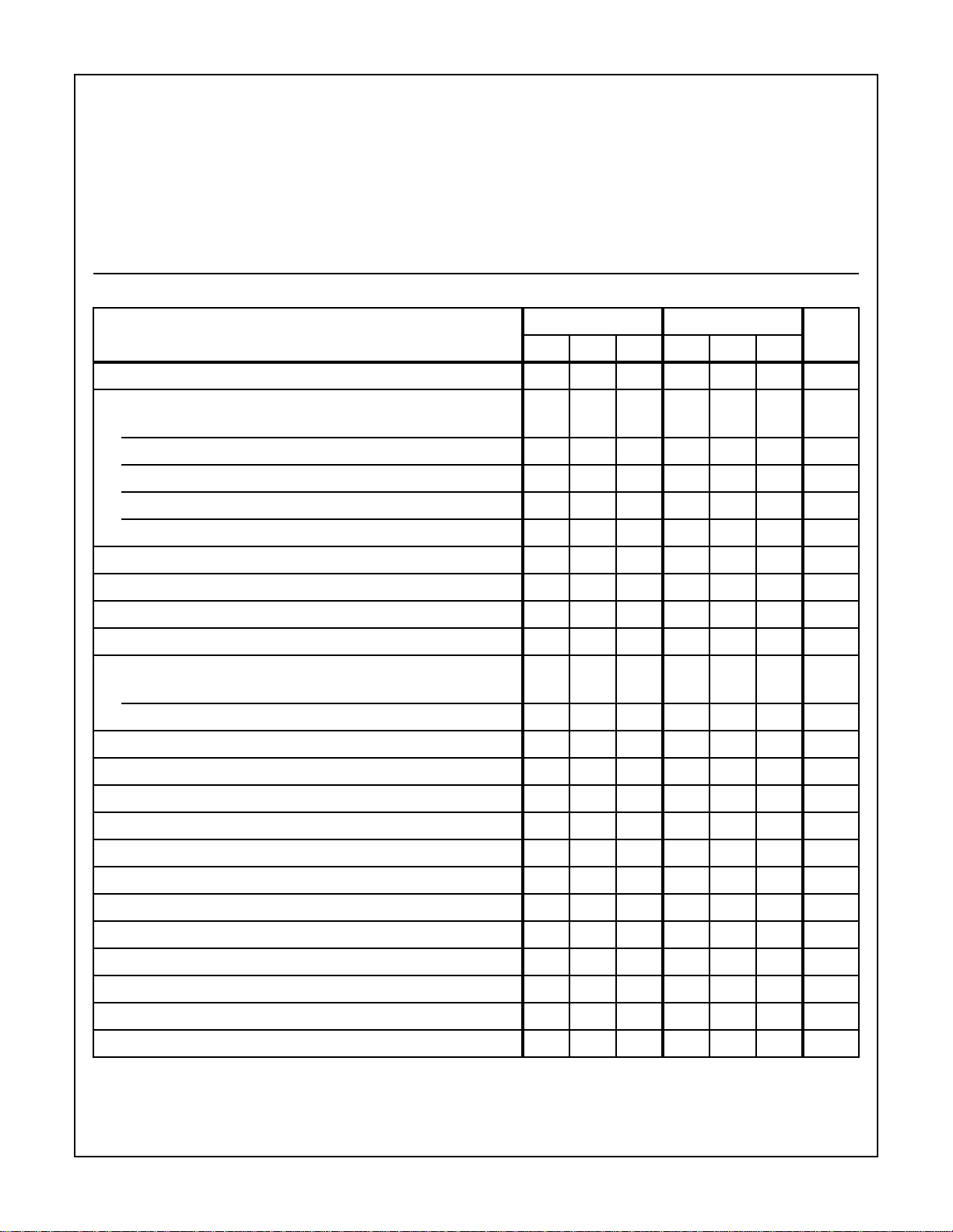
Electrical Specifications V
= GND, TA = +25oC, Unless Otherwise Specified
SS
VDD= 5V VDD = 3V
PARAMETER
VDD Supply Range (f
= 32kHz) 2 5 7 - - - V
OSC
IDD Supply Current
f
= 32kHz, EN = 0 Standby - 5.0 9.0 - - - µA
OSC
f
= 32kHz, CL = 10pF (Note 1), EN = 1, Freq1 = 1, Freq2 = 1 - 5.2 10.2 - 3.6 6.1 µA
OSC
f
= 32kHz, CL = 40pF, EN = 1, Freq1 = 1, Freq2 = 1 - 10 15 - 6.5 9 µA
OSC
f
= 1MHz, CL = 10pF (Note 1), EN = 1, Freq1 = 0, Freq2 = 1 - 130 200 - 90 180 µA
OSC
f
= 1MHz, CL = 40pF, EN = 1, Freq1 = 0, Freq2 = 1 - 270 350 - 180 270 µA
OSC
VOH Output High Voltage (I
VOL Output Low Voltage (I
IOH Output High Current (V
IOL Output Low Current (V
= -1mA) 4.0 4.9 - - 2.8 - V
OUT
= 1mA) - 0.07 0.4 - 0.1 - V
OUT
≥ 4V) - -10 -5 - - - mA
OUT
≤ 0.4V) 5.0 10.0 ----mA
OUT
Three-State Leakage Current
(V
= 0V, 5V, TA = 25oC, -40oC) -0.1----nA
OUT
(V
= 0V, 5V, TA = 85oC) -10----nA
OUT
IIN Enable, Freq1, Freq2 Input Current (VIN = VSS to VDD) - 0.4 1.0 - - - µA
UNITSMIN TYP MAX MIN TYP MAX
VIH Input High Voltage Enable, Freq1, Freq2 2.0 ----- V
VIL Input Low Voltage Enable, Freq1, Freq2 - - 0.8 - - - V
Enable Time (CL = 18pF, RL = 1kΩ) -800----ns
Disable Time (CL = 18pF, RL = 1kΩ) -90----ns
tR Output Rise Time (10% - 90%, f
tF Output Fall Time (10% - 90%, f
Duty Cycle (CL = 40pF) f
Duty Cycle (CL = 40pF) f
= 1MHz, Packaged Part Only (Note 4) 40 54 60 - - - %
OSC
= 32kHz, (See Typical Curves) - 41 - - 44 - %
OSC
Frequency Stability vs. Supply Voltage (f
Frequency Stability vs. Temperature (f
Frequency Stability vs. Load (f
= 32kHz, CL = 40pF) - 12 25 - 12 - ns
OSC
= 32kHz, CL = 40pF) - 12 25 - 14 - ns
OSC
= 32kHz, VDD = 5V, CL=10pF) - 1 ----ppm/V
OSC
= 32kHz, VDD = 5V, CL=10pF) - 0.1 ----ppm/oC
OSC
= 32kHz, VDD = 5V, CL=10pF) - 0.01 ----ppm/pF
OSC
NOTES:
1. Calculated using the equation IDD = IDD (No Load) + (VDD) (f
OSC
)(CL)
2. Human body model.
3. This product is production tested at +25oC only.
4. Duty cycle will vary with supply voltage, oscillation frequency, and parasitic capacitance on the crystal pins.
3
CDP6872
Test Circuits
+5V
0.1µF
1V
P-P
50Ω
1000pF
1
2
CDP6872
3
4
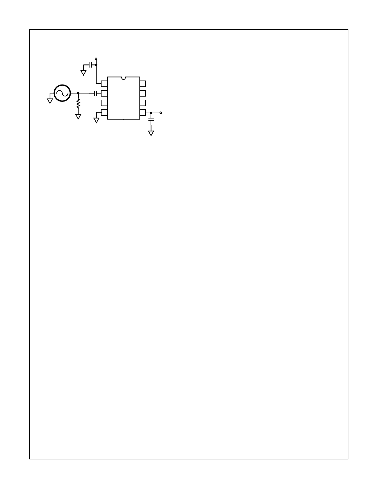
FIGURE 1.
ENABLE
8
FREQ 2
7
FREQ 1
6
5
C
L
18pF
V
OUT
In production the CDP6872 is tested with a 32kHz and a
1MHz crystal. However for characterization purposes data
was taken using a sinewave generator as the frequency
determining element, as shown in Figure 1. The 1V
P-P
input
is a smaller amplitude than what a typical crystal would generate so the transitions are slower. In general the Generator
data will show a “worst case” number for I
, duty cycle, and
DD
rise/fall time. The Generator test method is useful for testing
a variety of frequencies quickly and provides curves which
can be used for understanding performance trends. Data for
the CDP6872 using crystals has also been taken. This data
has been overlaid onto the generator data to provide a reference for comparison.
Theory of Operation
The CDP6872 is a Pierce Oscillator optimized for low power
consumption, requiring no external components except for a
bypass capacitor and a Parallel Mode Crystal. The Simplified Block Diagram shows the Crystal attached to pins 2 and
3, the Oscillator input and output. The crystal drive circuitry
is detailed showing the simple CMOS inverter stage and the
P-channel device being used as biasing resistor R
inverter will operate mostly in its linear region increasing the
amplitude of the oscillation until limited by its transconductance and voltage rails, V
biasing using R
to center the oscillating waveform at the
F
and VRN. The inverter is self
DD
input threshold. Do not interfere with this bias function with
external loads or excessive leakage on pin 2. Nominal value
for R
is 17MΩ in the lowest frequency range to 7MΩ in the
F
highest frequency range.
The CDP6872 optimizes its power for 4 frequency ranges
selected by digital inputs Freq1 and Freq2 as shown in the
Block Diagram. Internal pull up resistors (constant current
0.4µA) on Enable, Freq1 and Freq2 allow the user simply to
leave one or all digital inputs not connected for a corresponding “1” state. All digital inputs may be left open for
10kHz to 100kHz operation.
A current source develops 4 selectable reference voltages
through series resistors. The selected voltage, V
ered and used as the negative supply rail for the oscillator
, is buff-
RN
. The
F
section of the circuit. The use of a current source in the reference string allows for wide supply variation with minimal
effect on performance. The reduced operating voltage of the
oscillator section reduces power consumption and limits
transconductance and bandwidth to the frequency range
selected. For frequencies at the edge of a range, the higher
range may provide better performance.
The OSC OUT waveform on pin 3 is squared up through a
series of inverters to the output drive stage. The Enable
function is implemented with a NAND gate in the inverter
string, gating the signal to the level shifter and output stage.
Also during Disable the output is set to a high impedance
state useful for minimizing power during standby and when
multiple oscillators are OR'd to a single node.
Design Considerations
The low power CMOS transistors are designed to consume
power mostly during transitions. Keeping these transitions
short requires a good decoupling capacitor as close as possible to the supply pins 1 and 4. A ceramic 0.1µF is recommended. Additional supply decoupling on the circuit board
with 1µF to 10µF will further reduce overshoot, ringing and
power consumption. The CDP6872, when compared to a
crystal and inverter alone, will speed clock transition times,
reducing power consumption of all CMOS circuitry run from
that clock.
Power consumption may be further reduced by minimizing
the capacitance on moving nodes. The majority of the power
will be used in the output stage driving the load. Minimizing
the load and parasitic capacitance on the output, pin 5, will
play the major role in minimizing supply current. A secondary
source of wasted supply current is parasitic or crystal load
capacitance on pins 2 and 3. The CDP6872 is designed to
work with most available crystals in its frequency range with
no external components required. Two 15pF capacitors are
internally switched onto crystal pins 2 and 3 to compensate
the oscillator in the 10kHz to 100kHz frequency range.
The supply current of the CDP6872 may be approximately
calculated from the equation:
I
= IDD(Disabled) + VDD × F
DD
where: IDD = Total supply current
V
= Total voltage from VDD (pin1) to VSS (pin4)
DD
F
= Frequency of Oscillation
OSC
C
= Output (pin5) load capacitance
L
Example #1:
= 5V, F
V
DD
I
(Disabled) = 4.5µA (Figure 10)
DD
I
= 4.5µA + (5V)(100kHz)(30pF) = 19.5µA
DD
Measured I
= 100kHz, CL = 30pF
OSC
= 20.3µA
DD
Example #2:
= 5V, F
V
DD
I
(Disabled) = 75µA (Figure 9)
DD
I
= 75µA + (5V)(5MHz)(30pF) = 825µA
DD
Measured I
= 5MHz, CL = 30pF
OSC
= 809µA
DD
OSC
× C
L
4
CDP6872
Crystal Selection
For general purpose applications, a Parallel Mode Crystal is
a good choice for use with the CDP6872. However for
applications where a precision frequency is required, the
designer needs to consider other factors.
Crystals are available in two types or modes of oscillation,
Series and Parallel. Series Mode crystals are manufactured
to operate at a specified frequency with zero load capacitance and appear as a near resistive impedance when oscillating. Parallel Mode crystals are manufactured to operate
with a specific capacitive load in series, causing the crystal
to operate at a more inductive impedance to cancel the load
capacitor. Loading a crystal with a different capacitance will
“pull” the frequency off its value.
The CDP6872 has 4 operating frequency ranges. The higher
three ranges do not add any loading capacitance to the
oscillator circuit. The lowest range, 10kHz to 100kHz, automatically switches in two 15pF capacitors onto OSC IN and
OSC OUT to eliminate potential start-up problems. These
capacitors create an effective crystal loading capacitor equal
to the series combination of these two capacitors. For the
CDP6872, in the lowest range, the effective loading capacitance is 7.5pF. Therefore the choice for a crystal, in this
range, should be a Parallel Mode crystal that requires a
7.5pF load.
In the higher 3 frequency ranges, the capacitance on OSC
IN and OSC OUT will be determined by package and layout
parasitics, typically 4 to 5pF. Ideally the choice for crystal
should be a Parallel Mode set for 2.5pF load. A crystal manufactured for a different load will be “pulled” from its nominal
frequency (see Crystal Pullability).
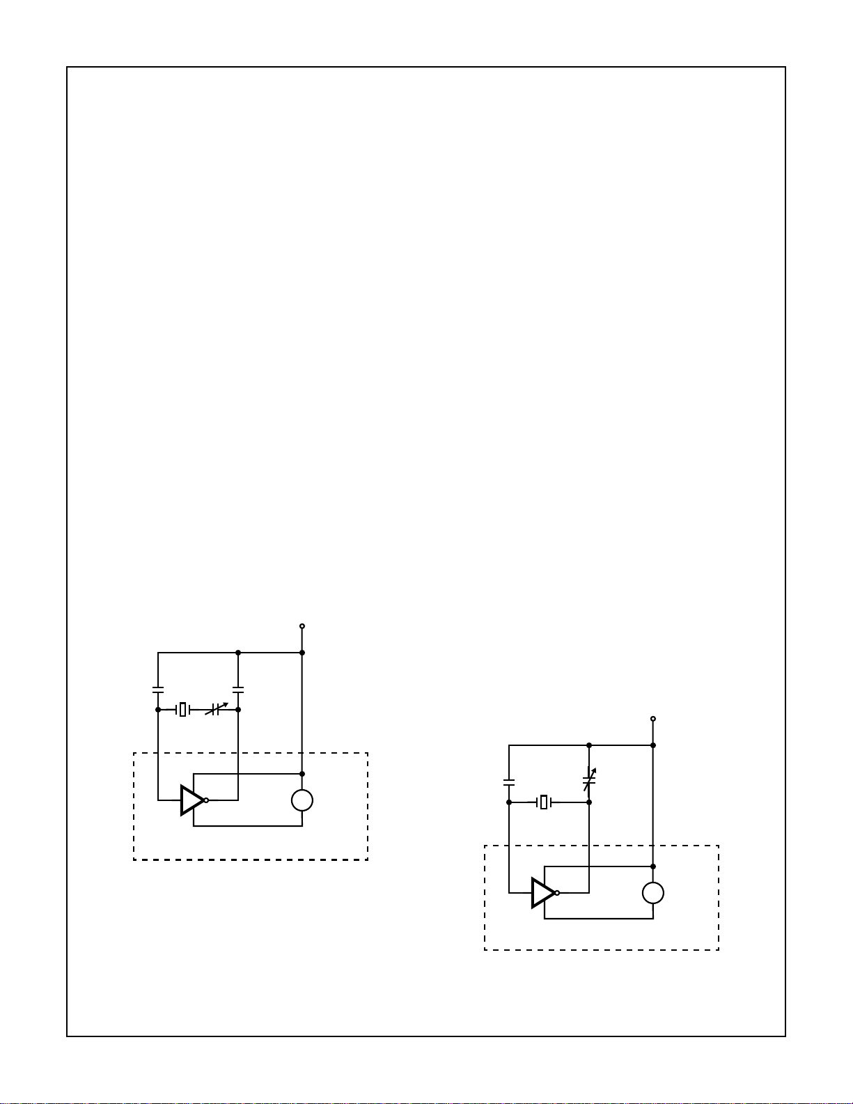
+5V
C
1
C
2
Frequency Fine Tuning
Two Methods will be discussed for fine adjustment of the
crystal frequency. The first and preferred method (Figure 2),
provides better frequency accuracy and oscillator stability
than method two (Figure 3). Method one also eliminates
start-up problems sometimes encountered with 32kHz tuning fork crystals.
For best oscillator performance, two conditions must be met:
the capacitive load must be matched to both the inverter and
crystal to provide ideal conditions for oscillation, and the frequency of the oscillator must be adjustable to the desired
frequency. In Method two these two goals can be at odds
with each other; either the oscillator is trimmed to frequency
by de-tuning the load circuit, or stability is increased at the
expense of absolute frequency accuracy.
Method one allows these two conditions to be met independently. The two fixed capacitors, C
mum load to the oscillator and crystal. C
frequency at which the circuit oscillates without appreciably
changing the load (and thus the stability) of the system.
Once a value for C
has been determined for the particular
3
type of crystal being used, it could be replaced with a fixed
capacitor. For the most precise control over oscillator frequency, C
should remain adjustable.
3
This three capacitor tuning method will be more accurate
and stable than method two and is recommended for 32kHz
tuning fork crystals; without it they may leap into an overtone
mode when power is initially applied.
Method two has been used for many years and may be preferred in applications where cost or space is critical. Note
that in both cases the crystal loading capacitors are connected between the oscillator and V
AC ground. The Simplified Block Diagram shows that the
oscillating inverter does not directly connect to V
erenced to V
and VRN. Therefore VDD is the best AC
DD
ground available.
and C2, provide the opti-
1
; do not use VSS as an
DD
adjusts the
3
but is ref-
SS
XTAL C
2
OSC IN
3
3
OSC OUT
CDP6872
FIGURE 2.
+5V
1
V
DD
+
VREG
-
C
1
2
OSC IN
XTAL
C
2
3
OSC OUT
CDP6872
FIGURE 3.
1
V
DD
+
VREG
-
5
 Loading...