Intersil Corporation CDP1879C-1, CDP1879 Datasheet
CDP1879,
CDP1879C-1
March 1997
Features
• CPU Interface for Use with General-Purpose
Microprocessors
• Time Of Day/Calendar
• Reads Seconds, Minutes, Hours
• Reads Day of Month and Month
• Alarm Circuit With Seconds, Minutes or Hours
Operation
• Power Down Mode
• Separate Clock Output Selects 1 of 15 Square Wave
Signals
• Interrupt Output Activated By Clock Output and/or
Alarm Circuit
• Date Integrity Sampling for Clock Rollover Eliminated
• On-Board Oscillator:
- Crystal Operation CDP1879 at 10V. . . . . . . 4.19MHz,
2.09MHz or 1.048MHz
- Crystal Operation CDP1879C-1 at 5V . . . . . 4.19MHz,
2.09MHz or 1.048MHz or 32kHz
- External Clock Operation at 10V or 5V. . . . 4.19MHz,
2.09MHz, 1.048MHz or 32kHz
• Addressable in Memory Space or CDP1800 Series I/O
Mode
• Low Standby (Timekeeping) Voltage with External Clock
• Related Literature
- AN7275, Guide to the Use of CD1879 and
CDP1879C1 Real Time Clock
Pinout
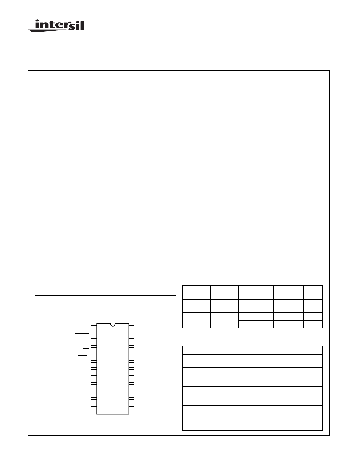
CDP1879, CDP1879C-1 (PDIP, SBDIP)
TOP VIEW
INT
RESET
POWER DOWN
RD
MEM
IO/
TPB/
WR
TPA
CS
A2
A1
A0
V
SS
1
2
3
4
5
6
7
8
9
10
11
12
24
V
DD
XTAL
23
22
XTAL
CLK
21
OUT
DB7
20
DB6
19
DB5
18
DB4
17
DB3
16
DB2
15
DB1
14
DB0
13
CMOS Real-Time Clock
Description
The CDP1879 real-time clock supplies time and calendar information
from seconds to months in BCD format. It consists of 5 separately
addressable and programmable counters that divide down an oscillator
input. The clock input can have any one of 4 possible frequencies,
allowing flexibility in the choice of crystal or external clock sources.
Using an external 32kHz clock source, timekeeping can be performed
down to 2.5V (see Standby (Timekeeping)Voltage Operation).
The device can be memory-mapped for use with any general-purpose
microprocessor and has the additional capability of operating in the
CDP1800 series input/output mode.
The real-time clock functions as a time-of-day/calendar with an alarm
capability that can be set for combinations of seconds, minutes or
hours. Alarm time is configured by loading alarm latches that activate
an interrupt output through a comparator when the counter and alarm
latch v alues are equal.
Fifteen selectable square-wave signals are available as a separate
clock output signal and can also activate the interrupt output. A status
register is available to indicate the interrupt source. The value in an 8 bit
control register determines the operational characteristics of the de vice,
by selecting the prescaler divisor and the clock output, and controls the
load and alarm functions.
A transparent “freeze” circuit preclude clock rollover during counter and
latch access times to assure stable and accurate values in the counters
and alarm latches.
The CDP1879 is functionally identical to the CDP1879C-1. The
CDP1879 has a recommended operating voltage range of 4V to 10.5V,
and the CDP1879C-1 has a recommended operating voltage range of
4V to 6.5V . The CDP1879 and the CDP1879C-1 are supplied in 24 lead
hermetic dual-in-line side-brazed ceramic packages (D suffix) and 24
lead dual-in-line plastic packages (E suffix
Ordering Information
TEMP
P A CKAGE
PDIP -40oC to
SBDIP -40oC to
Burn-In CDP1879CD1X - D24.6
RANGE 5V 10V
CDP1879CE1 CDP1879E E24.6
+85oC
CDP1879CD1 - D24.6
+85oC
CDP1879 Modes of Operation
OPERATION FUNCTION
Read 1. Seconds, minutes, hours, date and month counters
Write 1. Control register to set device operation
Power Down 1. Three-state interrupt output with active alarm or
Interrupt 1. Clock out as source
2. Status register to identify interrupt source
2. Seconds, minutes, hours, date and month counters
3. Alarm latches for alarm time
clock out circuitry for wake-up control
2. Data bus and address inputs are “DON’T CARE”
2. Alarm time as source
3. Either interrupt can occur during normal or power
down mode
).
PKG.
NO.
CAUTION: These devices are sensitive to electrostatic discharge; follow proper IC Handling Procedures.
http://www.intersil.com or 407-727-9207
| Copyright © Intersil Corporation 1999
4-104
File Number
1360.2

CDP1879, CDP1879C-1
Absolute Maximum Ratings Thermal Information
DC Supply Voltage Range, V
(Voltage referenced to VSS Terminal)
CDP1879 . . . . . . . . . . . . . . . . . . . . . . . . . . . . . . . . -0.5V to +11V
CDP1879C-1. . . . . . . . . . . . . . . . . . . . . . . . . . . . . . . -0.5V to +7V
Input Voltage Range, All Inputs . . . . . . . . . . . . . . -0.5 to VDD +0.5V
DC Input Current, Any One Input . . . . . . . . . . . . . . . . . . . . . . ±10mA
Device Dissipation Per Output Transistor. . . . . . . . . . . . . . . . 40mW
For TA = Full Package Temperature Range
(All Package Types)
CAUTION: Stresses above those listed in “Absolute Maximum Ratings” may cause permanent damage to the device. This is a stress only rating and operation
of the device at these or any other conditions above those indicated in the operational sections of this specification is not implied.
DD
Thermal Resistance (Typical) θJA (oC/W) θJC (oC/W)
PDIP Package. . . . . . . . . . . . . . . . . . . 60 N/A
SBDIP Package. . . . . . . . . . . . . . . . . . 50 12
Operating Temperature Range (TA)
Package Type D, H . . . . . . . . . . . . . . . . . . . . . . .-55oC to +125oC
Package Type E. . . . . . . . . . . . . . . . . . . . . . . . . . .-40oC to +85oC
Storage Temperature Range (T
Lead Temperature (During Soldering). . . . . . . . . . . . . . . . . .+265oC
At Distance 1/16 ±1/32 in. (1.59± 0.79mm) From Case for 10s Max
). . . . . . . . . . . .-65oC to +150oC
STG
Operating Conditions at T
PARAMETER
DC Operating Voltage Range 4 10.5 4 6.5 V
Input Voltage Range V
DC Standby (Timekeeping) Voltage (Note 1), V
TA = -40oC to +85oC (Note 2) 3 - 3 - V
TA = 0o to +70oC 2.5 - 2.5 V
Clock Input Rise or Fall Time, tR, t
VDD = 5V - 10 - 10 µs
VDD = 10V - 1 - - µs
NOTES:
1. Timekeeping function only, no READ/WRITE accesses, 32kHz external frequency source only, no crystal operation.
2. See Standby (Timekeeping) Voltage Operation.
= FuIl Package-Temperature Range, Unless Otherwise specified. For maximum reliability, operating con-
A
ditions should be selected so that operation Is always within the following ranges:
LIMITS
CDP1879 CDPl879C-1
MIN MAX MIN MAX
SS
STBY
F
V
DD
V
SS
V
DD
UNITS
V
4-105
CDP1879, CDP1879C-1
XTAL
OSCILLATOR SECOND
XTAL
CLOCK OUT
INT
RESET
V
DD
V
SS
DB0-DB7
A0
A1
A2
TPA
MEM
I-O
TPB/WR
RD
CS
POWER DOWN
PRESCALE
PRESCALE
SELECT
CLOCK AND
INT. LOGIC
INT. STATUS
REGISTER
I/O
INTERFACE
ADDRESS DECODE
AND
CONTROL LOGIC
FREEZE
CIRCUIT
CONTROL
REGISTER
CLOCK
SELECT
AM - PM
AND
HOUR LOGIC
MINUTE HOUR DAY MONTH
8-BIT DATA BUS
COMPARATOR
SECOND
LATCH
MINUTE
LATCH
HOUR
LATCH
CALENDAR
LOGIC
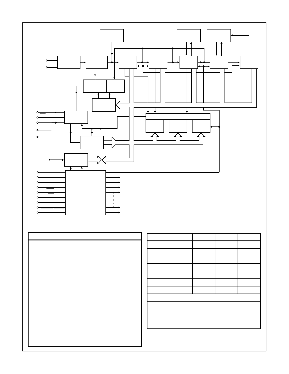
FIGURE 1. REAL-TIME CLOCK FUNCTIONAL DIAGRAM
TABLE 1.
CONTROL REGISTER BIT ASSIGNMENT
Bit 1, 0
Frequency 00
Select 01
10
11
32768Hz
1.048576MHz
2.097152MHz
4.194304MHz
Bit 2
Start/Stop 1 = Start
0 = Stop
Bit 3
Counter/Latch Control
“0” = Write to Counter and disable alarm
“1” = Write to and enable alarm Clock Select
Bit 7, 6, 5, 4
0000 - disableµs
0001 - 488.2µs
0010 - 976.5µs
0011 - 1953.1µs
0100 - 3906.2µs
0101 - 7812.5µs
0110 - 15.625ms
0111 - 31.25ms
1000 - 62.5ms
1001 - 125ms
1010 - 250ms
1011 - 500ms
1100 - sec.
1101 - min.
1110 - hour
1111 - day
TABLE 2.
ADDRESSES A2 A1 A0
Latch, Counter Seconds 0 1 0
Latch, Counter Minutes 0 1 1
Latch, Counter Hours 1 0 0
Counter, Day 1 0 1
Counter, Month 1 1 0
Control, Register 1 1 1
Status Register 1 1 1
MSB of Hours Counters (Bit 7) is an AM-PM Bit. 0 = AM; 1 = PM
Bit 6 of Hours Counter Controls 12/24 hr. 1 = 12 Hr: 0 = 24 Hr.
Status Register: Bit 7 MSB = Alarm
Interrupt Source: Bit 6 = Clock.
MSB of Month Counter (Bit 7) is a Leap Year Bit 0 = No, 1 = Yes.
4-106
CDP1879, CDP1879C-1
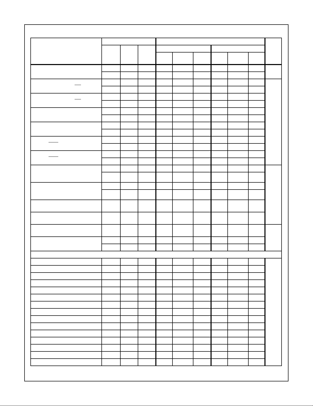
Static Electrical Specifications at T
-40oC to +85oC VDD± 5%, Unless Otherwise Specified
A
CONDITIONS LIMITS
CDP1879 CDPl879C-1
PARAMETER
Ouiescent Device Current I
V
(V)
DD
V
O
(V)
V
IN
DD
(V)
MIN
(NOTE 1)
TYP MAX MIN
(NOTE 1)
TYP MAX
0, 5 5 - 0.01 50 - 0.02 200 µA
0, 10 10 - 1 200 - - -
Output Low Drive (Sink)
Current, Data Bus and INT l
Output High Drive (Source)
Current, Data Bus and INT I
Output Low Drive (Sink)
Current, Clock Out l
Output High Drive (Source)
Current, Clock Out I
Output Low Drive (Sink)
Current, XTAL Out l
Output High Drive (Source)
Current, XTAL Out I
Output Voltage
Low-Level V
(Note 2)
Output Voltage
High Level V
(Note 2)
Input Low Voltage V
Input High Voltage V
Input Leakage Current I
Three-State Output
Leakage Current I
OL
OH
OL
OH
OL
OH
OL
OH
IL
IH
IN
OUT
0.4 0, 5 5 1.8 4 - - - -
0.5 0,10 10 3.6 7 - - - -
4.6 0, 5 5 -1.1 -2.3 - -1.1 -2.3 -
9.5 0,10 10 -2.6 -4.4 - - - -
0.4 0, 5 5 0.6 1.4 - 0.6 1.4 -
0.5 0,10 10 1.2 3 - - - -
4.6 0, 5 5 -1.1 -2.3 - -1.1 -2.3 -
9.5 0,10 10 -2.6 -4.4 - - - -
0.4 0, 5 5 0.2 0.9 - 0.2 0.9 -
0.5 0,10 10 0.4 2 - - - -
4.6 0, 5 5 -0.15 -0.4 - -0.15 -0.4 -
9.5 0,10 10 -0.3 -0.7 - - - -
- 0, 5 5 - 0 0.1 - 0 0.1
- 0,10 10 - 0 0.1 - - -
- 0, 5 5 4.9 5 - 4.9 5 -
- 0, 10 10 9.9 10 - - - -
0.5, 4.5
0.5, 9.5
0.5, 4.5
0.5, 9.5
Any
Input
-
-
-
-
0, 5
0, 10
10
10
10
5
5
5
3.5
-
-
7
-
-
-
-
-
-
-
-
1.5
±1
±2
-
3
-
-
-
3.5
-
-
-
-
-
-
-
-
-
0, 5 0,5 5 - - ±1- - ±1
0,10 0,10 10 - - ±1--Operating Current (Note 3)
External Clock 32kHz - - 5 - 0.01 0.15 - 0.01 0.15
External Clock 1MHz - - 5 - 0.2 1 - 0.2 1
External Clock 2MHz - - 5 - 0.35 1.5 - 0.35 1.5
External Clock 4MHz - - 5 - 0.7 2 - 0.7 2
External Clock 32kHz - - 10 - 0.03 0.25 - - External Clock 1MHz - - 10 - 0.4 2 - - External Clock 2MHz - - 10 - 0.8 3 - - External Clock 4MHz - - 10 - 1.6 4.5 - XTAL Oscillator (Note 4) 32kHz - - 5 - 0.1 0.25 - 0.1 0.25
XTAL Oscillator (Note 4) 1MHz - - 5 - 0.3 0.5 - 0.3 0.5
XTAL Oscillator (Note 4) 2MHz - - 5 - 0.4 0.6 - 0.4 0.6
XTAL Oscillator (Note 4) 4MHz - - 5 - 0.6 0.8 - 0.6 0.8
XTAL Oscillator (Note 4) 1MHz - - 10 - 1.6 3 - - XTAL Oscillator (Note 4) 2MHz - - 10 - 1.8 3.5 - - XTAL Oscillator (Note 4) 4MHz - - 10 - 2 5 - - -
UNITS
mA
V
1.5
-
-
-
±1
µA
mA
4-107
CDP1879, CDP1879C-1
Static Electrical Specifications at T
-40oC to +85oC VDD± 5%, Unless Otherwise Specified (Continued)
A
CONDITIONS LIMITS
PARAMETER
Input Capacitance C
Output Capacitance C
IN
OUT
Maximum Clock Rise tR, t
and Fall Times
V
(V)
- - - - 5 7.5 - 5 7.5 pF
- - - - 10 15 - 10 15
F
--5--10--10µs
--10--1---
V
O
(V)
V
IN
DD
(V)
NOTES:
1. Typical values are for TA = 25oC and nominal VDD.
2. IOL = IOH = 1µA.
3. Operating current measured with clockout = 488.2µs and no load.
4. See Table 3 and Figure 6 for oscillator circuit information.
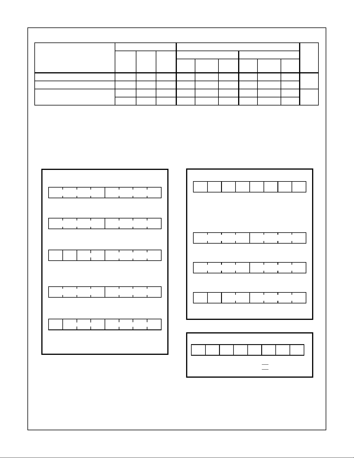
Programming Model
WRITE AND READ REGISTERS WRITE ONLY REGISTERS
BCD FORMAT
DB7 DB0
TENS 0-5 UNITS 0-9
SECONDS COUNTER (00-59)
DB7 DB0
TENS 0-5
MINUTES COUNTER (00-59)
DB7 DB0
DB6
X X TENS 0-2
HOURS COUNTER (01 - 12 OR 00-23)
DB7 0=AM, 1=PM
DB6 0=24 HR, 1=12 HR
DB7 DB0
TENS 0-3 UNITS 0-9
DAY OF MONTH COUNTER
(01-28, 29, 30, 31)
DB7 DB0
X TENS 0 OR 1
MONTH COUNTER
(JAN=1 DEC=12)
DB7 0=NO LEAP YEAR
1=LEAP YEAR
UNITS 0-9
UNITS 0-9
UNITS 0-9
CDP1879 CDPl879C-1
(NOTE 1)
MIN
TYP MAX MIN
DB7 DB0
7
6543210
CONTROL REGISTER
DB0-DB1 - FREQUENCY SELECT
DB2 - START/STOP
DB3 - COUNTER/ALARM LATCH CONTROL
DB4-DB7 - CLOCK OUTPUT SELECT
DB7 DB0
TENS 0-5 UNITS 0-9
SECONDS ALARM LATCH (00-59)
DB7 DB0
TENS 0-5 UNITS 0-9
MINUTES ALARM LATCH (00-59)
DB6
DB7 DB0
TENS 0-2 UNITS 0-9XX
HOURS ALARM LATCH (01-12 OR 00-23
12 HR, DB7=0 AM, 1=PM
24 HR, DB7=X
(NOTE 1)
TYP MAX
READ ONLY REGISTER
DB7 DB0
DB6
X
X000000
UNITS
4-108
INTERRUPT STATUS REGISTER
DB7=1 ALARM CIRCUIT ACTIVATED INT.
DB6=1 CLOCK OUTPUT ACTIVATED
INT.
CDP1879, CDP1879C-1
REGISTER TRUTH TABLE
ADDRESS ACTIVE SIGNAL
0 1 0 X - 0 Write Seconds Counter
0 1 0 - X 0 Read Seconds Counter
0 1 1 X - 0 Write Minutes Counter
0 1 1 - X 0 Read Minutes Counter
1 0 0 X - 0 Write Hours Counter
1 0 0 - X 0 Read Hours Counter
1 0 1 X - 0 Write Date Counter
1 0 1 - X 0 Read Date Counter
1 1 0 X - 0 Write Month Counter
1 1 0 - X 0 Read Month Counter
0 1 0 X - 1 Write Seconds Alarm Latch
0 1 1 X - 1 Write Minutes Alarm Latch
1 0 0 X - 1 Write Hours Alarm Latch
1 1 1 X - - Write Control Register
BIT 3 CONTROL
REGISTER REGISTER OPERATIONA2 A1 AO TPB/WR RD
1 1 1 - X - Read Int. Status Register
General Operation
The real-time clock contains seconds, minutes, and hours,
date and month counters that hold time of day/calendar
information (see Figure 2). The frequency of an intrinsic
oscillator is divided down to supply a once-a-second signal
to the counter series string. The counters are separately
addressable and can be written to or read from.
The real-time clock contains seconds, minutes and hour
write-only alarm latches that store the alarm time (see Figure 3). When the value of the alarm latches and counters are
equal, the interrupt output is activated. The interrupt output
can also be activated by a clock output transition. The clock
output is derived from the prescaler and counters and can
be one of 15 square-wave signals. The value in the readonly interrupt status register identifies the interrupt source.
Operational control of the real-time clock is determined by
the byte in a write-only control register. The 8-bit v alue in this
register determines the correct divisor for the prescaler, a
data direction and alarm enable bit, clock output select, and
start/stop control (see Figure 4).
Data transfer and addressing are accomplished in two
modes of operation, memory mapping and I/O mapping
using the CDP1800-series microprocessors. The mode is
selected by the level on an input pin. (IO/
mapping implies use of the address lines as chip selects and
address inputs during linear selection or partial or full decoding methods. I/O mapping with the CDP1800-series microprocessors involves use of the N line outputs in conjunction
with input and output instructions to transfer data to and from
memory.
MEM). Memory
4-109
 Loading...