

CDP1878C
March 1997
Features
• Compatible with General Purpose and CDP1800
Series Microprocessor Systems
• Two 16-Bit Down Counters and Two 8-Bit Control
Registers
• 5 Modes Including a Versatile Variable-Duty Cycle
Mode
• Programmable Gate-Level Select
• Two-Complemented Output Pins for Each CounterTimer
• Software-Controlled Interrupt Output
• Addressable in Memory Space or CDP1800-Series I/O
Space
Ordering Information
PART
NUMBER TEMP. RANGE PACKAGE PKG. NO.
CDP1878CE -40oC to +85oC PDIP E28.6
CDP1878CD -40oC to +85oC SBDIP N28.6
CMOS Dual Counter-Timer
Description
The CDP1878C is a dual counter-timer consisting of two 16bit programmable down counters that are independently
controlled by separate control registers. The value in the registers determine the mode of operation and control functions. Counters and registers are directly addressable in
memory space by any general industry type microprocessors, in addition to input/output mapping with the CDP1800
series microprocessors.
Each counter-timer can be configured in five modes with the
additional flexibility of gate-level control. The control registers in addition to mode formatting, allow software start and
stop, interrupt enable, and an optional read control that
allows a stable readout from the counters. Each countertimer has software control of a common interrupt output with
an interrupt status register indicating which counter-timer
has timed out.
In addition to the interrupt output, true and complemented
outputs are provided for each counter-timer for control of
peripheral devices.
This type is supplied in 28-lead dual-in-line ceramic packages (D suffix), and 28-lead dual-in-line plastic packages (E
suffix).
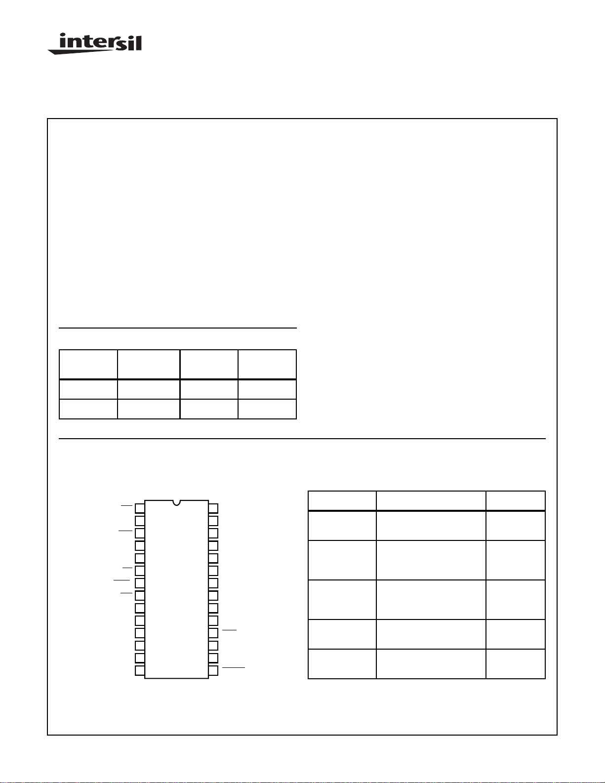
Pinout
IO/
TPB/
INT
TAO
TAO
TAG
TACL
MEM
WR
TPA
V
RD
CS
A0
A1
A2
SS
1
2
3
4
5
6
7
8
9
10
11
12
13
14
CDP1878C
(DIP)
TOP VIEW
28
27
26
25
24
23
22
21
20
19
18
17
16
15
V
DD
DB7
DB6
DB5
DB4
DB3
DB2
DB1
DB0
TBO
TBO
TBG
TBCL
RESET
TABLE 1. MODE DESCRIPTION
MODE FUNCTION APPLICA TION
1 Timeout Outputs change when clock
decrements counter to “0”
2 Timeout
Strobe
3 Gate-Con-
trolled One
Shot
4 Rate Generator Repetitive clockwide output
5 Variable-Duty
Cycle
One clockwide output pulse
when clock decrements
counter to “0”
Outputs change when clock
decrements counter to “0”.
Retriggerable
pulse
Repetitive output with
programmed duty cycle
Event counter
Trigger pulse
Time-delay
generation
Time-base
generator
Motor control
CAUTION: These devices are sensitive to electrostatic discharge; follow proper IC Handling Procedures.
http://www.intersil.com or 407-727-9207
| Copyright © Intersil Corporation 1999
4-91
File Number 1341.2
CDP1878C
Absolute Maximum Ratings Thermal Information
DC Supply-Voltage Range, (VDD)
(All Voltages Referenced to VSSTerminal)
CDP1878C . . . . . . . . . . . . . . . . . . . . . . . . . . . . . . . . . -0.5V to +7V
Input Voltage Range, All Inputs . . . . . . . . . . . . .-0.5V to VDD +0.5V
DC Input Current, Any One Input. . . . . . . . . . . . . . . . . . . . . . . . .±10mA
CAUTION: Stresses above those listed in “Absolute Maximum Ratings” may cause permanent damage to the device. This is a stress only rating and operation
of the device at these or any other conditions above those indicated in the operational sections of this specification is not implied.
Thermal Resistance (Typical) θJA (oC/W) θJC (oC/W)
PDIP Package. . . . . . . . . . . . . . . . . . . 55 N/A
SBDIP Package. . . . . . . . . . . . . . . . . . 50 12
Device Dissipation Per Output Transistor
TA = Full Package Temperature Range
(All Package Types). . . . . . . . . . . . . . . . . . . . . . . . . . . . . . 100mW
Operating Temperature Range (TA)
Package Type D. . . . . . . . . . . . . . . . . . . . . . . . . .-55oC to +125oC
Package Type E. . . . . . . . . . . . . . . . . . . . . . . . . . .-40oC to +85oC
Storage Temperature Range (T
). . . . . . . . . . . .-65oC to +150oC
STG
Lead Temperature (During Soldering)
At distance 1/16 ± 1/32 In. (1.59 ± 0.79mm)
from case for 10s max. . . . . . . . . . . . . . . . . . . . . . . . . . . . +265oC
Recommended Operating Conditions At T
= Full Package Temperature Range. For maximum reliability, operating conditions
A
should be selected so that operation is always within the following ranges:
PARAMETER SYMBOL MIN MAX UNITS
DC Operating Voltage Range 4 6.5 V
Input Voltage Range V
Maximum Clock Input Rise or Fall Time tR, t
Minimum Clock Pulse Width tWL, t
Maximum Clock Input Frequency f
Static Electrical Specifications At T
= -40oC to +85oC, VDD± 5% Except as noted:
A
F
WH
CL
SS
-5µs
200 - ns
DC 1 MHz
V
DD
V
CONDITIONS LIMITS
PARAMETER SYMBOL
Quiescent Device Current I
Output Low Drive (Sink) Current I
Output High Drive (Source) Current I
Output Voltage Low-Level (Note 2) V
Output Voltage High-Level (Note 2) V
Input Low Voltage V
Input High Voltage V
Input Leakage Current I
Operating Current (Note 3) I
Input Capacitance C
Output Capacitance C
DD
OL
OH
OL
OH
IL
IH
IN
DD1
IN
OUT
V
O
(V)
- 0, 5 5 - 0.02 200 µA
0.4 0, 5 5 1.6 3.2 - mA
4.6 0, 5 5 -1.15 -2.3 - mA
- 0, 5 5 - 0 0.1 V
- 0, 5 5 4.9 5 - V
0.5, 4.5 - 5 - - 1.5 V
0.5, 9.5 - 5 3.5 - - V
Any Input 0, 5 5 - - ±1 µA
- 0, 5 5 - 1.5 3 mA
---- 57.5pF
----1015pF
V
(V)
IN
V
DD
(V) MIN
(NOTE 1)
TYP MAX
UNITS
NOTES:
1. Typical values are for TA = +25oC and nominal VDD.
2. IOL = IOH = 1µA
3. Operating current measured at 200kHz for VDD = 5V, with open outputs (worst-case frequencies for CDP1802A system operating at maximum speed of 3.2MHz).
4-92
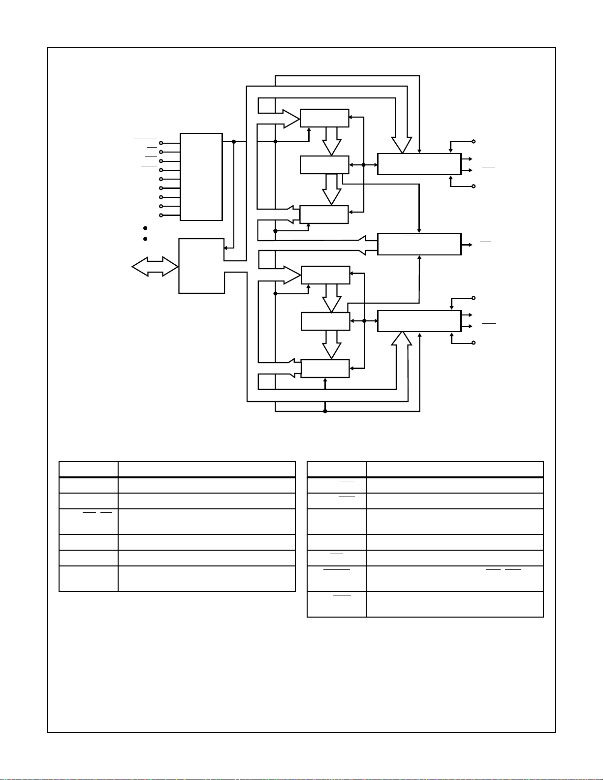
Functional Diagram
CDP1878C
JAM
REGISTER A
8-BIT
EXTERNAL
BUS
RESET
TPB/WR
IO/MEM
V
DD
V
SS
RD
TPA
CS
A2
A1
A0
I-O
CONTROL
AND
LOGIC
DAT A
BUS
DRIVERS
COUNTER A
HOLDING
REGISTER A
JAM
REGISTER B
COUNTER B
HOLDING
REGISTER B
CONTROL REGISTER A
AND MODE CONTROL
INT AND
STATUS REGISTER
CONTROL REGISTER B
AND MODE CONTROL
GATE A
TAO
TAO
CLOCK A
INT
GATE B
TBO
TBO
CLOCK B
FUNCTIONAL DEFINITIONS FOR CDP1878C TERMINALS
TERMINAL USAGE TERMINAL USAGE
VDD - V
Power TAO, TAO Complemented outputs of Timer A
SS
DB0-DB7 Data to and from device TBO, TBO Complemented outputs of Timer B
TPB/WR, RD Directional Control Signals TPA Used with CDP1800-series processors, tied high
otherwise
A0, A1, A2 Addresses that select counters or registers CS Active high input that enables device
TACL, TBCL Clocks used to decrement counters INT Low when counter is “0”
TAG, TBG Gate inputs that control counters RESET When active, TAO, TBO are low, TAO, TBO are
high. Interrupt status register is cleared.
IO/MEM Tied high in CDP1800 input/output mode, other-
wise tied low
4-93
CDP1878C
REGISTER TRUTH TABLE
ADDRESS ACTIVE
REGISTER COUNTERA2 A1 A0 TPB/WR RD
1 1 0 X Write Counter A MSB
1 1 0 X Read Counter A MSB
0 1 0 X Write Counter A LSB
0 1 0 X Read Counter A LSB
1 0 0 X Control Register A
1 1 1 X Write Counter B MSB
1 1 1 X Read Counter B MSB
0 1 1 X Write Counter B LSB
0 1 1 X Read Counter B LSB
1 0 1 X Control Register B
1 0 0 X Interrupt Status Register
101 X
0 0 0 Not Used
0 0 1 Not Used
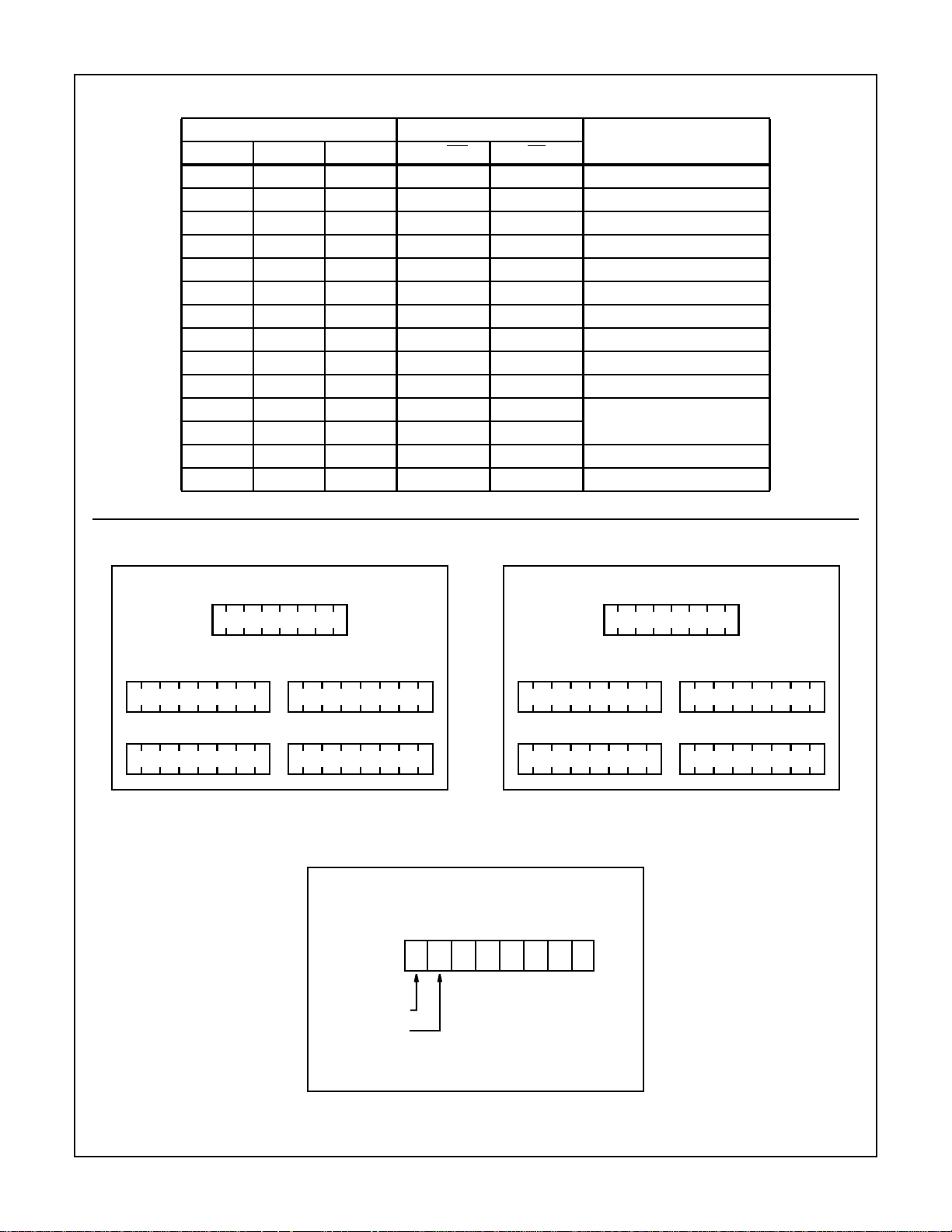
Programming Model
BUS 7
CONTROL REGISTER
WRITE ONLY
HOLDING REGISTER LSB
READ ONLY
HOLDING REGISTER MSB
COUNTER A REGISTERS COUNTER B REGISTERS
BUS 0
JAM REGISTER LSB
WRITE ONLY
JAM REGISTER MSB
HOLDING REGISTER LSB
READ ONLY
HOLDING REGISTER MSB
BUS 7
XX000000
READ ONLY
BUS 0
BUS 7
CONTROL REGISTER
WRITE ONLY
BUS 0
JAM REGISTER LSB
WRITE ONLY
JAM REGISTER MSB
TIMER A
TIMER B
INTERRUPT STATUS REGISTER
4-94

CDP1878C
Functional DescriptIon
The dual counter-timer consists of two programmable 16-bit
down counters, separately addressable and controlled by
two independent 8-bit control registers. The word in the control register determines the mode and type of operation that
the counter-timer performs. Writing to or reading from a
counter or register is enabled by selective addressing during
a write or read cycle. The data is placed on the data bus by
the microprocessor during the write cycle or read from the
counter during the read cycle. Data to and from the counters
and to the control registers is in binary format.
Each counter-timer consists of three parts. The first is the
counter itself, a 16-bit down counter that is decremented on
the trailing edge of the clock input. The second is the jam
register that receives the data when the counter is written to.
The word in the control register determines when the jam
register value is placed into the counter. The third part is the
holding register that places the counter value on the data
bus when the counter is read.
When the counter has decremented to zero, three events
occur. The first involves the common interrupt output pin that,
if enabled, becomes active low. The second is the setting of a
bit in the interrupt status register. This register can be read to
determine which counter-timer has timed out. The third event
is the logic change of the complemented output pins.
In addition to the clock input used to decrement the counter, a
gate input is available to enable or initiate operation. The
counter-timers are independent and can have different mode
operations.
Write Operation
The counters and registers are separately addressable and
are programmed via the data bus when the chip is selected
with the TPB/
the counter jam register be loaded first with the required value
WR pin active. Normal sequencing requires that
(most significant and least significant byte in any order), and
then the control register be accessed and loaded with the
control word. The trailing edge of the TPB/
WR pulse will latch
the control word into the control register. The trailing edge of
the first clock to occur with gate valid will cause the counter to
be jammed with its initial value. The counter will decrement on
the trailing edge of succeeding clocks as long as the gate is
valid, until it reaches zero. The output levels will then change,
and if enabled, the interrupt output will become active and the
appropriate timer bit will be set in the interrupt status register.
The interrupt output and the interrupt status register can be
cleared (to their inactive state) by addressing the control register with the TPB/
WR line active For example, if counter A
times out, control register A must be accessed to reset the
interrupt output high and reset the timer A bit in the status register low . Timer B bit in the status register will be unaffected.
Read Operation
Each counter has a holding register that is continuously
being updated by the counter and is accessed when the
counter is addressed during read cycles. Counter reads are
accomplished by halting the holding register and then reading it, or by reading the holding register directly. If the holding
register is read directly, data will appear on the bus if the
counters are addressed with the
RD line active. However, if
the clock decrements the counter between the two read
operations (most and least significant byte), an inaccurate
value will be read. To preclude this from happening, writing a
“1” into bit 6 of the control register and then addressing and
reading the counter will result in a stable reading. This operation prevents the holding register from being updated by the
counter and does not affect the counter’s operation.
The interrupt status register is read by addressing either
control register with the
RD line active. A “1” in bit 7 indicates
Timer A has timed out and a “1” in bit 6 indicates Timer B
has timed out. Bits 0-5 are zeros.
Control Register
7 6543210
JAM ENABLE
1 = ENABLE
0 = DISABLE
HOLDING REGISTER CONTROL
1 = FREEZE HOLDING REGISTER
0 = UPDATE CONTINUOUSLY
START/STOP CONTROL
1 = START COUNTER
0 = STOP COUNTER
Bits 0, 1 and 2
Mode Selects - See Mode Timing Diagrams (Figures 1, 2, 3,
4, and 5).
Note: When selecting a mode, the timer outputs TAO and TBO
are set low, and
TAO and TBO are set high. If bits 0, 1 and 2
are all zero’s when the control register is loaded, no mode is
selected, and the counter-timer outputs are unaffected. Issuing
mode 6 will cause an indeterminate condition of the counter,
issuing mode 7 is equivalent to issuing mode 5.
MODE SELECT
GATE LEVEL SELECT
1 = POSITIVE (HIGH)
0 = NEGATIVE (LOW)
INTERRUPT ENABLE
1 = ENABLE
0 = DISABLE
Mode 1 - Timeout - 0 0 1
Mode 2 - Timeout Strobe - 0 1 0
Mode 3 - Gate Controlled One Shot 0011
Mode 4 - Rate Generator - 1 0 0
Mode 5 - Variable-Duty Cycle - 1 0 1
No Mode selected. Counter outputs
unaffected
001 = MODE 1
010 = MODE 2
†011 = MODE 3
100 = MODE 4
101 = MODE 5
†PLUS BIT 7 = 0
BIT 7 BIT 2 BIT 1 BIT 0
-000
4-95

CDP1878C
Bit 3 - Gate Level Select - All modes require an enabling signal on the gate to allow counter operation. This enabling signal is either a level or a pulse (edge). Positive gate level or
edge enabling is selected by writing a “1” into this bit and
negative (low) enabling is selected when bit 3 is “0”.
Bit 4 - Interrupt Enable - Setting this bit to “1” enables the
INT output, and setting it to “0” disables it. When reset, the
INT output is at a high level. If the interrupt enable bit in the
control register is enabled and the counter decrements to
zero, the
INT output will go low and will not return high until
the counter-timer is reset or the selected control register is
written to. Example: If timer B times out, control register B
must be accessed to reset the
INT output high. If the interrupt enable bit is set to “0”, the counter’s timeout will ha ve no
effect on the
In mode 5, the variable-duty cycle mode, the
lNT output.
lNT pin will
become active low when the MSB in the counter has decremented to zero.
Bit 5 - Start/Stop Control - This bit controls the clock input to
the counter and must be set to “1” to enable it. Writing a “0”
into this location will halt operation of the counter. Operation
will not resume until the bit is set to “1”.
Bit 6 - Holding Register Control - Since the counter may be
decrementing during a read cycle, writing a “1” into this loca-
tion will hold a stable value in the hold register for subsequent read operations. Rewriting a “1” into bit 6 will cause an
update in the holding register on the next trailing clock edge.
If this location contains a “0”, the holding register will be
updated continuously by the value in the counter.
Bit 7 - Jam Enable - When this bit is set to “1 “during a write
to the control register, the 16-bit value in the jam register will
be available to the counter; TAO and TBO are reset low and
TAO and TBO are set high. On the trailing edge of the first
input clock signal with the gate valid this value will be latched
in the counter, the counter outputs TAO and TBO will be set
high and the
TAO and TBO will be reset low. Setting bit 7 to
“0” will leave the counter value unaffected. This location
should be set to “0” any time a write to the control register
must be performed without changing the present counter
value. If the value in the jam register has not been changed,
writing a “1” into bit 7 of the control register with zeros in bits
0,1, and 2 (mode select) will reload the counter with the old
value and leave the mode unchanged. If the value in the jam
register is changed, then the next write to the control register
(with bit 7 a “1”) must include a valid mode select (i.e., at
least 1 of the bits 0,1, or 2 must be a ”1”).
In mode 3, the hardware start is enabled by writing a “0” into
bit 7. If a “1” is written to bit 7, the timeout will start immediately and mode 3 will resemble mode 1.
Mode Descriptions
MODE CONTROL REGISTER GATE CONTROL
1
Mode 1
After the count is loaded into the jam register and the control
register is written to with the jam-enable bit high on the trailing edge of the first clock after the gate is valid, TXO goes
high and
counter as long as the gate remains valid. When it reaches
zero TXO goes low and
COUNTER VALUE
TXO goes low. The input clock decrements the
TXO goes high, and if enabled, the
CLOCK
WR CONTROL
REGISTER
GATE
Timeout Selectable High or Low
XXXXX001
BUS 7 BUS 0
Level Enables Operation
interrupt output is set low. Writing to the counter while it is
decrementing has no effect on the counter value unless the
control register is subsequently written to with the jamenable bit high. After timeout the counter remains at FFFF
unless reloaded.
0112345
0112345
STALL COUNTER
FFFF
TXO
INT
LOAD COUNT = 5
FIGURE 1. TIMEOUT (MODE 1) TIMING WAVEFORMS
4-96

CDP1878C
MODE CONTROL REGISTER GATE CONTROL
2
Timeout Strobe Selectable High or Low
XXXXX010
BUS 7 BUS 0
Mode 2
Operation of this mode is the same as mode 1, except the
outputs will change for one clock period only and then return
COUNTER VALUE
CLOCK
WR CONTROL
REGISTER
GATE
TXO
INT
FIGURE 2. TIMEOUT STROBE (MODE 2) TIMING WAVEFORMS
NOTE: Write to control register with mode selects = 0
Level Enables Operation
to the condition of TXO high and
reloaded
0123
30123
SEE NOTE
LOAD COUNT = 3
TXO low , and the counter is
1233
0123
MODE CONTROL REGISTER GATE CONTROL
Gate Controlled One-Shot Selectable Positive or
3
0XXXX011
BUS 7 BUS 0
Mode 3
After the jam register is loaded with the required value, the
gate edge will initiate this mode. TXO will be set high, and
TXO will be set low. The clock will decrement the counter.
When zero is reached, TXO will go low and
TXO will be high,
and the interrupt output will be set low. The counter is retrig-
COUNTER VALUE
CLOCK
WR CONTROL
REGISTER
GATE
TXO
INT
LOAD COUNT = 3
Negative Going Edge
Initiates Operation
gerable: While the counter is decrementing, a gate edge or
write to the control register with the jam-enable bit high, will
load the counter with the jam register value and restart the
one-shot operation.
123
0123
2330
1233
FIGURE 3. GATE CONTROLLED ONE-SHOT (MODE 3) TIMING WAVEFORMS
4-97

CDP1878C
MODE CONTROL REGISTER GATE CONTROL
4
Rate Generator Selectable High or Low
XXXXX100
BUS 7 BUS 0
Mode 4
A repetitive clock-wide output pulse will be output, with the
time between pulses equal to the counter’s value, (trailing
edge to leading edge). This model is software started with a
write to the control register if the gate level is valid. If the
counter is written to while decrementing, the new value will
COUNTER VALUE
CLOCK
123
WR CONTROL
REGISTER
GATE
TXO
INT
LOAD COUNT = 3
FIGURE 4. RATE GENERATORS (MODE 4) TIMING WAVEFORMS
Level Enables Operation
not affect the counter’s operation until the present timeout
has concluded, unless the control register is written to with
the jam-enable bit high. If the gate input (TAG or TBG) is
used to start this mode, the first cycle following the gate
going true is indeterminate.
123
230
1230
N30
N301
MODE CONTROL REGISTER GATE CONTROL
5
Variable Duty Cycle Selectable High or Low
XXXXX101
BUS 7 BUS 0
Mode 5
After the mode is initiated, the outputs will remain at one
level until the clock decrements the least significant byte of
the counter to N+1. The outputs will then change level and
the counter decrements the most significant byte to N+1.
The process will then repeat, resulting in a repetitive output
COUNTER VALUE
CLOCK
012
WR CONTROL
REGISTER
GATE
TXO
INT
LOAD COUNT LSB = 2 AND MSB = 1
LSB LSBMSB
Level Enables Operation
with a duty cycle directly controlled by the value in the
counter. The output period will be equal to LSB+MSB+2.
The interrupt output will become active after the MSB is
loaded into the counter and decrements to zero.
012
201
1201
10
101
FIGURE 5. VARIABLE-DUTY CYCLE (MODE 5) TIMING WAVEFORMS
NOTE: In order to avoid unwanted starts when selecting mode 3 or 4, the gate signal must be set to the opposite level that will be pro-
grammed.
4-98

CDP1878C
Setting the Control Register
The following will illustrate a counter write and subsequent
reads that places stable, accurate values on the data bus
from the counter-timer.
The counter is addressed and the required values are
loaded with a write operation. The control register is
addressed next and loaded with B9H.
BUS 7 BUS 0
1 0111001
CONTROL
REGISTER = B9H
MODE 1 SELECTED
LOAD COUNTER
WITH JAM REGISTER
HOLDING REGISTER
CONTINUOUSLY
UPDATED BY COUNTER
FIGURE 6.
POSITIVE GATE ENABLING
REQUIRED
INTERRUPT OUTPUT
ENABLED
COUNTER START
The counter will now decrement with each input clock pulse
while the gate is valid. Assuming the counter has not decremented to zero and its value is to be read without affecting
the counter’s operation, a write to the control register is performed. 78H is loaded into the control register.
BUS 7 BUS 0
0 1111000
CONTROL
REGISTER = 78H
UNAFFECTED
UNCHANGED
FREEZE HOLDING
REGISTER
FIGURE 7.
COUNTER OUTPUTSCOUNTER VALUE
UNAFFECTED
The counter is addressed and read operations are performed.
Function Pin Description
DB7 - DB0 - 8-bit bidirectional bus used to transfer binary
information between the microprocessor and the dual
counter-timer.
V
, VSS - Power and ground for device.
DD
A0, A1, and A2 - Addresses used to select counters or reg-
isters.
TPB/WR, RD - Directional signals that determine whether
data will be placed on the bus from a counter or the interrupt
status register (
bus will be placed into a counter or control register (TPB/
active). The following connections are required between the
microprocessor and the counter-timer in the CDP1800series input/output mapping mode.
MICROPROCESSOR COUNTER-TIMER
During an output instruction, data from the memory is
strobed into the counter-timer during TPB when
and latched on TPB’s trailing edge. Data is read from the
counter-timer when
edges of TPA and TPB. See Figures 11, 12, and 13.
TACL, TBCL - Clocks used to decrement the counter.
TAG, TBG - Gate inputs used to control counter.
TAO - Complemented outputs of Timer A.
TAO,
TBO, TBO - Complemented outputs of Timer B.
INT - Common interrupt output. Active when counter decre-
ments to zero.
RESET - Active low signal that resets counter outputs (TAO,
TBO low,
and the status register is cleared.
IO/MEM - Tied high in CDP1800-series input/output mode,
otherwise tied low.
TPA - Tied to TPA of the CDP1800-series microprocessors.
During memory mapping, it is used to latch the high order
address bit for the chip select. In the CDP1800 input/output
mode, it is used to gate the N lines. When the counter-timer
is used with other microprocessors, or when the high order
address of the CDP1800-series microprocessors is externally latched, it is connected to V
CS - An active high signal that enables the device.
RD active) (memory mapped), or data on the
WR
MRD RD
TPB TPB/WR
TPA TPA
N Lines Address Lines
and IO/MEM to V
DD
RD is active,
RD is not active between the trailing
TAO, TBO high). The interrupt output is set high
.
DD
4-99

MEMORY
ADDRESS
LINES
CLOCK
DATA BUS
XTAL
CLEAR
MWR
MRD
MAO
CDP1802
CDP1878C
TPA
MA1
MA2
MA7
V
INT
SS
TACL, TBCL
RESET
WR
TPB/
RD
TPA
A0
A1
A2
CS
MEM
IO/
INT
COUNTER - TIMER
DB0 - DB7
TAG
TBG
TAO
TAO
TBO
TBO
GATE
INPUTS
TIMER
OUTPUTS
FIGURE 8. TYPICAL CDP1802 MEMORY-MAPPED SYSTEM
LATCH HIGH-ORDER
TPA
ADDRESS
WR
TPB/
DATA FROM CPU
TO COUNTER-TIMER
HIGH BYTE LOW BYTE
ADDRESS FOR CS
DATA LATCHED
VALID DATA
FIGURE 9. CDP1800-SERIES MEMORY-MAPPING WRITE CYCLE TIMING WAVEFORMS
TPA
ADDRESS
RD
HIGH BYTE LOW BYTE
OUTPUT DRIVERS
ENABLED DISABLED
DATA FROM
COUNTER-TIMER
TO CPU
VALID DATA
FIGURE 10. CDP1800-SERIES MEMORY-MAPPING READ CYCLE TIMING WAVEFORMS
4-100

MEMORY
ADDRESS
LINES
CLOCK
DATA BUS
XTAL
CLEAR
MRD
CDP1802
CDP1878C
TPA
TPB
N0
N1
N2
V
INT
DD
TACL, TBCL
RESET
TPA
RD
TPB/
WR
A0
A1
A2
CS
MEM
IO/
INT
COUNTER - TIMER
DB0 - DB7
TAG
TBG
TAO
TAO
TBO
TBO
GATE
INPUTS
TIMER
OUTPUTS
FIGURE 11. TYPICAL CDP1802 INPUT/OUTPUT-MAPPED SYSTEM
TPA
RD
N LINES
TPB/WR
DATA FROM MEMORY
TO COUNTER-TIMER
VALID DATA
DATA LATCHED
FIGURE 12. CDP1800-SERIES INPUT/OUTPUT-MAPPING TIMING WAVEFORMS WITH OUTPUT INSTRUCTION
OUTPUT DRIVERS ENABLED
OUTPUT DRIVERS
DISABLED
TPB/
TPA
RD
WR
N LINES
DATA FROM
COUNTER-TIMER
TO MEMORY
VALID DATA
FIGURE 13. CDP1800-SERIES INPUT/OUTPUT-MAPPING TIMING WAVEFORMS WITH INPUT INSTRUCTION
4-101

CDP1878C
Dynamic Electrical Specifications at T
= -40 to +85oC, VDD = 5V ± 5%, Input tR, tF = 10ns, CL = 50pF and 1 TTL Load
A
(NOTE 1)
PARAMETER SYMBOL
READ CYCLE TIMES (See Figure 14)
Data Access from Address t
Read Pulse Width t
Data Access from Read t
Address Hold after Read t
Output Hold after Read t
Chip Select Setup to TPA t
DA
RD
DR
RH
DH
CS
NOTES:
1. Time required be a limit device to allow for the indicated function.
2. Typical values are for TA = 25oC and nominal VDD.
TPA
t
CS
(NOTE 2)
MIN
TYP MAX UNITS
- 350 - ns
400 - - ns
- 250 - ns
0--ns
50 - - ns
50 - - ns
t
RH
ADDRESS/CHIP SELECT
READ
DATA TO CPU
t
RD
t
DR
t
DA
FIGURE 14. READ CYCLE TIMING WAVEFORMS
t
DH
4-102

CDP1878C
Dynamic Electrical Specifications at T
= -40 to +85oC, VDD = 5V ± 5%, Input tR, tF = 10ns, CL = 50pF and 1 TTL Load
A
(NOTE 1)
PARAMETER SYMBOL
WRITE CYCLE TIMES (See Figure 15)
Address Setup to Write t
Write Pulse Width t
Data Setup to Write t
Address Hold after Write t
Data Hold after Write t
Chip Select Setup to TPA t
AS
WR
DS
AH
WH
CS
NOTES:
1. Time required by a limit device to allow for the indicated function.
2. Typical values are for TA = 25oC and nominal VDD.
TPA
t
CS
(NOTE 2)
MIN
TYP MAX UNITS
150 - - ns
150 - - ns
200 - - ns
50 - - ns
50 - - ns
50 - - ns
t
AH
ADDRESS/CHIP SELECT
DATA TO COUNTER-TIMER
C
WRITE
t
AS
t
WR
t
DS
t
WH
FIGURE 15. WRITE CYCLE TIMING WAVEFORMS
All Intersil semiconductor products are manufactured, assembled and tested under ISO9000 quality systems certification.
Intersil products are sold by description only. Intersil Corporation reserves the right to make changes in circuit design and/or specifications at any time without
notice. Accordingly, the reader is cautioned to verify that data sheets are current before placing orders. Information furnished by Intersil is believed to be accurate
and reliable. However, no responsibility is assumed by Intersil or its subsidiaries for its use; nor for any infringements of patents or other rights of third parties which
may result from its use. No license is granted by implication or otherwise under an y patent or patent rights of Intersil or its subsidiaries.
For information regarding Intersil Corporation and its products, see web site http://www.intersil.com
4-103
 Loading...