

CDP1877,
CDP1877C
March 1997
Features
• Compatible with CDP1800 Series
• Programmable Long Branch V ector Address and
Vector Interval
• 8 Levels of Interrupt Per Chip
• Easily Expandable
• Latched Interrupt Requests
• Hard Wired Interrupt Priorities
• Memory Mapped
• Multiple Chip Select Inputs to Minimize Address
Space Requirements
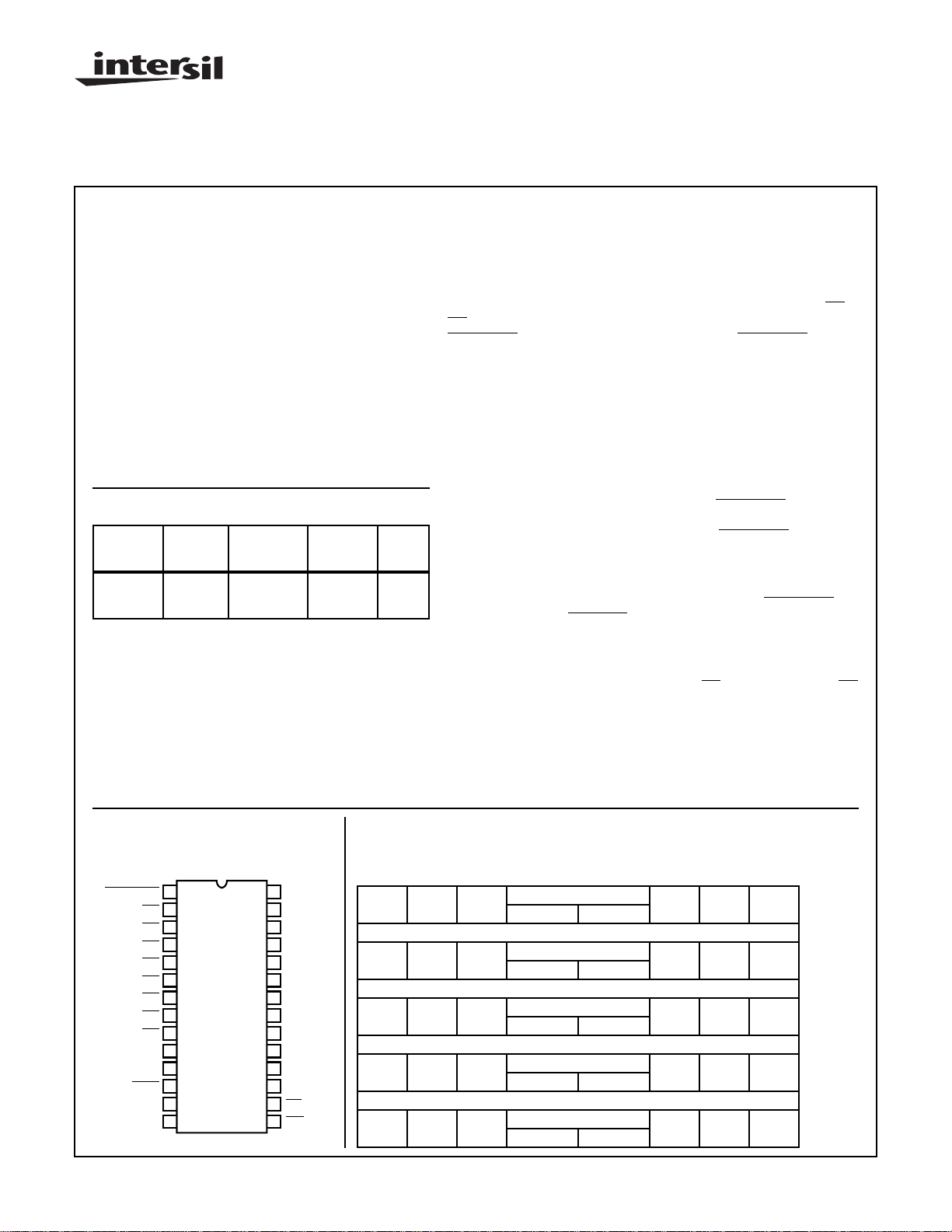
Ordering Information
TEMP.
PACKAGE
PDIP -40oC to
RANGE 5V 10V
CDP1877CE CDP1877E E28.6
+85oC
PKG.
NO.
Programmable Interrupt Controller (PIC)
Description
The CDP1877 and CDP1877C are programmable 8-level interrupt controllers designed for use in CDP1800 series microprocessor systems. They
provide added versatility by extending the number of permissible interrupts
from 1 to N in increments of 8.
When a high to low transition occurs on any of the PIC interrupt lines (
IR7), it will be latched and, unless the request is masked, it will cause the
INTERRUPT line on the PIC and consequently the INTERRUPT input on
the CPU to go low.
The CPU accesses the PIC by having interrupt vector register R(1) loaded
with the memory address of the PIC. After the interrupt S3 cycle, this register value will appear at the CPU address bus, causing the CPU to fetch an
instruction from the PIC. This fetch cycle clears the interrupt request latch
bit to accept a new high-to-low transition, and also causes the PIC to issue a
long branch instruction (CO) followed by the preprogr ammed v ector address
written into the PIC’s address registers, causing the CPU to branch to the
address corresponding to the highest priority active interrupt request.
If no other unmasked interrupts are pending, the
PIC will return high. When an interrupt is requested on a masked interrupt
line, it will be latched but it will not cause the PIC
low. All pending interrupts, masked and unmasked, will be indicated by a “1”
in the corresponding bit of the status register. Reading of the status register
will clear all pending interrupt request latches.
Several PICs can be cascaded together b y connecting the
put of one chip to the
vides 8 additional interrupt levels to the system. The number of units
cascadable depends on the amount of memory space and the extent of the
address decoding in the system.
Interrupts are prioritized in descending order;
has the lowest priority.
The CDP1877 and CDP1877C are functionally identical. They differ in that
the CDP1877 has a recommended operating voltage range of 4V to 10.5V,
and the CDP1877C has a recommended operating voltage range of 4V to
6.5V.
CASCADE input of another. Each cascaded PIC pro-
INTERRUPT output of the
INTERRUPT output to go
INTERRUPT out-
IR7 has the highest and IR0
IR0 to
Pinout
CDP1877, CDP1877C (PDIP)
TOP VIEW
V
CASCADE
CAUTION: These devices are sensitive to electrostatic discharge; follow proper IC Handling Procedures.
http://www.intersil.com or 407-727-9207
IR7
IR6
IR5
IR4
IR3
IR2
IR1
IR0
TPA
TPB
MWR
MRD
V
1
2
3
4
5
6
7
8
9
10
11
12
13
14
SS
28
DD
BUS 7
27
BUS 6
26
BUS 5
25
24
BUS 4
23
BUS 3
BUS 2
22
21
BUS 1
20
BUS 0
CS/Ax
19
18
CS/Ay
17
CS
16
CS
INT
15
| Copyright © Intersil Corporation 1999
Programming Model
PROGRAMMABLE INTERRUPT CONTROLLER (PIC)
BUS 7 BUS 0
PAGE REGISTER WRITE
A15 A14 A13 A12 A11 A10 A9 A8
BUS 7 BUS 0
CONTROL REGISTER WRITE
B7 B6 B5 B4 B3 B2 B1 B0
BUS 7 BUS 0
MASK REGISTER WRITE
M7 M6 M5 M4 M3 M2 M1 M0
BUS 7 BUS 0
STATUS REGISTER READ
S7 S6 S5 S4 S3 S2 S1 S0
BUS 7 BUS 0
POLLING REGISTER READ
P7 P6 P5 P4 P3 P2 P1 P0
4-82
File Number
ONLY
ONLY
ONLY
ONLY
ONLY
1319.2

CDP1877, CDP1877C
Absolute Maximum Ratings Thermal Information
DC Supply-Voltage Range, (VDD)
(All Voltages Referenced to VSSTerminal)
CDP1877. . . . . . . . . . . . . . . . . . . . . . . . . . . . . . . . . . -0.5V to +11V
CDP1877C . . . . . . . . . . . . . . . . . . . . . . . . . . . . . . . . . -0.5V to +7V
Input Voltage Range, All Inputs . . . . . . . . . . . . . -0.5V to VDD +0.5V
DC Input Current, Any One Input. . . . . . . . . . . . . . . . . . . . . . . . .±10mA
CAUTION: Stresses above those listed in “Absolute Maximum Ratings” may cause permanent damage to the device. This is a stress only rating and operation
of the device at these or any other conditions above those indicated in the operational sections of this specification is not implied.
Thermal Resistance (Typical) θJA (oC/W)
PDIP Package. . . . . . . . . . . . . . . . . . . . . . . . . . . . . 55
Device Dissipation Per Output Transistor
TA = Full Package Temperature Range
(All Package Types). . . . . . . . . . . . . . . . . . . . . . . . . . . . . . 100mW
Operating Temperature Range (TA)
Package Type E. . . . . . . . . . . . . . . . . . . . . . . . . . .-40oC to +85oC
Storage Temperature Range (T
) . . . . . . . . . . . .-65oC to +150oC
STG
Lead Temperature (During Soldering)
At distance 1/16 ± 1/32 In. (1.59 ± 0.79mm)
from case for 10s max. . . . . . . . . . . . . . . . . . . . . . . . . . . . +265oC
Static Electrical Specifications At T
= -40 to +85oC, VDD±5%, Unless Otherwise Specified
A
CONDITIONS LIMITS
CDP1877 CDP1877C
PARAMETER
Quiescent Device
Current
Output Low Drive (Sink)
Current
Output High Drive
(Source) Current
Output Voltage Low Level
(Note 2)
Output Voltage High Level
(Note 2)
Input Low Voltage V
V
O
(V)
I
DD
- 0, 5 5 - 0.01 50 - 0.02 200 µA
- 0, 10 10 - 1 200 - - - µA
I
OL
0.4 0, 5 5 1.6 3.2 - 1.6 3.2 - mA
0.5 0, 10 10 2.6 5.2 - - - - mA
I
OH
4.6 0, 5 5 -1.15 -2.3 - -1.15 -2.3 - mA
9.5 0, 10 10 -2.6 -5.2 - - - - mA
V
OL
- 0, 5 5 - 0 0.1 - 0 0.1 V
- 0, 10 10 - 0 0.1 - - - V
V
OH
- 0, 5 5 4.9 5 - 4.9 5 - V
- 0, 10 10 9.9 10 - - - - V
0.5, 4.5 - 5 - - 1.5 - - 1.5 V
IL
V
(V)
V
IN
(V)
DD
MIN
(NOTE1)
TYP MAX MIN
(NOTE1)
TYP MAX
0.5, 9.5 - 10 - - 3 - - - V
Input High Voltage V
0.5, 4.5 - 5 3.5 - - 3.5 - - V
IH
0.5, 9.5 - 10 7 - - - - - V
Input Leakage Current I
Three-State Output
Leakage Current
Operating Device Current
I
(Note 3)
Input Capacitance C
Output Capacitance C
IN
I
OUT
OPER
OUT
Any
Input
0, 5 5 - - ±1- - ±1 µA
0, 10 10 - - ±2- - -µA
0, 5 0, 5 5 - ±10
0, 10 0, 10 10 - ±10
- - 5 - 0.5 1.0 - 0.5 1.0 mA
- - 10 - 1.9 3.0 - - - mA
IN
- - - - 5 7.5 - 5 7.5 pF
- - - - 10 15 - 10 15 pF
-4
±1-±10
-4
±10 - - - µA
-4
±1 µA
NOTES:
1. Typical values are for TA = +25oC and nominal VDD.
2. IOL = IOH = 1µA
3. Operating current is measured under worst-case conditions in a 3.2MHz CDP1802A system, one PIC access per instruction cycle.
UNITS
4-83
CDP1877, CDP1877C
Operating Conditions At T
= Full package temperature range. F or maximum reliability, operating conditions should be selected so
A
that operation is always within the following ranges:
LIMITS
CDP1877 CDP1877C
PARAMETER
MIN MAX MIN MAX
DC Operating Voltage Range 4 10.5 4 6.5 V
Input Voltage Range V
TPA
CA/A
CA/A
CASC
CS
CS
4-BIT
X
Y
LATCH
READ
STATUS
REGISTER
TPB
MWR
MRD
WRITE
MASK
REGISTER
DECODER
CS
SS
V
DD
WRITE PAGE REGISTER
WRITE CONTROL REGISTER
WRITE MASK REGISTER
READ STATUS REGISTER
READ POLLING REGISTER
READ LONG BRANCH
INT
WRITE
PAGE
REGISTER
READ
LONG
BRANCH
V
SS
V
DD
UNITS
V
IR7
IR6
IR5
IR4
IR3
IR2
IR1
IR0
EN CLEAR
INTERRUPT
LATCH/
STATUS
REGISTER
CLEAR
EN
HIGH
VECTOR
ADDRESS
READ POLLING
REGISTER
LOW
VECTOR
ADDRESS
UPPER BITS
MASK
REGISTER
CLEAR
PRIORITY
ENCODER/
VECTOR
ADDRESS
GENERATION
INTERVAL
CONTROL REGISTER
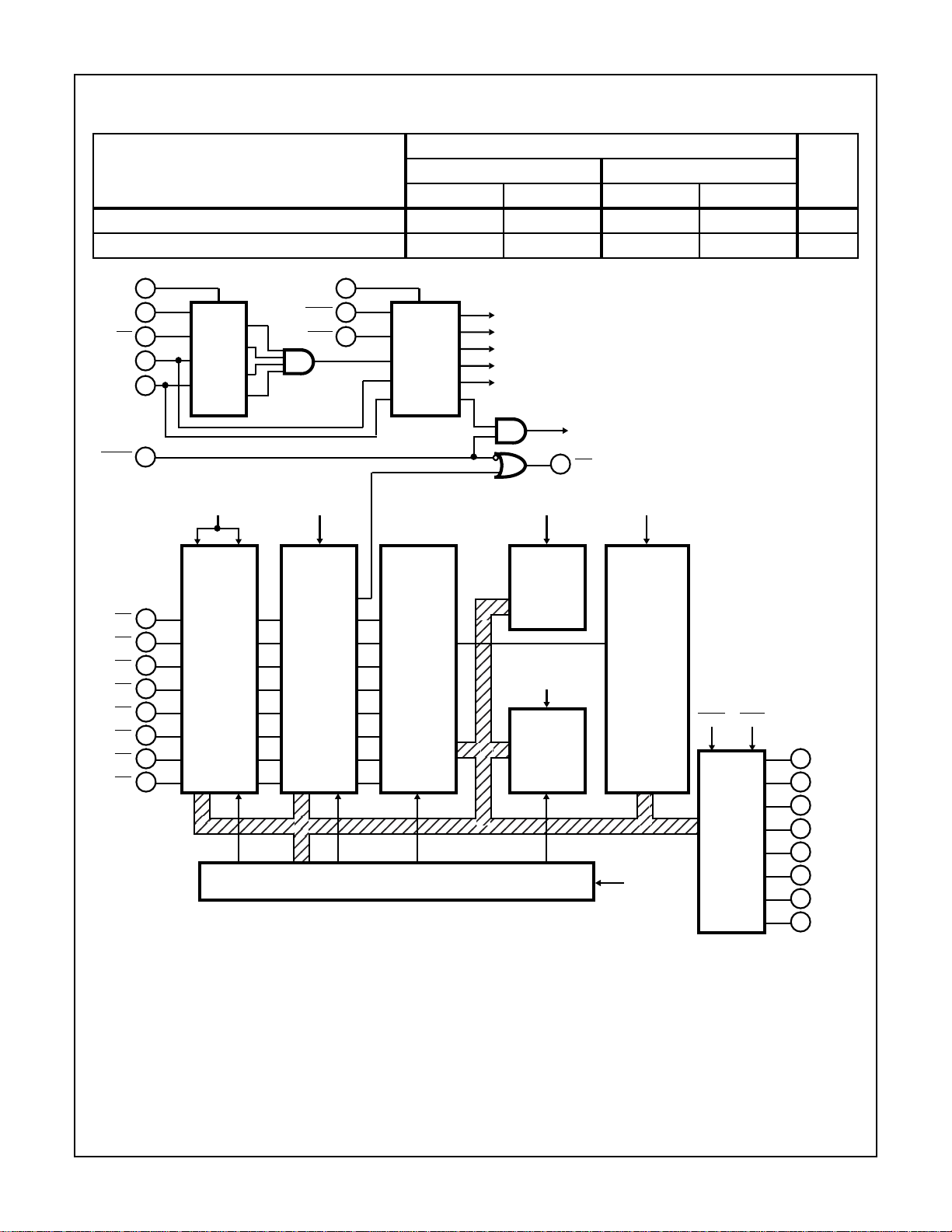
FIGURE 1. FUNCTIONAL DIAGRAM FOR CDP1877
EN
EN
LONG
BRANCH
INSTRUCTION
GENERATE
LOGIC
WRITE
CONTROL
REGISTER
MWR MRD
DAT A
BUS
BUFFERS
BUS 0
BUS 1
BUS 2
BUS 3
BUS 4
BUS 5
BUS 6
BUS 7
4-84

CDP1877, CDP1877C
Functional Definitions for CDP1877 and CDP1877C Terminals
TERMINAL USAGE TYPE
- V
V
DD
SS
BUS0 - BUS7 Data Bus - Communicates Information to and from CPU Bidirectional
IR0 - IR7 Interrupt Request Lines Input
INTERRUPT Interrupt to CPU Output
MRD, MWR Read/Write Controls from CPU Input
TPA, TPB Timing Pulses from CPU Input
CS Chip Selects, Enable Chip if Valid during TPA Input
CS,
, CS/A
CS/A
X
CASCADE Used for Cascading Several PIC Units. The INTERRUPT Output from a Higher
Power
Used as a Chip Select during TPA and as a Register Address During Read/Write Operations Input
Y
Priority PIC can be Tied to this Input, or the Input can be Tied to VDD if Cascading is Not Used.
Input
PIC Programming Model
INTERNAL REGISTERS
The PIC has three write-only programmable registers and
two read-only registers.
Page Register
This write only register contains the high order vector
address the device will issue in response to an interrupt
request. This high-order address will be the same for any of
the 8 possible interrupt requests; thus, interrupt vectoring differs only in location within a specified page.
BUS 7 BUS 0
PAGE REGISTER BITS
A15 A14 A13 A12 A11 A10 A9 A8
Control Register
The upper nibble of this write-only register contains the low
order vector address the device will issue in response to an
BUS 7 BUS 0
CONTROL REGISTER BITS
B7 B6 B5 B4 B3 B2 B1 B0
SETS UPPER BITS OF THE LOW ORDER VECTOR ADDRESS AS A
FUNCTION OF THE INTERVAL SELECT
interrupt request. The lower nibble is used for a master
interrupt reset, master mask reset and for interval select.
INTERVAL SELECT DETERMINES
NUMBER OF BYTES ALLOCATED TO
EACH INTERRUPT SERVICE ROUTINE
BIT 1 BIT 0 INTERVAL
00 2
01 4
10 8
1116
MASTER MASK RESET
0 RESETS ALL MASK REGISTER BITS
1 NO CHANGE
MASTER INTERRUPT RESET
0 RESETS ALL INTERRUPT LATCHES, CLEARS ANY
PENDING INTERRUPTS
1 NO CHANGE
WRITE ONLY
WRITE ONLY
4-85

CDP1877, CDP1877C
The Low Order Vector Address will be set according to the table below:
LOW ADDRESS BITS
INTERVAL SELECTED NO. OF BYTES
2 SETS A7 SETS A6 SETS A5 SET A4
4 SETS A7 SETS A6 SETS A5 X
8 SETS A7 SETS A6 X X
16 SETS A7 X X X
NOTES:
1. X = Don’t Care
2. All Don’t Care addresses and addresses A0-A3 are determined by interrupt request.
BIT B7 BIT B6 BIT B5 BIT B4
Mask Register
A ”1” written into any location in this write only register will
mask the corresponding interrupt request line. All interrupt
inputs (except
BUS 7 BUS 0
M7 M6 M5 M4 M3 M2 M1 M0
CASCADE) are maskable.
MASK REGISTER BITS
Status Register
In this read only register a “1” will be present in the
corresponding bit location for every masked or unmasked
pending interrupt.
WRITE ONLY
BUS 7 BUS 0
STATUS REGISTER BITS
S7 S6 S5 S4 S3 S2 S1 S0
Polling Register
This read only register provides the low order vector address
and is used to identify the source of interrupt if a polling
technique, rather than interrupt servicing, is used.
BUS 7 BUS 0
POLLING REGISTER BITS
P7 P6 P5 P4 P3 P2 P1 P0
RESPONSE TO INTERRUPT (AFTER S3 CYCLE)
The PIC’s response to interrogation by the CPU is always 3
bytes long, placed on the data bus in consecutive bytes in
the following format:
First (Instruction) Byte:
LONG BRANCH INSTRUCTION - CO (Hex)
BUS 7 BUS 0
11000000
READ ONLY
READ ONLY
4-86

CDP1877, CDP1877C
Second (High-Order Address) Byte
This byte is the High-Order vector Address that was written
into the PIC’s Page Register by the user. The PIC does not
alter this value in any way.
High-Order Vector Address
BUS 7 BUS 0
A15 A14 A13 A12 A11 A10 A9 A8
Third (Low-Order Address) Bytes
INTERVAL 2
BUS 7 BUS 0
A7 A6 A5 A4 0
INTERVAL 4
BUS 7 BUS 0
A7 A6 A5 00
INTERVAL 8
BUS 7 BUS 0
A7 A6 000
INTERVAL 16
BUS 7 BUS 0
A7 0000
Bits indicated by A
I2 I1 I0
Indicates active interrupt input number (binary 0 to 7).
(x = 4 to 7) are the same as pro-
X
I2 I1 I0
I2 I1 I0
I2 I1 I0
grammed into the control register. All other bits are
generated by the PIC.
REGISTER ADDRESSES
In order to read/write or obtain an interrupt vector from any
PIC in the system, all chip selects (CS/A
, CS/AY, CS, CS)
X
must be valid during TPA.
CS/A
and CS/AY are multiplexed addresses; both must be
X
high during TPA, and set according to this table during TPB
to access the proper register.
CS/A
X
1001READ Long Branch instruction and vector for highest
1010WRITE to Page Register
0110WRITE to Control Register
0001READ Status Register
0010WRITE to Mask Register
0101READ Polling Register (Used to identify INTERRUPT
1 1 X X Unused condition
CS/A
Y
RD WR ACTION TAKEN
priority unmasked interrupt pending.
source if Polling technique rather than INTERRUPT service is used.)
4-87

CDP1877, CDP1877C
PIC Application Examples
Example 1 - Single PIC Application
Figure 2 shows all the connections required between CPU
and PIC to handle eight levels of interrupt control.
MA7
MA6
MA5
MA4
CPU PIC
MWR
MRD
TPA
TPB
INT
BUS
FIGURE 2. PIC AND CPU CONNECTION DIAGRAM
Programming
Programming the PIC consists of the following steps:
1. Disable interrupt at CPU
2. Reset Master Interrupt Bit, B3, of Control Register.
3. Write a “1” into the Interrupt Input bit location of the Mask
Register, if masking is desired.
4. Write the High-Order Address byte into the Page
Register.
5. Write the Low-Order Address and the vector interval into
the Control Register.
6. Program R(1) of the CPU to point to the PIC so that the
Long Branch instruction can be read from the PIC during
the Interrupt Service routine.
CS/A
CS/A
CS
CS
X
Y
CASC V
DD
CDP1877CDP1802
MWR
MRD
TPA
TPB
INT
BUS
IR7
IR6
IR5
IR4
IR3
IR2
IR1
IR0
Values for Example 1 with LOCATION 84E0 arbitrarily chosen as the Vector Address with interval of eight bytes,
IR4
pending, is shown in Table 1.
In deriving the above addresses, all Don’t Care bits are
assumed to be 0.
When an INTERRUPT (
IR4) is received by the CPU, it will
address the PIC and will branch to the interrupt service
routine.
The three bytes generated by the PIC will be:
1st Byte = C0
2nd Byte = 84
3rd Byte = E0
H
H
H
TABLE 1. REGISTER ADDRESS VALUES
REGISTER REGISTER ADDRESS OPERATION DATA BYTE
MASK E000H WRITE 00
CONTROL E040H WRITE CE
PAGE E080H WRITE 84
STATUS E000H READ 10
POLLING E040H READ E0
R(1) (IN CPU) E080H - -
4-88
H
H
H
H
H

CDP1877, CDP1877C
Example 2 - Multi-PIC Application
Figure 3 shows all the connections required between CPU
and PIC’s to handle sixteen levels of interrupt control.
MA7
MA6
MA5
CPU
CDP1802
MA1
MA0
MWR
MRD
TPA
TPB
INT
BUS
CS/A
CS/A
CS
CS
MWR
MRD
TPA
TPB
INT
BUS
X
Y
PIC 1
CDP1877
CASC
IR7
IR6
IR5
IR4
IR3
IR2
IR1
IR0
+V
HIGHEST
PRIORITY
INTERRUPT
FIGURE 3. PICs AND CPU CONNECTION DIAGRAM
Register Address Assignments
The low-byte register address for any WRITE or READ
operation is the same as shown in Table 1.
The High-Byte register differs for each PIC because of the
linear addressing technique shown in the example:
PIC 1 = 111XXX01 (E1
PIC 2 = 111XXX10 (E2
for X = 0)
H
for X = 0)
H
The R(1) vector address is unchanged. This address will
select both PICs simultaneously (R(1). 1 = 111XXX00 =
E0
). Internal CDP1877 logic controls which PIC will
H
respond when an interrupt request is serviced.
Additional PIC Application Comments
The interval select options provide significant flexibility for
interrupt routine memory allocations:
• The 2-byte interval allows one to dedicate a full page to
interrupt servicing, with variable space between routines,
by specifying indirect vectoring with 2-byte short branch
instructions on the current page.
CS/A
CS/A
CS
CS
MWR
MRD
TPA
TPB
INT
BUS
X
Y
PIC 2
CDP1877
CASC
IR7
IR6
IR5
IR4
IR3
IR2
IR1
IR0
LOWEST
PRIORITY
INTERRUPT
• The 4-byte interval allows for a 3-byte long branch to any
location in memory where the interrupt service routine is
located. The branch can be preceded by a Save
Instruction to save previous contents of X and P on the
stack.
• The 8-byte and 16-byte intervals allow enough space to
perform a service routine without indirect vectoring. The
amount of interval memory can be increased even further
if all 8 INTERRUPTS are not required. Thus a 4-lev el interrupt system could use alternate
IR Inputs, and expand the
interval to 16 and 32 bytes, respectively.
• The 4 Chip Selects allow one to conserve total allotted
memory space to the PIC. For one chip, a total of 4
address lines could be used to select the device, mapping
it into as little as 4-K of memory space. Note that this
selection technique is the only one that allows the PIC to
work properly in the system: I/O mapping cannot be used
because the PIC must work within the CDP1800 interrupt
structure to define the vector address. Decoded signals
also will not work because the chip selects must be valid
on the trailing edge of TPA.
4-89
CDP1877, CDP1877C
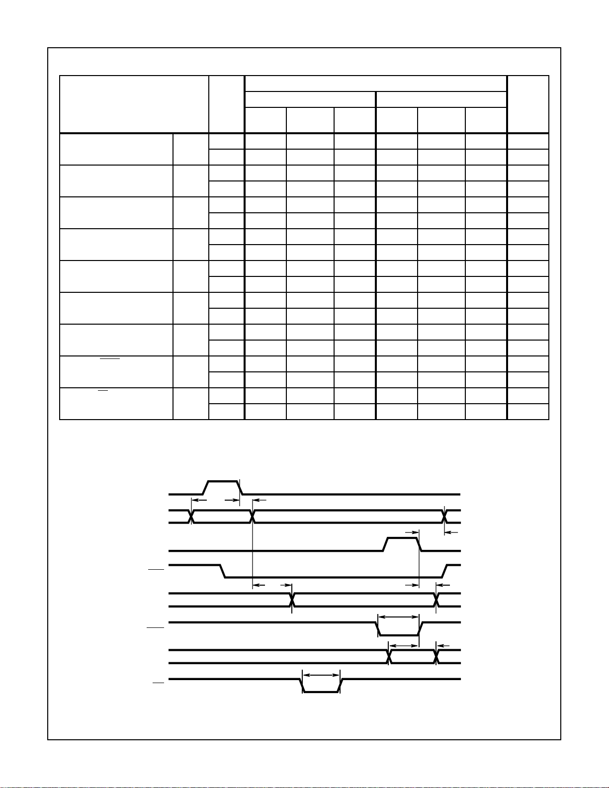
Dynamic Electrical Specifications At T
V
PARAMETER
Address to TPA Setup Time t
Address to TPA Hold Time t
Data Valid after TPB t
Data Hold Time from Write t
Address to Valid Data
AS
AH
DTPB
HW
t
DR
Access Time
Data Setup Time to Write t
Address Hold from TPB t
Minimum MWR Pulse Width t
Minimum IR Pulse Width t
DSU
HTPB
MWR
IRX
NOTE:
1. Typical values are for TA = 25oC and VDD±5%.
DD
(V)
560- -60- -ns
10 40 - - - - - ns
560- -60- -ns
10 40 - - - - - ns
5 370 - - 370 - - ns
10 210 310 - - - - ns
530- -30- -ns
10 40 - - - - - ns
5 - 340 490 - 340 490 ns
10 - 125 230 - - - ns
50 - - 0 - -ns
10 0 - - - - - ns
580- -80- -ns
10 40 - - - - - ns
5 130 - - 130 - - ns
10 60 - - - - - ns
5 130 - - 130 - - ns
10 60 - - - - - ns
= -40 to +85oC, VDD±5%, tR, tF = 20ns, VIH = 0.7VDD, VIL = 0.3VDD, CL = 50pF
A
LIMITS
CDP1877 CDP1877C
MIN
(NOTE 1)
TYP MAX MIN
(NOTE 1)
TYP MAX
UNITS
TPA
MEMORY ADDRESS
TPB
MRD
DATA FROM PIC TO BUS
MWR
DATA FROM BUS TO PIC
IRX
t
AS
HIGH BYTE LOW BYTE
t
AH
t
DR
VALID DATA
t
IRX
FIGURE 4. TIMING WAVEFORMS FOR CDP1877
4-90
t
MWR
t
DSU
VALID DATA
t
t
DH
t
DTPB
HTPB

CDP1877, CDP1877C
All Intersil semiconductor products are manufactured, assembled and tested under ISO9000 quality systems certification.
Intersil products are sold by description only. Intersil Corporation reserves the right to make changes in circuit design and/or specifications at any time without
notice. Accordingly, the reader is cautioned to verify that data sheets are current before placing orders. Information furnished by Intersil is believed to be accurate
and reliable. However, no responsibility is assumed by Intersil or its subsidiaries for its use; nor for any infringements of patents or other rights of third parties which
may result from its use. No license is granted by implication or otherwise under an y patent or patent rights of Intersil or its subsidiaries.
For information regarding Intersil Corporation and its products, see web site http://www.intersil.com
Sales Office Headquarters
NORTH AMERICA
Intersil Corporation
P. O. Box 883, Mail Stop 53-204
Melbourne, FL 32902
TEL: (407) 724-7000
FAX: (407) 724-7240
EUROPE
Intersil SA
Mercure Center
100, Rue de la Fusee
1130 Brussels, Belgium
TEL: (32) 2.724.2111
FAX: (32) 2.724.22.05
4-91
ASIA
Intersil (Taiwan) Ltd.
Taiwan Limited
7F-6, No. 101 Fu Hsing North Road
Taipei, Taiwan
Republic of China
TEL: (886) 2 2716 9310
FAX: (886) 2 2715 3029
 Loading...