

CDP1872C,
CDP1874C, CDP1875C
March 1997
Features
• Parallel 8-Bit Input/Output Register with Buffered Outputs
• High-Speed Data-In to Data-Out 85ns (Max) at V
• Flexible Applications In Microprocessor Systems as
Buffers and Latches
• High Order Address-Latch Capability in CDP1800Series Microprocessor Systems
• Output Sink Current = 5mA (Min) at V
DD
= 5V
• Three-State Output - CDP1872C and CDP1874C
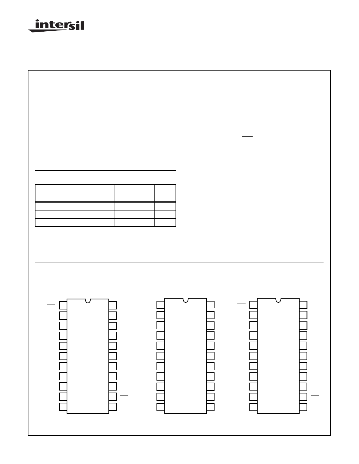
Ordering Information
PART
NUMBER TEMP. RANGE PACKAGE
CDP1872CE -40oC to +85oC PDIP E22.4
CDP1874CE -40oC to +85oC PDIP E22.4
CDP1875CE -40oC to +85oC PDIP E22.4
High-Speed 8-Bit Input and Output Ports
Description
The CDP1872C, CDP1874C and CDP1875C devices are
high-speed 8-bit parallel input and output ports designed for
DD
PKG.
= 5V
NO.
use in the CDP1800 microprocessor system and for general
use in other microprocessor systems. The CDP1872C and
CDP1874C are 8-bit input ports; the CDP1875C is an 8-bit
output port.
These devices have flexible capabilities as buffers and data
latches and are reset by
CLR input when the data strobe is
not active.
The CDP1872C and CDP1874C are functionally identical
except for device selects.The CDP1872C has one active low
and one active high select; the CDP1874C has two active
high device selects. These devices also feature Three-state
outputs when deselected. Data is strobed into the register on
the leading edge of the CLOCK and latched on the trailing
edge of the CLOCK.
The CDP1875C is an output port with data latched into the
registers when the device selects are active. There are two
active high and one active low selects. The output buffers
are enabled at all times.
Pinouts
CS1
DI0
DO0
DI1
D01
DI2
D02
DI3
D03
CLOCK
V
SS
CDP1872C INPUT PORT
(PDIP)
TOP VIEW
1
2
3
4
5
6
7
8
9
10
11
CDP1874C INPUT PORT
(PDIP)
TOP VIEW
22
V
DD
21
DI7
20
D07
19
DI6
18
D06
17
DI5
16
D05
15
DI4
14
D04
13
CLR
12
CS2
CLOCK
CS1
DI0
DO0
DI1
D01
DI2
D02
DI3
D03
V
1
2
3
4
5
6
7
8
9
10
11
SS
22
V
DD
21
DI7
20
D07
19
DI6
18
D06
17
DI5
16
D05
15
DI4
14
D04
13
CLR
12
CS2
CDP1875C OUTPUT PORT
(PDIP)
TOP VIEW
1
CS1
2
DI0
3
DO0
4
DI1
5
D01
6
DI2
7
D02
8
DI3
9
D03
10
CS3
11
V
SS
22
V
DD
21
DI7
20
D07
19
DI6
18
D06
17
DI5
16
D05
15
DI4
14
D04
13
CLR
12
CS2
CAUTION: These devices are sensitive to electrostatic discharge; follow proper IC Handling Procedures.
http://www.intersil.com or 407-727-9207
| Copyright © Intersil Corporation 1999
4-76
File Number
1255.2
CDP1872C, CDP1874C, CDP1875CCDP1872C, CDP1874C, CDP1875C
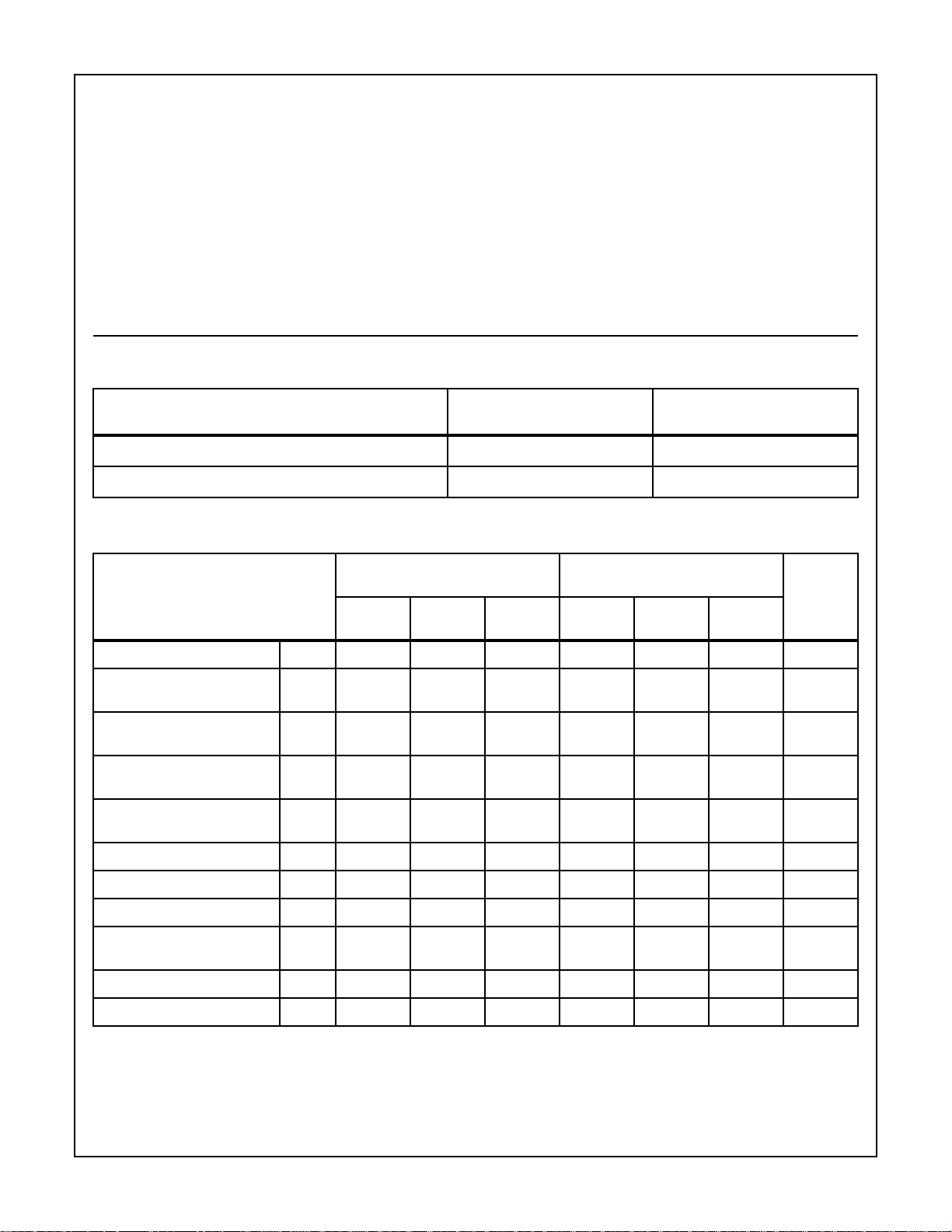
Absolute Maximum Ratings Thermal Information
DC Supply Voltage Range, (VDD). . . . . . . . . . . . . . . . . -0.5V to +7V
(Voltage referenced to VSS Terminal)
Input Voltage Range, All Inputs . . . . . . . . . . . . . -0.5V to VDD +0.5V
DC Input Current, Any One Input. . . . . . . . . . . . . . . . . . . . . . . . .±10mA
CAUTION: Stresses above those listed in “Absolute Maximum Ratings” may cause permanent damage to the device. This is a stress only rating and operation
of the device at these or any other conditions above those indicated in the operational sections of this specification is not implied.
Thermal Resistance (Typical) θJA (oC/W)
PDIP Package. . . . . . . . . . . . . . . . . . . . . . . . . . . . . 75
Device Dissipation Per Output Transistor
TA = Full Package Temperature Range
(All Package Types). . . . . . . . . . . . . . . . . . . . . . . . . . . . . . 100mW
Operating Temperature Range (TA)
Package Type E. . . . . . . . . . . . . . . . . . . . . . . . . . .-40oC to +85oC
Storage Temperature Range (T
) . . . . . . . . . . . .-65oC to +150oC
STG
Lead Temperature (During Soldering)
At distance 1/16 ± 1/32 In. (1.59 ± 0.79mm)
from case for 10s max. . . . . . . . . . . . . . . . . . . . . . . . . . . . +265oC
Recommended Operating Conditions At T
= -40 to +85oC. For maximum reliability, operating conditions should be selected
A
so that operation is always within the following ranges:
LIMITS
PARAMETER
ALL TYPES UNITS
DC Operating-Voltage Range 4 to 6.5 V
Input Voltage Range VSS to V
Static Electrical Specifications At T
= -40 to +85oC, VDD±5%, Unless Otherwise Specified.
A
DD
LIMITS
PARAMETER
Quiescent Device Current I
Output Low Drive (Sink)
TEST CONDITIONS
V
O
(V)
DD
I
OL
-0, 55 - 2550µA
0.4 0, 5 5 5 10 - mA
V
(V)
IN
V
DD
(V) MIN
ALL TYPES
(NOTE 1)
TYP MAX
Current
Output High Drive (Source)
I
OH
4.6 0, 5 5 -4 -7 - mA
Current
Output Voltage Low-Level
V
OL
- 0, 5 5 - 0 0.1 V
(Note 2)
V
UNITS
Output Voltage High-Level
V
OH
- 0, 5 5 4.9 5 - V
(Note 2)
Input Low Voltage V
Input High Voltage V
Input Leakage Current I
Three-State Output Leakage
I
OUT
IN
0.5, 4.5 - 5 - - 1.5 V
IL
0.5, 4.5 - 5 3.5 - - V
IH
- 0, 5 5 - - ±1 µA
0, 5 0, 5 5 - - ±5 µA
Current (Note 3)
Input Capacitance C
Output Capacitance (Note 3) C
IN
OUT
----15-pF
----15-pF
NOTES:
1. Typical values are for TA = +25oC and nominal VDD±5%.
2. IOL = IOH = 1µA
3. For CDP1872C and CDP1874C only.
4-77

Logic Diagrams
CS1
CS2
DI
CLOCK
CDP1872C, CDP1874C, CDP1875C
CS1
D
CRQ
DO
CS2
DI
CLOCK
D
CRQ
DO
CLR
FIGURE 1. EQUIVALENT LOGIC DIAGRAM (1 OF 8 LATCHES
SHOWN) FOR CDP1872C
CS1
CS2
CS3
CLR
DI
FIGURE 3. EQUIVALENT LOGIC DIAGRAM (1 OF 8 LATCHES SHOWN) FOR CDP1875C
Dynamic Electrical Specifications At T
= 25oC, VDD 5V, tR, tF = 10ns, VIH = 0.7VDD, VIL = 0.3VDD, CL = 150pF
A
PARAMETER
INPUT PORT (FIGURE 4)
Output Enable t
Output Disable t
Clock to Data Out t
Clear to Output t
Data In to Data Out t
Minimum Data Setup Time t
Data Hold Time t
Minimum Clock Pulse Width t
Minimum Clear Pulse Width t
NOTES:
1. Typical values are for TA = +25oC and VDD±5%.
2. Maximum values are for TA = +85oC and VDD±5%
CLR
FIGURE 2. EQUIVALENT LOGIC DIAGRAM (1 OF 8 LATCHES
SHOWN) for CDP1874C
D
C
Q
R
DO
LIMITS
CDP1872C, CDP1874C
EN
DIS
CLO
CRO
DIO
DSU
DH
CL
CR
(NOTE 1)
MIN
TYP
-4590 ns
-4590 ns
-4590 ns
- 80 160 ns
-5085 ns
-1030 ns
-1030 ns
-3060 ns
-3060 ns
(NOTE 2)
MAX
UNITS
4-78

CSI • CS2
(CDP1872C)
CSI • CS2
(CDP1874C)
CDP1872C, CDP1874C, CDP1875C
t
DSU
t
DH
CLOCK
DATA IN
t
EN
DATA BUS
(HIGH Z)
t
DIO
CLR
FIGURE 4. TIMING WAVEFORMS FOR CDP1872C AND CDP1874C (INPUT-PORT TYPES)
Dynamic Electrical Specifications At T
= 25oC, VDD 5V, tR, tF = 10ns, VIH = 0.7VDD, VIL = 0.3VDD, CL = 150pF
A
PARAMETER
OUTPUT PORT (FIGURE 5)
Clock to Data Out t
Clear to Output t
Data In to Data Out t
Minimum Data Setup Time t
Data Hold Time t
Minimum Clear Pulse Width t
NOTES:
1. Typical values are for TA = +25oC and VDD±5%.
2. Maximum values are for TA = +85oC and VDD±5%
CLO
CRO
DIO
DS
DH
CR
t
CL
t
CLO
t
CRO
t
CR
t
DIS
LIMITS
CDP1875C
MIN
(NOTE 1)
TYP
(NOTE 2)
MAX
UNITS
- 50 100 ns
- 80 160 ns
-5085 ns
-1030 ns
-1030 ns
-3060 ns
CSI • CS2 • CS3 = CLOCK
DATA IN
DATA OUT
CLR
t
CLO
t
DS
t
DIO
t
DH
FIGURE 5. TIMING WAVEFORMS FOR CDP1875C (OUTPUT PORT)
4-79
t
CRO
t
CR

CDP1872C, CDP1874C, CDP1875C
CLOCK
CDP1874C
DI
DATA IN
MRD
CDP1802
TPA
MA8
MA15
•
•
•
ADDRESS BUS
CLOCK
CDP1874C
CSI
CS2
D0
D1
D2
D3
D4
D5
D6
D7
CSI
DO
CS2
CS2
CS3
CDP1875C
V
DATA BUS
0 - 7
TPB
DATA BUS
DD
DI
CS1
DO
DATA OUT
FIGURE 6. CDP1874C USED AS AN INPUT PORT AND ADDRESS LATCH WITH CDP1875C USED AS AN OUTPUT PORT
D0 - D7
MRD
CDP1802A
CS2
DATA BUS
CLOCK
CDP1872C
N0
N1
N2
A0
A1
A2
CD74HC138
Y1
Y2
Y3
Y4
Y5
Y6
Y7
CS1
CS2
CS1
CLOCK
CDP1872C
DATA BUS
FIGURE 7. CDP1872C USED AS AN INPUT PORT AND SELECTED BY CD74HC138
DATA IN
DATA OUT
4-80

CDP1872C, CDP1874C, CDP1875CCDP1872C, CDP1874C, CDP1875C
MRD
CDP1802
DATA IN
DATA IN
DO - D7
MEMORY
TPB
TPB
CS2
CS3
DI
CDP1875C
CS2
DI
CDP1875C
CS3
CS1
DO
CS1
DO
DI
CDP1874C
DI
CDP1874C
CS1
CS1
N0 N1 N2
CS2
DO
CS2
DO
FIGURE 8. CDP1874C AND CDP1875C USED AS INPUT/OUTPUT BUFFERS
DATA OUT
DATA OUT
All Intersil semiconductor products are manufactured, assembled and tested under ISO9000 quality systems certification.
Intersil products are sold by description only. Intersil Corporation reserves the right to make changes in circuit design and/or specifications at any time without
notice. Accordingly, the reader is cautioned to verify that data sheets are current before placing orders. Information furnished by Intersil is believed to be accurate
and reliable. However, no responsibility is assumed b y Intersil or its subsidiaries for its use; nor for any infringements of patents or other rights of third parties which
may result from its use. No license is granted by implication or otherwise under an y patent or patent rights of Intersil or its subsidiaries.
For information regarding Intersil Corporation and its products, see web site http://www.intersil.com
Sales Office Headquarters
NORTH AMERICA
Intersil Corporation
P. O. Box 883, Mail Stop 53-204
Melbourne, FL 32902
TEL: (407) 724-7000
FAX: (407) 724-7240
EUROPE
Intersil SA
Mercure Center
100, Rue de la Fusee
1130 Brussels, Belgium
TEL: (32) 2.724.2111
FAX: (32) 2.724.22.05
4-81
ASIA
Intersil (Taiwan) Ltd.
Taiwan Limited
7F-6, No. 101 Fu Hsing North Road
Taipei, Taiwan
Republic of China
TEL: (886) 2 2716 9310
FAX: (886) 2 2715 3029
 Loading...