March 1997
CDP1854A/3,
CDP1854AC/3
High Reliability CMOS Programmable Universal
Asynchronous Receiver/Transmitter (UART)
Features
• Two Operating Modes
- Mode 0 - Functionally Compatible with Industry
Types Such as the TR1602A and CDP6402
- Mode 1 - Interfaces Directly with CDP1800 Series
Microprocessors without Additional Components
• Full or Half-Duplex Operation
• Parity, Framing, and Overrun Error Detection
• Fully Programmable with Externally Selectable Word
Length (5-8 Bits), Parity Inhibit, Even/Odd Parity, and
1, 1-1/2, or 2 Stop Bits
Ordering Information
PACK-
AGE
SBDIP -55oC to +125oC CDP1854ACD3 CDP1854ACD3 D40.6
TEMP.
RANGE
5V/200K
BAUD
10V/400K
BAUD
PKG.
NO.
Description
The CDP1854A/3 and CDP1854AC/3 are high reliability
silicon gate CMOS Universal Asynchronous Receiver/Transmitter (UART) circuits. They are designed to provide the
necessary formatting and control for interfacing between
serial and parallel data. For example, these UARTs can be
used to interface between a peripheral or terminal with serial
I/O ports and the 8-bit CDP1800-series microprocessor
parallel data bus system. The CDP1854A/3 is capable of full
duplex operation, i.e., simultaneous conversion of serial
input data to parallel output data and parallel input data to
serial output data.
The CDP1854A/3 UART can be programmed to operate in
one of two modes by using the mode control input. When the
mode input is high (MODE = 1), the CDP1854A/3 is directly
compatible with the CDP1800 series microprocessor system
without additional interface circuitry. When the mode input is
low (MODE = 0), the device is functionally compatible with
industry standard UARTs such as the TR1602A and
CDP6402. It is also pin compatible with these types, except
that pin 2 is used for the mode control input.
The CDP1854A/3 and the CDP1854AC/3 are functionally
identical. The CDP1854A/3 has a recommended operating
voltage range of 4V to 10.5V, and the CDP1854AC/3 has a
recommended operating voltage range of 4V to 6.5V.
Pinouts
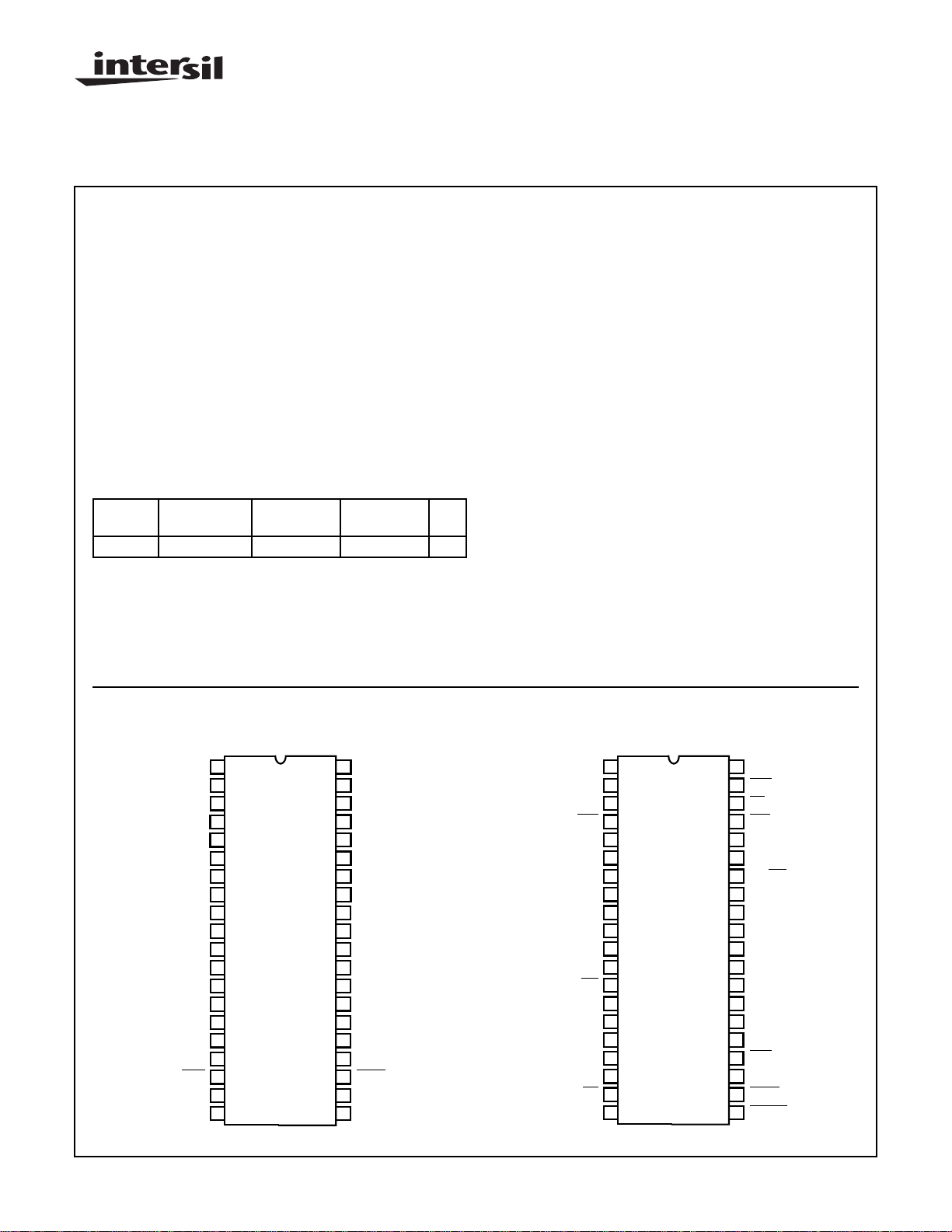
CDP1854A/3, CDP1854AC/3 (SBDIP) (MODE 0)
MODE (V
VDD
SS
V
SS
RRD
R BUS 7
R BUS 6
R BUS 5
R BUS 4
R BUS 3
R BUS 2
R BUS 1
R BUS 0
PE
FE
OE
SFD
R CLOCK
DAR
DA
SDI
CDP1854A/3, CDP1854AC/3 (SBDIP) (MODE 1)
TOP VIEW
1
2
)
3
4
5
6
7
8
9
10
11
12
13
14
15
16
17
18
19
20
40
39
38
37
36
35
34
33
32
31
30
29
28
27
26
25
24
23
22
21
T CLOCK
EPE
WLS 1
WLS 2
SBS
PI
CRL
T BUS 7
T BUS 6
T BUS 5
T BUS 4
T BUS 3
T BUS 2
T BUS 1
T BUS 0
SD0
TSRE
THRL
THRE
MR
V
MODE (VDD)
DD
V
SS
CS2
R BUS 7
R BUS 6
R BUS 5
R BUS 4
R BUS 3
R BUS 2
R BUS 1
R BUS 0
INT
FE
PE/OE
RSEL
R CLOCK
TPB
DA
SDI
TOP VIEW
1
2
3
4
5
6
7
8
9
10
11
12
13
14
15
16
17
18
19
20
NC = NO CONNECT
40
39
38
37
36
35
34
33
32
31
30
29
28
27
26
25
24
23
22
21
T CLOCK
CTS
ES
PS1
NC
CS3
RD/
WR
T BUS 7
T BUS 6
T BUS 5
T BUS 4
T BUS 3
T BUS 2
T BUS 1
T BUS 0
SD0
RTS
CS1
THRE
CLEAR
CAUTION: These devices are sensitive to electrostatic discharge; follow proper IC Handling Procedures.
http://www.intersil.com or 407-727-9207
| Copyright © Intersil Corporation 1999
5-62
File Number 1715.2

CDP1854A/3, CDP1854AC/3
Absolute Maximum Ratings Thermal Information
DC Supply-Voltage Range, (VDD)
(All voltages referenced to VSS terminal)
CDP1854A/3. . . . . . . . . . . . . . . . . . . . . . . . . . . . . . . .-0.5 to +11V
CDP1854AC/3 . . . . . . . . . . . . . . . . . . . . . . . . . . . . . . .-0.5 to +7V
Input Voltage Range, All Inputs . . . . . . . . . . . . . . -0.5 to VDD +0.5V
DC Input Current, Any One Input. . . . . . . . . . . . . . . . . . . . . . . . .±10mA
Device Dissipation Per Output Transistor
For TA = Full Package-Temperature Range . . . . . . . . . . . 100mW
Operating-Temperature Range (TA)
Package Type D. . . . . . . . . . . . . . . . . . . . . . . . . . . . .-55oC to +125oC
CAUTION: Stresses above those listed in “Absolute Maxim um Ratings” ma y cause permanent damage to the device . This is a stress only rating and oper ation of
the device at these or any other conditions above those indicated in the operational sections of this specification is not implied.
NOTE:
1. θJA is measured with the component mounted on an evaluation PC board in free air.
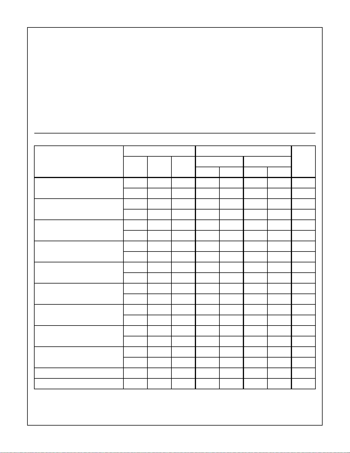
Static Electrical Specifications
CONDITIONS LIMITS
Thermal Resistance (Typical, Note 1) θJA (oC/W) θJC (oC/W)
SBDIP Package. . . . . . . . . . . . . . . . . . 55 15
Maximum Junction Temperature . . . . . . . . . . . . . . . . . . . . . . +150oC
Maximum Storage Temperature Range (T
) . . .-65oC to +150oC
STG
Maximum Lead Temperature (Soldering 10s)
At Distance 1/16 ±1/32 inch (1.59 ±0.79mm) . . . . . . . . . . +265oC
PARAMETER
Quiescent Device Current I
Output Low Drive
(Sink) Current
Output High Drive
(Source) Current
Output Voltage Low-Level
(Note 1)
Output Voltage
High Level (Note 1)
Input Low Voltage V
Input High Voltage V
-55oC, +25oC +125oC
DD
V
O
(V)
- 0, 5 5 - 500 - 1000 µA
V
(V)
IN
V
(V)
DD
MIN MAX MIN MAX
UNITS
- 0, 10 10 - 500 - 1000 µA
I
OL
0.4 0, 5 5 0.75 - 0.5 - mA
0.5 0, 10 10 1.80 - 1.2 - mA
I
OH
4.6 0, 5 5 - -0.5 - -0.35 mA
9.5 0, 10 10 - -1.0 - -0.70 mA
V
OL
- 0, 5 5 - 0.1 - 0.2 V
- 0, 10 10 - 0.1 - 0.2 V
V
OH
- 0, 5 5 4.9 - 4.9 - V
- 0, 10 10 9.9 - 9.8 - V
0.5, 4.5 - 5 - 1.5 - 1.5 V
IL
0.5, 9.5 - 10 - 3 - 3 V
0.5, 4.5 - 5 3.5 - 3.5 - V
IH
0.5, 9.5 - 10 7 - 7 - V
Input Leakage Current I
Three-State Output
Leakage Current
Input Capacitance (Note 1) C
Output Capacitance (Note 1) C
NOTE:
1. Guaranteed but not tested.
I
OUT
IN
IN
OUT
- 0, 5 5 - ±1-±5 µA
- 0, 10 10 - ±1-±5 µA
0, 5 0, 5 5 - ±1-±10 µA
0, 10 0, 10 10 - ±1-±10 µA
----10-10pF
----15-15pF
5-63

Specifications CDP1854A/3, CDP1854AC/3
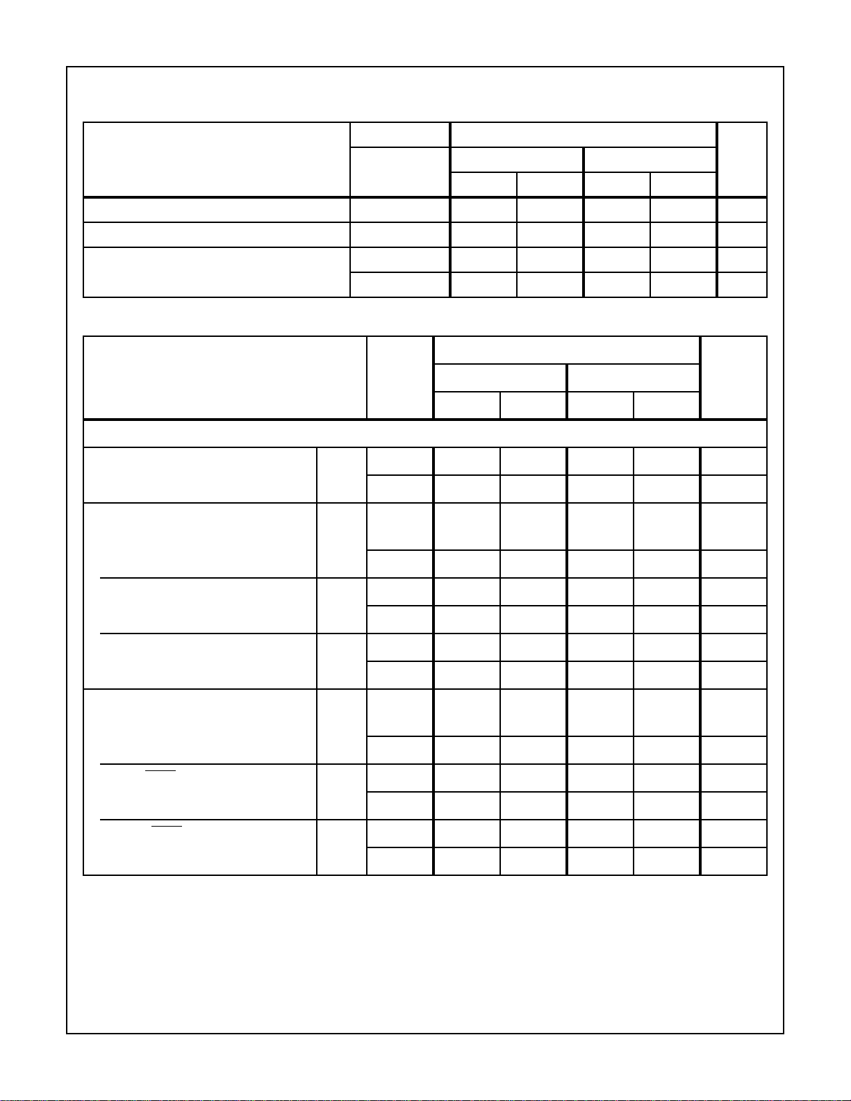
Operating Conditions At T
= Full Package-Temperature Range. For maximum reliability, operating conditions should be selected so
A
that operation is always within the following ranges:
CONDITIONS LIMITS
-55oC, +25oC +125oC
V
PARAMETER
(V)
DD
MIN MAX MIN MAX
UNITS
DC Operating Voltage Range - 4 10.5 4 6.5 V
Input Voltage Range - V
SS
V
DD
V
SS
V
DD
Baud Rate (Receive or Transmit) 5 - 250 - 215 K bits/s
10 - 520 - 430 K bits/s
Dynamic Electrical Specifications t
, tF = 15ns, VIH = VDD, VIL = VSS, CL = 100pF, (See Figure 1)
R
LIMITS
-55oC, +25oC +125oC
V
PARAMETER
(V)
DD
MIN MAX MIN MAX
UNITS
TRANSMITTER TIMING - MODE 1
Clock Period t
CC
5 240 - 280 - ns
10 120 - 145 - ns
V
Pulse Width t
CL
Clock Low Level 5 105 - 125 - ns
10 55 - 65 - ns
Clock High Level t
CH
5 135 - 155 - ns
10 65 - 80 - ns
TPB t
TT
5 125 - 165 - ns
10 70 - 80 - ns
Propagation Delay Time t
CD
Clock to Data Start Bit 5 - 425 - 485 ns
10 - 205 - 235 ns
TPB to THRE t
TTH
5 - 315 - 380 ns
10 - 155 - 185 ns
Clock to THRE t
CTH
5 - 335 - 390 ns
10 - 160 - 190 ns
5-64

CDP1854A/3, CDP1854AC/3
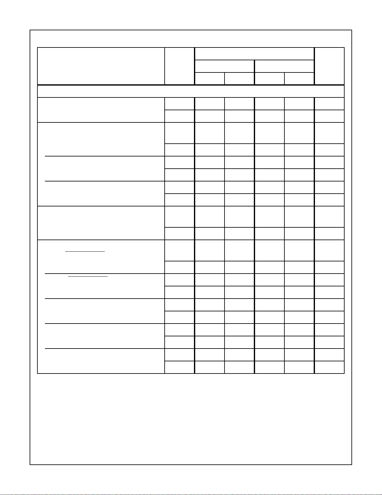
Dynamic Electrical Specifications t
PARAMETER
RECEIVER TIMING - MODE 1
Clock Period t
Pulse Width
Clock Low Level t
Clock High Level t
TPB t
Setup Time
Data Start Bit to Clock t
, tF = 15ns, VIH = VDD, VIL = VSS, CL = 100pF, (See Figure 2)
R
LIMITS
-55oC, +25oC +125oC
V
DD
CC
(V)
5 240 - 280 - ns
MIN MAX MIN MAX
10 120 - 145 - ns
CL
5 105 - 125 - ns
10 55 - 65 - ns
CH
5 135 - 155 - ns
10 65 - 80 - ns
TT
5 125 - 165 - ns
10 70 - 80 - ns
DC
5 105 - 120 - ns
UNITS
Propagation Delay Time
TPB to DATA AVAILABLE t
Clock to DATA AVAILABLE t
Clock to Overrun Error t
Clock to Parity Error t
Clock to Framing Error t
TDA
CDA
COE
CPE
CFE
10 65 - 70 - ns
5 - 295 - 340 ns
10 - 150 - 170 ns
5 - 305 - 355 ns
10 - 150 - 170 ns
5 - 305 - 330 ns
10 - 150 - 175 ns
5 - 305 - 330 ns
10 - 150 - 175 ns
5 - 280 - 330 ns
10 - 145 - 165 ns
5-65
 Loading...