Intersil Corporation CDP1853C, CDP1853 Datasheet

CDP1853,
CDP1853C
March 1997
Features
• Provides Direct Control of Up to 7 Input and 7 Output
Devices
• CHIP ENABLE (CE) Allows Easy Expansion for Multilevel I/O Systems
Ordering Information
PACKAGE TEMP. RANGE 5V 10V
PDIP -40oC to +85oC CDP1853CE CDP1853E E16.3
Burn-In CDP1853CEX - E16.3
SBDIP -40oC to +85oC CDP1853CD CDP1853D D16.3
Burn-In CDP1853CDX - D16.3
PKG.
NO.
N-Bit 1 of 8 Decoder
Description
The CDP1853 and CDP1853C are 1 of 8 decoders designed for
use in general purpose microprocessor systems. These
devices, which are functionally identical, are specifically
designed for use as gated N-bit decoders and interface directly
with the 1800-series microprocessors without additional components. The CDP1853 has a recommended operating voltage
range of 4V to 10.5V, and the CDP1853C has a recommended
operating voltage range of 4V to 6.5V.
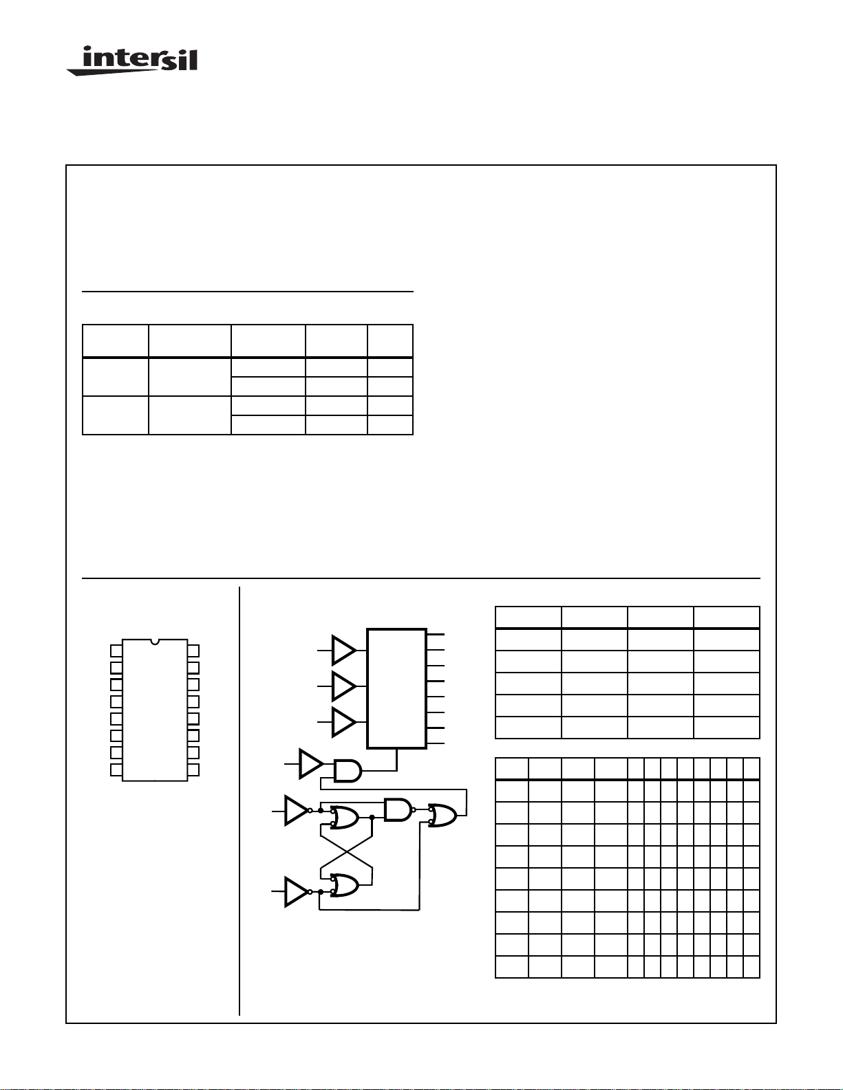
When CHIP ENABLE (CE) is high, the selected output will be
true (high) from the trailing edge of CLOCK A (high-to-low transition) to the trailing edge of CLOCK B (high-to-low transition).
All outputs will be low when the device is not selected (CE = 0)
and during conditions of CLOCK A and CLOCK B as shown in
Figure 2. The CDP1853 inputs N0, N1, N2, CLOCK A, and
CLOCK B are connected to an 1800-series microprocessor outputs N0, N1, N2, TPA, and TPB respectively, when used to
decode I/O commands as shown in Figure 5. The CHIP
ENABLE (CE) input provides the capability for multiple levels of
decoding as shown in Figure 6.
The CDP1853 can also be used as a general 1 of 8 decoder for
I/O and memory system applications as shown in Figure 4.
The CDP1853 and CDP1853C are supplied in hermetic 16-lead
dual-in-line ceramic (D suffix) and plastic (E suffix) packages.
Pinout
1
CLK A
2
N0
3
N1
4
OUT 0
5
OUT 1
6
OUT 2
7
OUT 3
8
V
SS
16 LEAD DIP
TOP VIEW
16
15
14
13
12
11
10
9
V
DD
CLK B
N2
CE
OUT 4
OUT 5
OUT 6
OUT 7
CDP1853 Functional Diagram
4
12
11
10
5
6
7
9
OUT 0
OUT 1
OUT 2
OUT 3
OUT 4
OUT 5
OUT 6
OUT 7
CE
CLOCK
A
(TPA)
CLOCK
B
(TPB)
2
N0
3
N1
14
N2
13
1
15
FIGURE 1.
1 OF 8
DECODER
EN
Qn
TRUTH TABLE
CE CL A CL B EN
1 0 0 Qn-1†
1011
1100
1111
0XX0
N2 N1 N0 EN 01234567
000110000000
001101000000
010100100000
011100010000
100100001000
101100000100
110100000010
111100000001
X X X 0 00000000
1 = High level, 0 = Low level, X = Don’t care
† Qn-1 = Enable remains in previous state.
CAUTION: These devices are sensitive to electrostatic discharge; follow proper IC Handling Procedures.
http://www.intersil.com or 407-727-9207
| Copyright © Intersil Corporation 1999
4-35
File Number
1189.2

CDP1853, CDP1853C
Absolute Maximum Ratings Thermal Information
DC Supply Voltage Range, (VDD)
(All voltage values referenced to VSS terminal)
CDP1853 . . . . . . . . . . . . . . . . . . . . . . . . . . . . . . . . -0.5V to +11V
CDP1853C. . . . . . . . . . . . . . . . . . . . . . . . . . . . . . . . -0.5V to +7V
Input Voltage Range, All Inputs . . . . . . . . . . . . . -0.5V to VDD +0.5V
DC Input Current, any One Input. . . . . . . . . . . . . . . . . . . . . . . . .±10mA
CAUTION: Stresses above those listed in “Absolute Maximum Ratings” may cause permanent damage to the device. This is a stress only rating and operation
of the device at these or any other conditions above those indicated in the operational sections of this specification is not implied.
Thermal Resistance (Typical) θJA (oC/W) θJC (oC/W)
PDIP Package. . . . . . . . . . . . . . . . . . . 85 N/A
SBDIP Package. . . . . . . . . . . . . . . . . . 85 22
Operating Temperature Range (TA)
Ceramic Packages (D Suffix Types) . . . . . . . . . . -55oC to +125oC
Plastic Packages (E Suffix Types). . . . . . . . . . . . . -40oC to +85oC
Storage Temperature Range (T
) . . . . . . . . . . . .-65oC to +150oC
STG
Lead Temperature (During Soldering). . . . . . . . . . . . . . . . . . +265oC
At distance 1/16 ± 1/32 In. (1.59 ± 0.79mm)
from case for 10s max
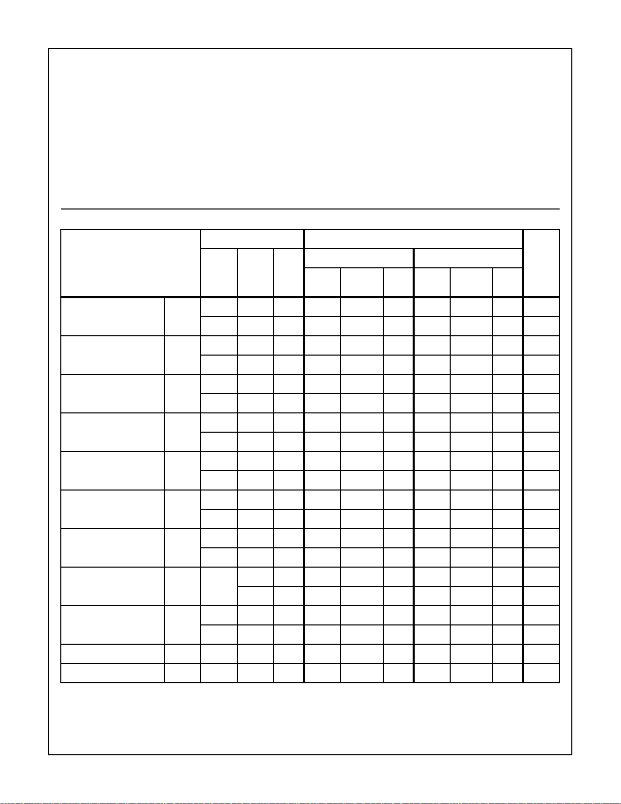
Static Electrical Specifications At T
V
PARAMETER
Quiescent Device
Current
Output Low Drive (Sink)
Current
Output High Drive
(Source) Current
Output Voltage Low Level
(Note 2)
Output Voltage High Level V
Input Low Voltage V
I
L
I
OL
I
OH
V
OL
OH
IL
(V)
- -5- 110- 550µA
- - 10 - 10 100 - - - µA
0.4 0, 5 5 1.6 3.2 - 1.6 3.2 - mA
0.5 0, 10 10 2.6 5.2 - - - - mA
4.6 0, 5 5 -1.15 -2.3 - -1.15 -2.3 - mA
9.5 0, 10 10 -2.6 -5.2 - - - - mA
- 0, 5 5 - 0 0.1 - 0 0.1 V
- 0, 10 10 - 0 0.1 - - - V
- 0, 5 5 4.9 5 - 4.9 5 - V
- 0, 10 10 9.9 10 - - - - V
0.5, 4.5 - 5 - - 1.5 - - 1.5 V
1, 9 - 10 - - 3 - - - V
= -40 to +85oC, Unless Otherwise Specified
A
CONDITIONS LIMITS
CDP1853 CDP1853C
O
V
(V)
V
IN
(V)
DD
MIN
(NOTE1)
TYP MAX MIN
(NOTE1)
TYP MAX
UNITS
Input High Voltage V
0.5, 4.5 - 5 3.5 - - 3.5 - - V
IH
1, 9 - 10 7 - - - - - V
Input Leakage Current I
IN
Any
0, 5 5 - - ±1- - ±1 µA
Input
0, 10 10 - - ±1- - -µA
Operating Current
I
DD1
0, 5 0, 5 5 - 50 100 - 50 100 µA
(Note 3)
0, 10 0, 10 10 - 150 300 - - - µA
Input Capacitance C
Output Capacitance C
IN
OUT
- - - - 5 7.5 - 5 7.5 pF
- - - - 10 15 - 10 15 pF
NOTES:
1. Typical values are for TA = +25oC and nominal voltage.
2. IOL = IOH = 1µA
3. Operating current measured in a CDP1802 system at 2MHz with outputs floating.
4-36
Spec Number
 Loading...