Intersil Corporation CDP1852CE, CDP1852CD Datasheet

TM
T
CDP1852,
CDP1852C
March 1997
Features
• Static Silicon-Gate CMOS Circuitry
• Parallel 8-Bit Data Register and Buffer
• Handshaking Via Service Request Flip-Flop
• Low Quiescent and Operatin g Power
• Interfaces Directly with CDP1800-Series
Microprocessors
• Single Voltage Supply
• Full Military Temperature Range (-55
Ordering Information
PACKAGE TEMP. RANGE 5V 10V
PDIP -40
SBDIP -40
o
C to +85oC CDP1852CE CDP1852E E24.6
o
C to +85oC CDP1852CD CDP1852D D24.6
o
C to +125oC)
PKG.
NO.
Byte-Wide Input/Output Port
Description
The CDP1852 and CDP1852C are parallel, 8-bit, mode-programmable input/output ports. They are compatible and will
interface directly with CDP1800-series microprocessors. They
are also useful as 8-bit address latches when used with the
CDP1800 multiplex ed addre ss bus and as I/O po rts in genera lpurpose applications .
The mode control is used to program the device as an input port
(mode = 0) or as an out put port (mo de = 1). The SR
can be used as a s ignal to indicate when data is ready to be
transferred. In the inp ut mode, a peripheral device can strob e
data into the CDP1852, and microp rocessor can rea d that data
by device selection. In the output mode, a microprocessor
strobes data into th e C DP1852, and handshaking is establishe d
with a peripheral device w hen the CDP1852 is desele ct ed.
In the input mode, data at the data-in terminals (DI0-DI7) is
strobed into the port’s 8-bi t register by a high (1) level on the
clock line. The negative high-to-low transition of the clock
latches the data in th e r egister and sets the se rv ic e r equest output low (SR
(CS1/CS1
/SR = 0). When CS1/CS1 and CS2 are high
and CS2 = 1), the three-state output drivers are
enabled and data in the 8-bit register appear at the data-ou t terminals (D00-D07). When either CS1/CS1 or CS2 goes low
(CS1/CS1
or CS2 = 0), the data-out termina ls are three-stated
and the service request ou tp ut returns high (SR
In the output mo de, the outpu t drivers are en abled at all time s.
Data at the data-in termina ls (DI0-DI7) is strobed into the 8-bit
register when CS1 /CS1
is low (CS1/CS1 = 0) and CS2 and t he
clock are high (1), and are present at the data-out terminals
(D00-D07). The negative high-to-low transition of the clock
latches the data in the register. The SR
(SR
/SR = 1) when the device is de selected (CS1/CS1 = 1 or
CS2 = 0) and returns low (SR
/SR = 0) on the following trailing
/SR output goes hig h
edge of the clock.
/SR output
/SR =1).
Pinout
24 LEAD DIP
TOP VIEW
MODE
DI0
DO0
DI1
DO1
DI2
DO2
DI3
DO3
V
1
2
3
4
5
6
7
8
9
10
11
12
SS
CSI/CSI
CLOCK
CAUTION: These devices are sensitive to electrostatic discharge; follow proper IC Handling Procedures.
1-888-INTERSIL or 321-724-7143
Copyright © Intersil Americas Inc. 2002. All Rights Reserved
24
V
DD
23
SR
22
DI7
21
DO7
DI6
20
DO6
19
18
DI5
DO5
17
16
DI4
DO4
15
CLEAR
14
13
CS2
| Intersil (and design) is a trademark of Intersil Americas Inc.
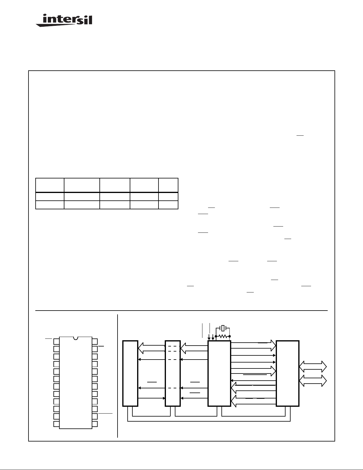
Typical CDP 18 02 Mi croproce ss or Syst em
/SR
ADDR BUS
TPA
MRD
CEO
ADDR BUS
TPA
RAMROM
MRD
MWR
BIDIRECTIONAL DATA BUS
1
WAI
CLEAR
CPU
CDP1802
FIGURE 1.
N0 - N2 MRD
TPB
Q
SC0 SC1
INTERRUPT
DMA - IN DMA - OUT
EF1 - EF4
I/O
CDP1852
File Number
DATA
CONTROL
1166.2

CDP1852, CDP1852C
Absolute Maximum Ratings Thermal Information
DC Supply-voltage Range, (VDD)
(Voltage Referenced to V
Terminal)
SS
CDP1852 . . . . . . . . . . . . . . . . . . . . . . . . . . . . . . . . . .-0.5 to +11V
CDP1852C . . . . . . . . . . . . . . . . . . . . . . . . . . . . . . . . . .-0.5 to +7V
Input Voltage Range, All Inputs . . . . . . . . . . . . . . -0.5 to V
DD
+0.5V
DC Input Current, Any One Input . . . . . . . . . . . . . . . . . . . . . . . .±10mA
Device Dissipation Per Output Transistor. . . . . . . . . . . . . . . 100mW
= Full Package-Temperature Range
For T
A
(All Package Type)
CAUTION: Stresses above t hos e l iste d in “Absolute Max imum Ratings” may cause per ma nen t d am age to th e d evi ce . Thi s is a stre ss o nly rat ing and operatio n
of the device at these or any other conditions above those in dica ted in the operational sections of this specification is not implied.
Thermal Resistance (Typical) θ
(oC/W) θJC (oC/W)
JA
PDIP Package. . . . . . . . . . . . . . . . . . . 65 N/A
SBDIP Package. . . . . . . . . . . . . . . . . . 65 20
Operating-Temperature Range (T
Package Type D, H . . . . . . . . . . . . . . . . . . . . . . . -55
Package Type E . . . . . . . . . . . . . . . . . . . . . . . . . .-40
Storage Temperature Range (T
)
A
) . . . . . . . . . . . . -65oC to +150oC
STG
o
C to +125oC
o
C to +85oC
Lead Temperature (During Soldering): . . . . . . . . . . . . . . . . . +265
At Distance 1/16 ± 1/32 inch (1.59 ± 0.79mm)
from Case for 10s max
o
C
Operating Conditions At T
= Full Package Temperature Range. For Maximum Reliability, Operating Conditions Should be
A
Selected so that Operation is Always within the Following Ranges:
LIMITS
CDP1852 CDP1852C
PARAMETER
MIN MAX MIN MAX
DC Operating Voltage Range 4 10.5 4 6.5 V
Input Voltage Range V
SS
V
DD
V
SS
V
DD
Functional Diagram
MODE 0 MODE 1
P1 CSI CSI
P23 SR SR
CSI/CSI
(NOTE 1)
CS2
MODE
CLOCK
CLEAR
DI0
DI1
DI2
DI3
DI4
DI5
DI6
DI7
13
11
14
16
18
20
22
1
2
3
5
7
9
DEVICE
SELECT
DECODE
RESET
8-BIT
DATA
REGISTER
CONTROL
LOGIC
CLOCK
23
SR
(NOTE 1)
ENABLE
THREE-
STATE
OUTPUT
DRIVERS
/SR
24
12
V
DD
V
SS
4
DO0
6
DO1
8
DO2
10
DO3
15
DO4
17
DO5
19
DO6
21
DO7
UNITS
V
NOTE:
1. Polarity depends on mode.
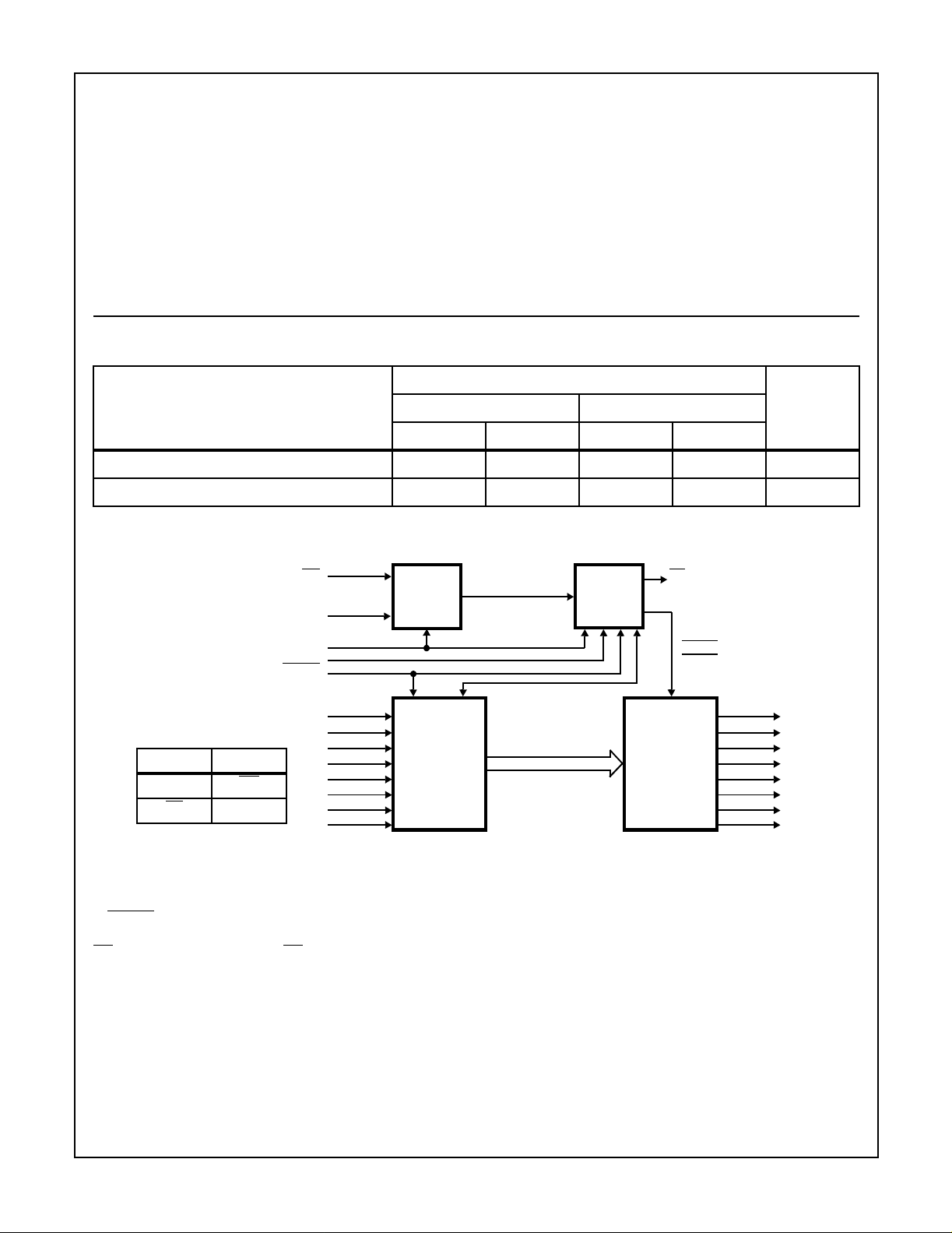
FIGURE 2. FUNCTIONAL BLOCK DIAGRAM FOR CDP1852
A CLEAR control is provided for resetting the port’s register
(DO0-DO7 = 0) and service request flip-flop (input mode:
SR/ SR = 1 and output mode: SR/SR = 0).
The CDP1852 is functionally identical to the CDP1852C.
The CDP1852 has a recommended operating voltage range
of 4 to 10.5 volts, and the CDP1852C has a recommended
operating voltage range of 4 to 6.5 volts.
The CDP1852 and CDP1852C are supplied in 24-lead,
hermetic, dual-in-line ce ramic p ack ages (D suf fix), in 24-lead
dual-in-line plastic packages (E suffix). The CDP1852C is
also available in chip form (H suffix).
2

Logic Diagram
13
CS2
MODE
1
2
14
CS1/CS1
CLEAR
CDP1852, CDP1852C
V
SS
SR/SR
23
S
D
Q
R
CL
SERVICE
REQUEST
LATCH
DI0
DI1
DI7
11
3
5
22
CLOCK
Static Electrical Specifications At T
p
TG
n
p
TG
n
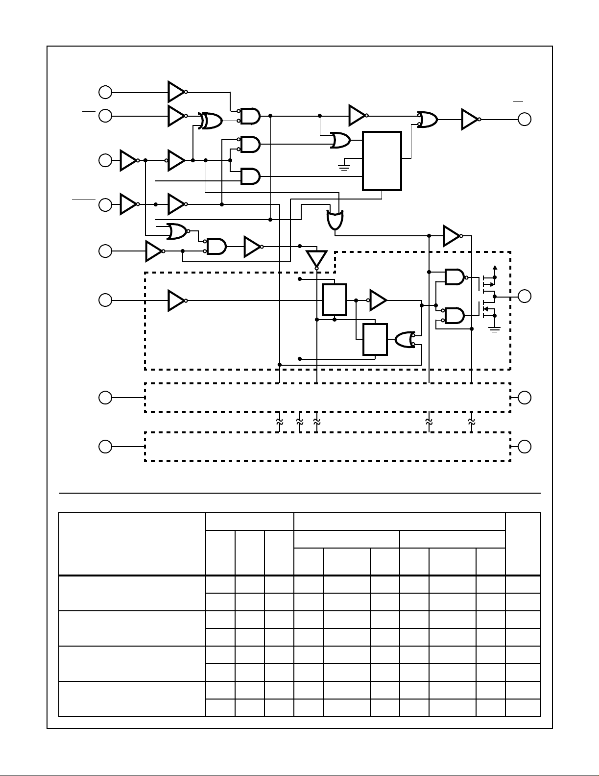
FIGURE 3. CDP1852 LOGIC DIAGRAM
= -40oC to +85oC, Unless Otherwise Specified
A
CONDITIONS LIMITS
V
DD
p
DO0
4
n
V
SS
DO1
6
DO7
21
PARAMETER
Quiescent Device Current I
Output Low Drive
(Sink) Current
Output High Drive
(Source) Current
Output Voltage Low-Level
(Note 2)
CDP1852 CDP1852C
V
DD
(V)
V
IN
DD
(V)
MIN
V
(V)
O
-0, 55--10--50µA
(NOTE1)
TYP MAX MIN
(NOTE1)
TYP MAX
UNITS
- 0, 10 10 - - 100 - - - µA
I
0.4 0, 5 5 1.6 3.2 - 1.6 3.2 - mA
OL
0.5 0, 10 10 3 6 - - - - mA
I
4.6 0, 5 5 -1.15 -2.3 - -1.15 -2.3 - mA
OH
9.5 0, 10 10 -3 -6 - - - - mA
V
OL
- 0, 5 5 - 0 0.1 - 0 0.1 V
- 0, 10 10 - 0 0.1 - - - V
3
 Loading...