Intersil Corporation CDP1852-3 Datasheet

CDP1852/3,
CDP1852C/3
March 1997
Features
• Static Silicon-Gate CMOS Circuitry
• Parallel 8-Bit Data Register and Buffer
• Handshaking Via Service Request Flip-Flop
• Low Quiescent and Operating Power
• Interfaces Directly with CDP1800-Series Microprocessors
• Single Voltage Supply
• Full Military Temperature Range
o
C to +125oC)
(-55
Ordering Information
TEMP.
PACKA GE
SBDIP -55oC to +125oC CDP1852CD3 CDP1852D3 D24.6
RANGE 5V 10V
Pinout
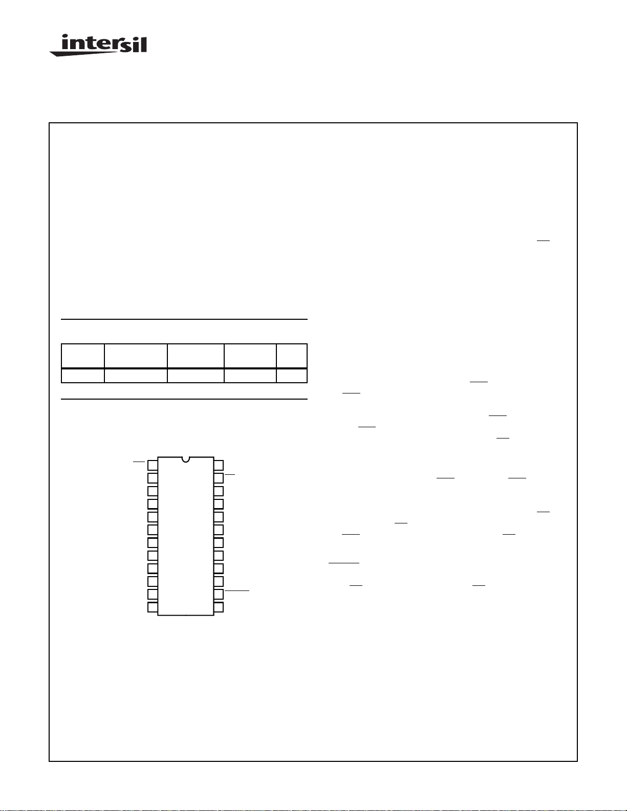
CDP1852/3, CDP1852C/3 (SBDIP)
TOP VIEW
High-Reliability Byte-Wide Input/Output Port
Description
The CDP1852/3 and CDP1852C/3 are parallel, 8-bit, modeprogrammable input/output ports. They are compatible and
will interface directly with CDP1800-Series microprocessors.
They are also useful as 8-bit address latches when used
with the CDP1800 multiplexed address bus and as I/O ports
in general-purpose applications.
The mode control is used to program the device as an input
PKG.
NO
port (mode = 0) or as an output port (mode = 1). The
output can be used as a signal to indicate when data is
ready to be transferred. In the input mode, a peripheral
device can strobe data into the CDP1852/3, and microprocessor can read that data by device selection. In the output
mode, a microprocessor strobes data into the CDP1852/3,
and handshaking is established with a peripheral device
when the CDP1852/3 is deselected.
In the input mode, data at the data-in terminals (DI0-DI7) is
strobed into the port’s 8-bit register by a high (1) level on the
clock line. The negative high-to-low transition of the clock
latches the data in the register and sets the service request
output low (SR/SR = 0). When CS1/
(CS1/
CS1 and CS2 = 1), the three-state output drivers are
CS1 and CS2 are high
enabled and data in the 8-bit register appear at the data-out
terminals (DO0-DO7). When either CS1/
low (CS1/
CS1 or CS2 = 0), the data-out terminals are tristated
and the service request output returns high (
CS1 or CS2 goes
SR/SR =1).
SR/SR
CSI
CSI/
MODE
DI0
DO0
DI1
DO1
DI2
DO2
DI3
DO3
CLOCK
V
1
2
3
4
5
6
7
8
9
10
11
12
SS
24
23
22
21
20
19
18
17
16
15
14
13
V
DD
SR/SR
DI7
DO7
DI6
DO6
DI5
DO5
DI4
DO4
CLEAR
CS2
In the output mode, the output drivers are enabled at all
times. Data at the data-in terminals (DI0-DI7) is strobed into
the 8-bit register when CS1/
CS1 is low (CS1/CS1 = 0) and
CS2 and the clock are high (1), and are present at the dataout terminals (DO0-DO7). The negative high-to-low transition of the clock latches the data in the register. The
output goes high (
(CS1/
CS1 = 1 or CS2 = 0) and retur ns low (SR/SR = 0) on
SR/SR = 1) when the device is deselected
SR/SR
the following trailing edge of the clock.
A
CLEAR control is provided for resetting the port’s register
(DO0-DO7 = 0) and service request flip-flop (input
mode:
SR/SR = 1 and output mode: SR/SR = 0).
The CDP1852/3 is functionally identical to the CDP1852C/3.
The CDP1852/3 has a recommended operating voltage
range of 4V to 10.5V, and the CDP1852C/3 has a recommended operating voltage range of 4V to 6.5V.
The CDP1852/3 and CDP1852C/3 are supplied in 24-lead,
dual-in-line side-brazed ceramic packages (D suffix).
CAUTION: These devices are sensitive to electrostatic discharge; follow proper IC Handling Procedures.
http://www.intersil.com or 407-727-9207
| Copyright © Intersil Corporation 1999
4-28
File Number
1694.2

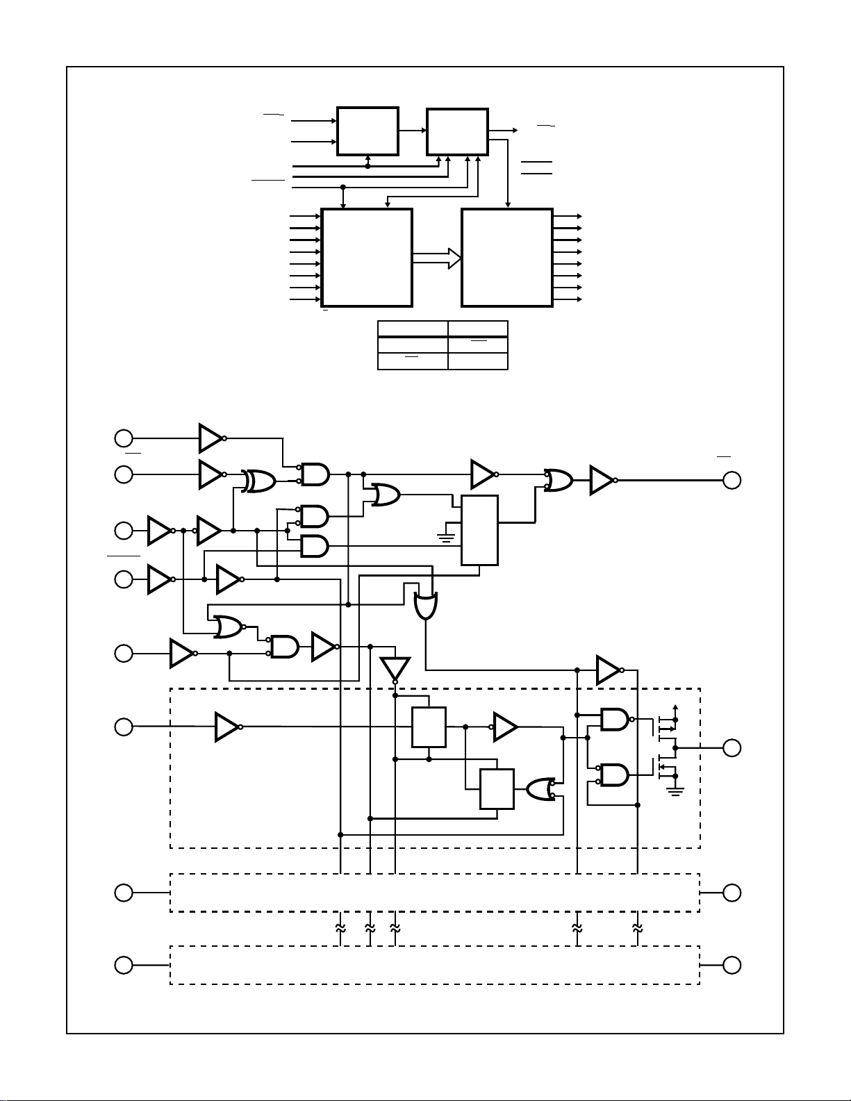
Block Diagram of CDP1852/3
CS2
MODE
CLEAR
1
13
2
11
14
CSI/CSI†
CLOCK
CDP1852/3, CDP1852C/3
DEVICE
SELECT
DECODE
CONTROL
LOGIC
23
SR/
24
12
SR†
V
DD
V
SS
CS2
13
CSI/
CSI
1
MODE
2
CLEAR
14
DI0
DI1
DI2
DI3
DI4
DI5
DI6
DI7
3
RESET CLOCK ENABLE
5
7
9
16
18
20
22
8-BIT
DAT A
REGISTER
† POLARITY DEPENDS ON MODE
MODE = 0
P1
P23
CSI
SR
FIGURE 1.
V
SS
THREE-
OUTPUT
DRIVERS
MODE = 1
CSI
SR
S
Q
D
R
CL
STATE
SERVICE
REQUEST
LATCH
4
DO0
6
DO1
8
DO2
10
DO3
15
DO4
17
DO5
19
DO6
21
DO7
SR/SR
23
CLOCK
11
DI0
3
DI1
5
D17
22
P
TG
N
P
TG
N
FIGURE 2. CDP1852/3 LOGIC DIAGRAM
V
DD
P
DO0
4
N
V
SS
DO1
6
DO7
21
4-29

CDP1852/3, CDP1852C/3
:
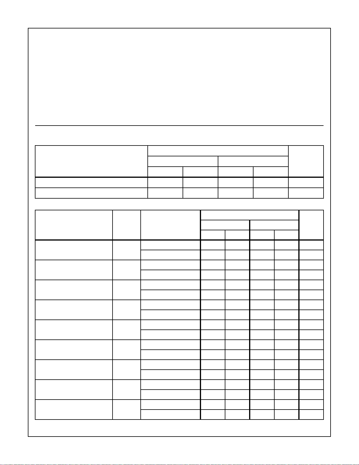
Absolute Maximum Ratings Thermal Information
DC Supply Voltage Range, (VDD):
(All Voltages Referenced to VSS Terminal)
CDP1852/3 . . . . . . . . . . . . . . . . . . . . . . . . . . . . . . . -0.5V to +11V
CDP1852C/3. . . . . . . . . . . . . . . . . . . . . . . . . . . . . . . -0.5V to +7V
Input Voltage Range, All Inputs . . . . . . . . . . . . . -0.5V to VDD +0.5V
DC Input Current, any One Input. . . . . . . . . . . . . . . . . . . . . . . . .±10mA
CAUTION: Stresses above those listed in “Absolute Maximum Ratings” may cause permanent damage to the device. This is a stress only rating and operation
of the device at these or any other conditions above those indicated in the operational sections of this specification is not implied.
Recommended Operating Conditions T
= Full-Package Temperature Range. For maximum reliability, operating conditions
A
should be selected so that operation is always within the following ranges.
Thermal Resistance (Typical) θJA (oC/W) θJC (oC/W)
SBDIP Package. . . . . . . . . . . . . . . . . . 65 20
Device Dissipation Per Output Transistor
TA = Full Package Temperature Range
(All Package Types). . . . . . . . . . . . . . . . . . . . . . . . . . . . . . 100mW
Operating Temperature Range (TA)
Package Type D. . . . . . . . . . . . . . . . . . . . . . . . . .-55oC to +125oC
Storage Temperature Range (T
) . . . . . . . . . . . .-65oC to +150oC
STG
Lead Temperature (During Soldering):
At distance 1/16 ± 1/32 in (1.59 ± 0.79mm)
From Case for 10s max. . . . . . . . . . . . . . . . . . . . . . . . . . . +265oC
LIMITS
CPP1852/3 CDP1852C/3
PARAMETER
MIN MAX MIN MAX
DC Operating Voltage Range 4 10.5 4 6.5 V
Input Voltage Range V
Static Electrical Specifications V
= 0 or VDD, Except as Noted
IN
SS
V
DD
V
SS
V
DD
LIMITS
-55oC, +25oC +125oC
PARAMETER SYMBOL TEST CONDITIONS
Quiescent Device Current (Note 1) I
DD
VDD = 5V - 10 - 100 µA
MIN MAX MIN MAX
VDD = 10V - 20 - 300 µA
Output Low Drive (Sink) Current I
OL
VDD = 5V, VO = 0.4V 2.6 - 1.9 - mA
VDD = 10V, VO = 0.5V 6.1 - 4.1 - mA
Output High Drive (Source) Current I
OH
VDD = 5V, VO = 4.6V -1.8 - -1.3 - mA
VDD = 10V, VO = 9.5V -4.4 - -2.9 - mA
Output Voltage Low Level V
VDD = 5V, IOL = 0µA - 0.1 - 0.2 V
OL
VDD = 10V, IOL = 0µA - 0.1 - 0.2 V
Output Voltage High Level V
VDD = 5V, IOL = 0µA 4.9 - 4.8 - V
OH
VDD = 10V, IOL = 0µA 9.9 - 9.8 - V
Input Low Voltage V
VDD = 5V, VO = 0.2, 4.8V - 1.5 - 1.5 V
IL
VDD = 10V, VO = 0.2, 9.8V - 3 - 3 V
Input High Voltage V
VDD = 5V, VO = 0.2, 4.8V 3.5 - 3.5 - V
IH
VDD = 10V, VO = 0.2, 9.8V 7 - 7 - V
Input Leakage Low I
VDD = 5V, VIN = 0V - -1 - -5 µA
IL
VDD = 10V, VIN = 0V - -1 - -5 µA
Input Leakage High I
VDD = 5V, VIN = 5V - 1 - 5 µA
IH
VDD = 10V, VIN = 10V - 1 - 5 µA
UNITS
V
UNITS
4-30
 Loading...