

March 1997
CDP1826C
CMOS 64-Word x 8-Bit
Static RAM
Features
• Ideal for Small, Low-Power RAM Memory Requirements in Microprocessor and Microcomputer Applications
• Interfaces with CDP1800-Series Microprocessors
Without Additional Address Decoding
• Daisy Chain Feature to Further Reduce External
Decoding Needs
• Multiple Chip-Select Inputs for Versatility
• Single Voltage Supply
• No Clock or Precharge Required.
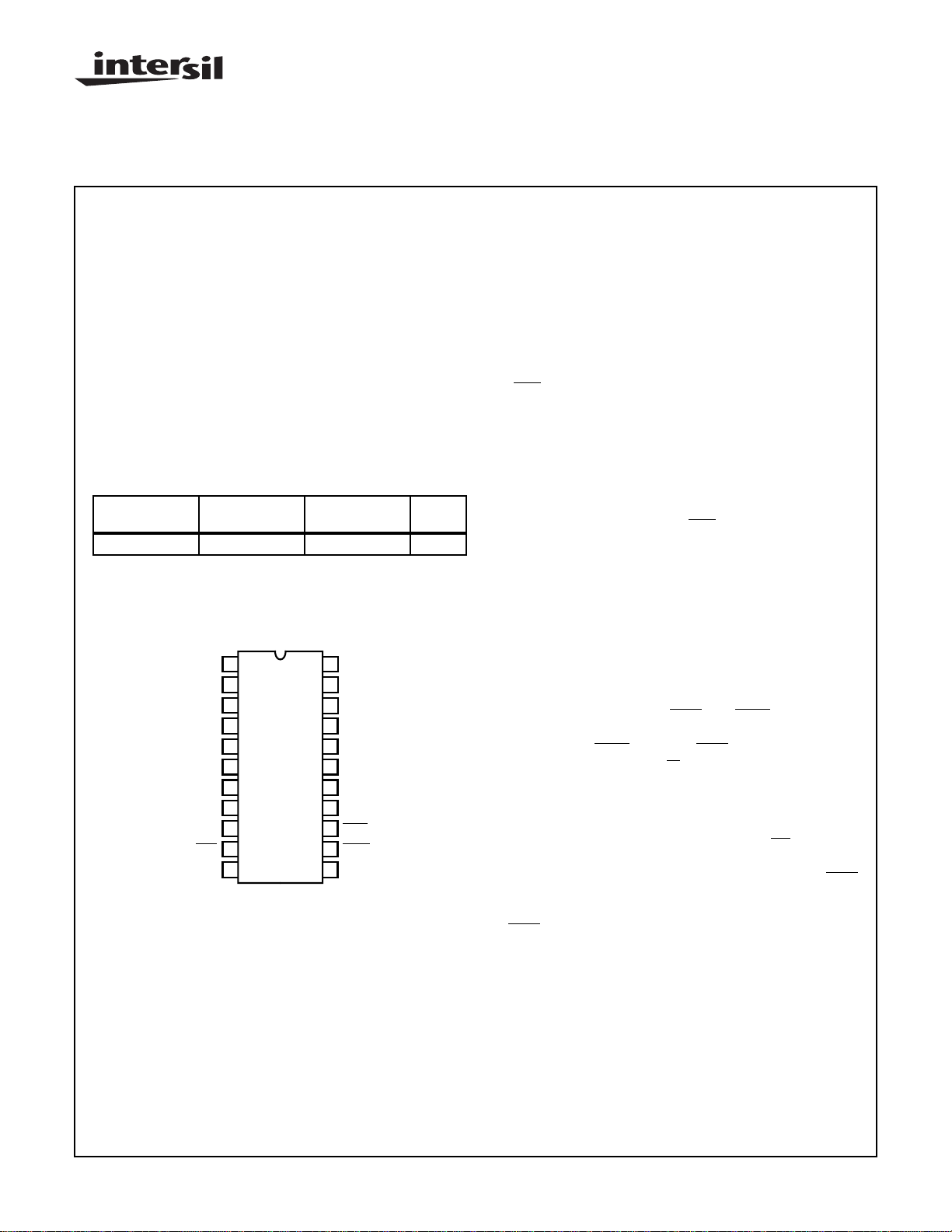
Ordering Information
PKG.
PACKAGE TEMP. RANGE PART NUMBER
PDIP -40oC to +85oC CDP1826CE E22.4
NO.
Pinout
CDP1826C (PDIP)
TOP VIEW
V
BUS 0
BUS 1
BUS 2
BUS 3
BUS 4
BUS 5
BUS 6
BUS 7
CS1
CS2
V
SS
1
2
3
4
5
6
7
8
9
10
11
22
21
20
19
18
17
16
15
14
13
12
DD
A0
CS/A5
A1
A2
A3
A4
TPA
MRD
MWR
CEO
Description
The CDP1826C is a general purpose, fully static, 64-word x
8-bit random-access memory, for use in CDP1800-series or
other microprocessor systems where minimum component
count and/or price performance and simplicity in use are
desirable.
The CDP1826C has 8 common data input and data-output
terminals with three-state capability for direct connection to a
standard bidirectional data bus. Two chip-select inputs - CS1
and
CS2 - are provided to simplify memory-system expansion. An additional select pin, CS/A5, is provided to enable
the CDP1826C to be selected directly from the CDP1800
multiplexed address bus without additional latching or
decoding. In an 1800 system, the CS/A5 pin can be tied to
any MA address line from the CDP1800 processor. A TPA
input is provided to latch the high-order bit of this address
line as a chip-select for the CDP1826C. If this CS/A5 input is
latched high, and if CS = 1 and
time in the memory cycle, the CDP1826C will be enabled for
writing or reading. In a non-1800 system, the TPA pin can be
tied high, and the CS/A5 pin can be used as a normal
address input.
The six input-address buffers are gated with the chip-select
function to reduce standby current when the device is deselected, as well as to provide for a simplified power down
mode by reducing address buffer sensitivity to long fall times
from address drivers which are being powered down.
Two memor y control signals,
for reading from the writing to the CDP1826C. The logic is
designed so that
MWR overrides MRD, allowing the chip to
be controlled from a single R/
A CHIP ENABLE OUTPUT is provided for daisy-chaining to
additional memories or I/O devices. This output is high
whenever the chip-select function selects the CDP1826C,
which deselects any other chip which has its
nected to the CDP1826C CEO output. The connected chip is
selected when the CDP1826C is deselected and the
input is low. Thus, the CEO is only active for a read cycle
and can be setup so that a CEO of another device can feed
the
MRD of the CDP1826C, which in turn selects a third chip
in the daisy chain.
CS2 = 0 at the appropriate
MRD and MWR, are provided
W.
CS input con-
MRD
The CDP1826C has a recommended operating voltage of
4.5V to 5.5V and is supplied in 22 lead dual-in-line plastic
packages (E suffix). The CDP1826C is also available in chip
form (H suffix).
CAUTION: These devices are sensitive to electrostatic discharge; follow proper IC Handling Procedures.
http://www.intersil.com or 407-727-9207
| Copyright © Intersil Corporation 1999
6-47
File Number 1311.2
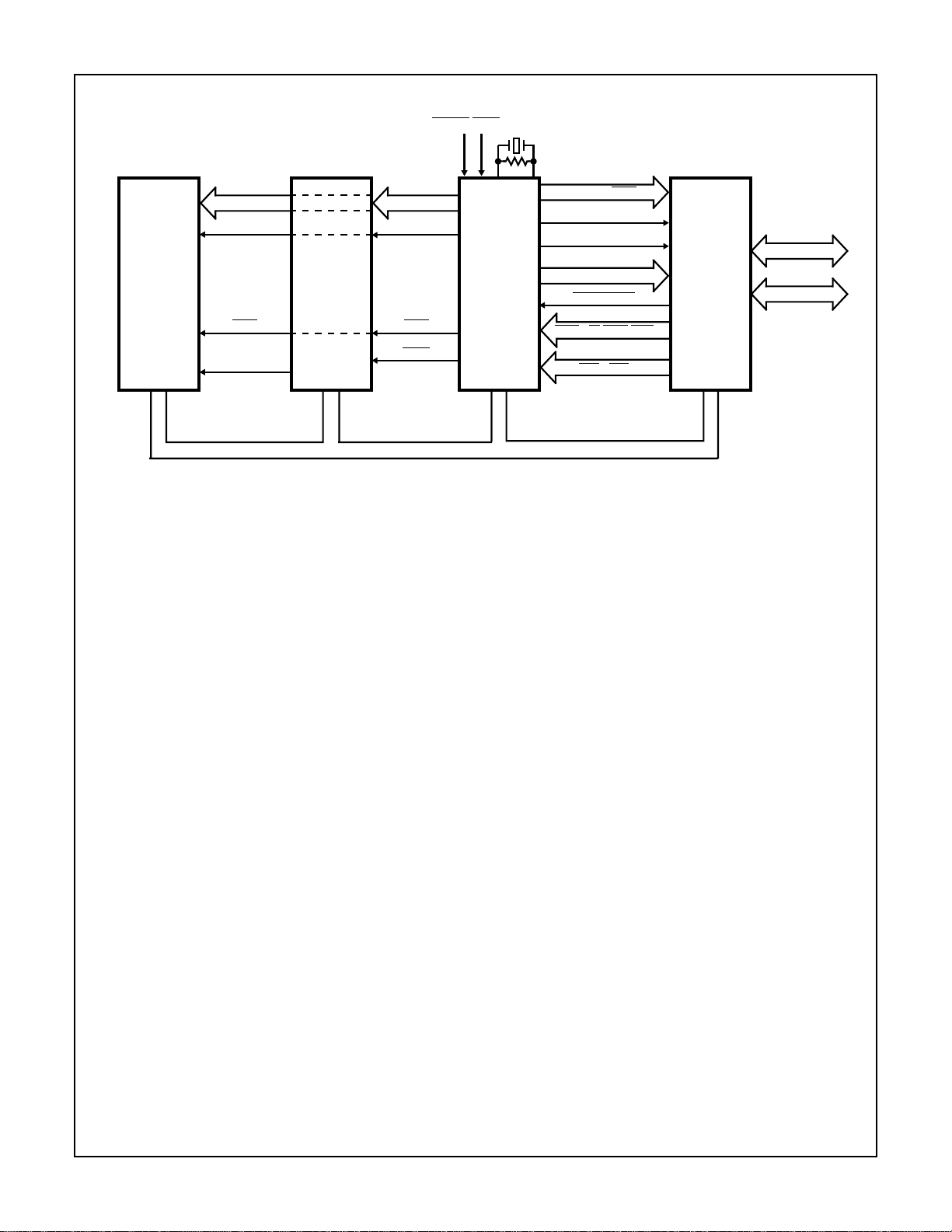
ROM
ADDR BUS
TPA
RAM
CDP1826C
CDP1826C
CLEAR WAIT
ADDR BUS
TPA
CPU
CDP1800
SERIES
MRD
N0 - N2
TPB
Q
SCO SCI
INTERRUPT
I/O
DAT A
CONTROL
MRD
CEO
MRD
MWR
8-BIT BIDIRECTIONAL DATA BUS
DMA - IN DMA OUT
EF1 - EF4
FIGURE 1. TYPICAL CDP1802 MICROPROCESSOR SYSTEM
6-48
CDP1826C
Absolute Maximum Ratings Thermal Information
DC Supply Voltage Range, (VDD)
(All Voltages Referenced to VSS Terminal)
CDP1826C. . . . . . . . . . . . . . . . . . . . . . . . . . . . . . . . -0.5V to +7V
Input Voltage Range, All Inputs . . . . . . . . . . . . .-0.5V to VDD +0.5V
DC Input Current, Any One Input. . . . . . . . . . . . . . . . . . . . . . . . .±10mA
Power Dissipation Per Package (PD)
TA = -40oC to +60oC (Package Type E) . . . . . . . . . . . . . . 500mW
TA = +60oC to +85oC (Package Type E). . . . . . Derate Linearly at
12mW/oC to 200mW
TA = -55oC to +100oC (Package Type D) . . . . . . . . . . . . . 500mW
TA = +100oC to +125oC (Package Type D). . . . Derate Linearly at
12mW/oC to 200mW
Thermal Resistance (Typical) θJA (oC/W) θJC (oC/W)
PDIP Package. . . . . . . . . . . . . . . . . . . 75 N/A
Device Dissipation Per Output Transistor
TA = Full Package Temperature Range
(All Package Types). . . . . . . . . . . . . . . . . . . . . . . . . . . . . .100mW
Operating Temperature Range (TA)
Package Type D. . . . . . . . . . . . . . . . . . . . . . . . . .-55oC to +125oC
Package Type E. . . . . . . . . . . . . . . . . . . . . . . . . . .-40oC to +85oC
Storage Temperature Range (T
Lead Temperature (During Soldering)
At distance 1/16 ±1/32 In. (1.59 ±0.79mm)
from case for 10s max. . . . . . . . . . . . . . . . . . . . . . . . . . . . +265oC
). . . . . . . . . . . .-65oC to +150oC
STG
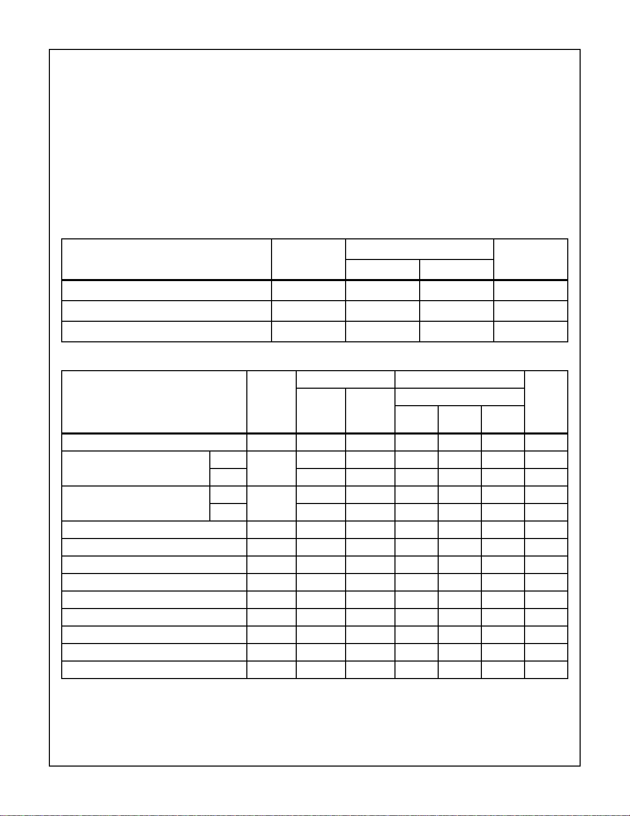
Recommended Operating Conditions At T
= Full Package Temperature Range. For maximum reliability, operating conditions
A
should be selected so that operation is always within the following ranges:
CDP1826C
PARAMETER SYMBOL
UNITSMIN MAX
DC Operating Voltage Range 4 6.5 V
Input Voltage Range V
Input Signal Rise or Fall Time, VDD = 5V tR, t
Static Electrical Specifications At T
= -40oC to +85oC, VDD = 5V ±5%, Except as Noted:
A
F
SS
-10µs
V
DD
CONDITIONS LIMITS
CDP1826C
PARAMETER SYMBOL
Quiescent Device Current I
Output Low (Sink) Current BUS I
CEO 0.4 0, V
Output High (Source) Current BUS I
CEO VDD -0.4 0, V
Output Voltage Low-Level V
Output Voltage High-Level V
Input Low Voltage V
Input High Voltage V
Input Leakage Current I
Operating Device Current (Note 2) I
OPER
Three-State Output Leakage Current I
Input Capacitance C
Output Capacitance C
DD
OL
OH
OL
OH
IL
IH
IN
OUT
IN
OUT
V
O
(V)
- 0, V
0.4 0, V
VDD -0.4 0, V
- 0, V
- 0, V
- - - - 1.5 V
- - 3.5 - - V
Any Input 0, V
- 0, V
0, V
DD
- - - 5 7.5 pF
- 0, V
V
0, V
(V)
IN
MIN
DD
DD
DD
DD
DD
DD
DD
DD
DD
DD
DD
1.6 3.2 - mA
0.8 1.6 - mA
-1.0 -1.5 - mA
-0.6 -1.0 - mA
VDD -0.1 V
(NOTE 1)
TYP MAX
-550µA
- 0 0.1 V
DD
-V
- ±0.1 ±1 µA
- 5 10 mA
- ±0.1 ±1 µA
-1015pF
NOTES:
1. Typical values are for TA = +25oC and nominal VDD.
2. Outputs open circuited; Cycle time = 1µs.
V
UNITS
6-49

Signal Descriptions
CDP1826C
A0 - A4, CS/A5 (Address Inputs): These inputs must be
stable prior to a write operation, but may change asynchronously during Read operations.
In an 1800 system, the multiplexed high-order address bit at
pin CS/A5 can be latched at the end of TPA. A high level will
provide a valid chip select for the CDP1826C. The low-order
address bit which appears after TPA is used for data word
selection. In non-1800 systems, TPA can be tied high to disable the latch and allow the CS/A5 pin to function as a normal address input.
BUS 0 - BUS 7: 8-bit three-state common input/output data
bus.
TPA: High-order address strobe input. The high-order
address bit at input CS/A5 is latched on the high-to-low tran-
A0
A1
A2
A3
A4
CS/A5
INPUT
ADDRESS
BUFFERS
XY
DECODE
sition of the TPA input. Tie TPA high to disable the CS/A5
latch feature.
CS1,
CS2 (Chip Selector): Either chip select (CS1 or CS2),
when not valid, powers down the chip, disables READ and
WRITE functions, and gates off the address and output buffers .
MRD, MWR: Read and Write control signals. MWR overrides
MRD, allowing the CDP1826C to be controlled from a
single R/
W line.
CEO (Chip Enable Output): Allows daisy chaining to additional memories. CEO is high whenever the CDP1826C is
selected. CEO is only active (low) for a Read cycle with the
CDP1826C deselected and the
, VSS: Power supply connections.
V
DD
INPUT/OUTPUT
64 x 8
MATRIX
BUFFERS
CONTROL
DAT A
AND
MRD input low.
BUS 0
BUS 1
BUS 2
BUS 3
BUS 4
BUS 5
BUS 6
BUS 7
TPA
CS1
CS2
MWR
MRD
D
Q
C
CEO
FIGURE 2. FUNCTIONAL DIAGRAM
6-50

1800 CLOCK
A5
TPA
MRD
CEO
CDP1826C
BUS
CS1 = 1,
RAM CYCLE
CS2 = 0
VALID DATA
(RAM SELECTED) ROM CYCLE (RAM DESELECTED)
VALID DATA
OPERATING MODES
(NOTE 1)
FUNCTION MRD MWR CS1 • CS2 TPA
CS/A5 CEO
CDP1800 Mode Write X O I I I
Read O I I I I
Deselect I I I I I
Deselect I X O X X I
Deselect O X O X X O
Deselect I X X O I
Deselect O X X O O
Non-CDP1800 Mode Write X O I I X I
Read O I I I X I
Deselect I I I I X I
Deselect I X O I X I
Deselect O X O I X O
NOTE:
1. For CDP1800 Mode, ref ers to high order memory address bit level at time when TPA transition takes
place.
FIGURE 3. CHIP ENABLE OUTPUT TIMING WAVEFORMS FOR CDP1800 BASED SYSTEMS
6-51

CDP1826C
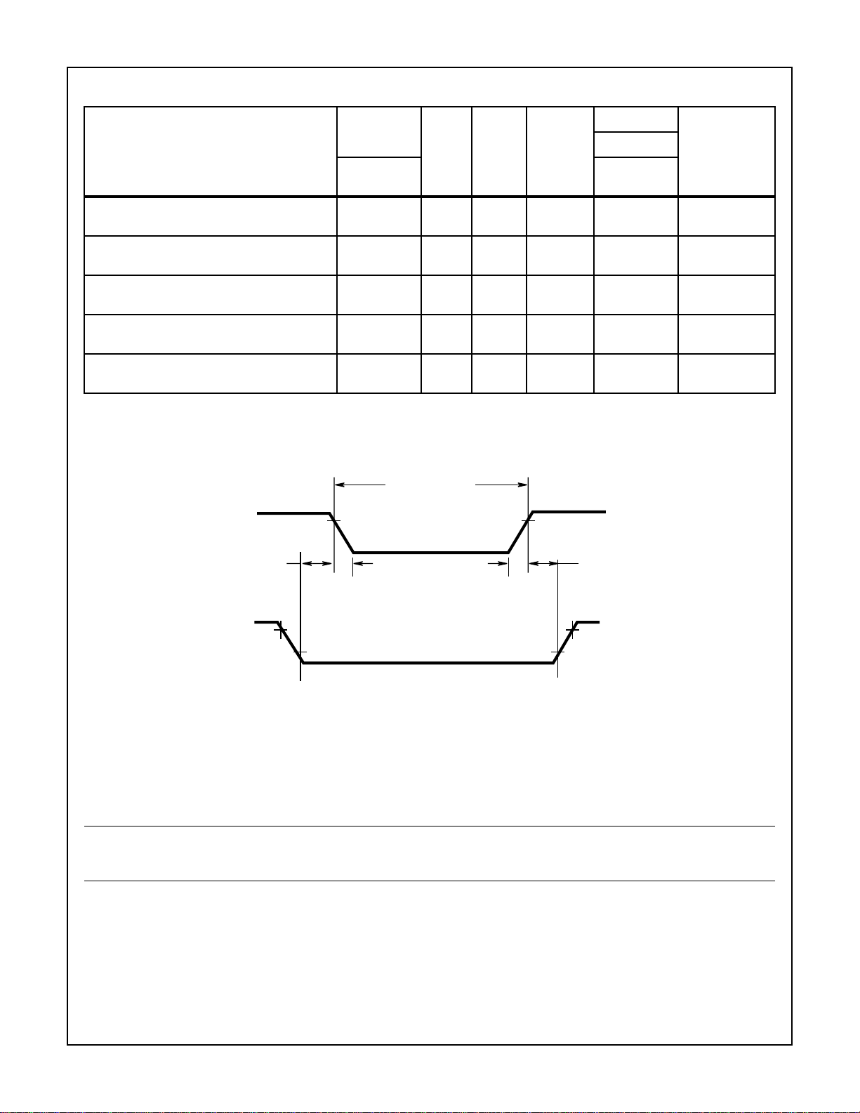
Dynamic Electrical Specifications At T
= -40 to +85oC, VDD = 5V ±5%, Input tR, tF = 10ns; CL = 50pF and 1 TTL Load
A
PARAMETER
READ - CYCLE TIMES (FIGURES 4 AND 5)
Address to TPA Setup t
Address to TPA Hold t
Access from Address Change T
TPA Pulse Width t
Output Valid from MRD t
Access from Chip Select t
CEO Delay from TPA Edge t
MRD to CEO Delay t
Output High Z from Invalid MRD t
Output High Z from Chip Deselect t
ASH
AH
AA
PAW
AM
AC
CA
MC
RHZ
SHZ
NOTES:
1. Time required by a limit device to allow tor the indicated function.
2. Typical values are or TA = 25oC and nominal VDD.
LIMITS
CDP1826C
(NOTE 1)
MIN
(NOTE 2)
TYP MAX
100 - - ns
100 - - ns
- 500 1000 ns
200 - - ns
- 500 1000 ns
- 500 1000 ns
- 150 300 ns
75 - - ns
- - 125 ns
- - 225 ns
UNITS
A0 - A5 LOW ORDER ADDRESS BYTE
TPA
MRD
CS2
CS1 -
CEO
BUS
HIGH ORDER
ADDRESS BYTE
t
ASH
t
PAW
t
AH
t
CA
t
MC
HIGH IMPEDANCE
t
AM
t
AA
t
AC
VALID CHIP SELECT
FIGURE 4. TIMING WAVEFORMS FOR READ CYCLE 1
VALID DATA
t
RHZ
t
SHZ
6-52

CDP1826C
A0 - A5
CS1 •
MRD
CS2
BUS
HIGH ORDER
ADDRESS BYTE
FIGURE 5. TIMING WAVEFORMS FOR READ-CYCLE 2 (TPA HIGH)
Dynamic Electrical Specifications At T
LOW ORDER ADDRESS BYTE
t
AA
t
AC
VALID CHIP SELECT
HIGH IMPEDANCE
t
AM
= -40 to +85oC, VDD = 5V ± 5%,Input tR, tF = 10ns; CL = 50pF and 1 TTL Load
A
VALID DATA
t
RHZ
t
SHZ
LIMITS
PARAMETER
WRITE - CYCLE TIMES (FIGURES 6 AND 7)
Address to TPA Setup, High Byte t
Address to TPA Hold t
Address Setup, Low Byte T
TPA Pulse Width t
Chip Select Setup t
Write Pulse Width t
Write Recovery t
Data Setup t
Data Hold from End of MWR t
Data Hold from End of Chip Select t
ASH
AH
ASL
PAW
CS
WW
WR
DS
DH1
DH2
NOTES:
1. Time required by a limit device to allow tor the indicated function.
2. Typical values are for TA = 25oC and nominal VDD.
CDP1826C
(NOTE 1)
MIN
(NOTE 2)
TYP MAX
100 - - ns
100 - - ns
500 250 - ns
200 - - ns
700 350 - ns
300 200 - ns
100 - - ns
400 200 - ns
100 50 - ns
125 50 - ns
UNITS
6-53

CDP1826C
A0 - A5
CS1 •
TPA
MWR
CS2
BUS
HIGH ORDER
ADDRESS BYTE
t
ASH
t
PAW
t
AH
LOW ORDER ADDRESS BYTE
t
ASL
t
CS
VALID CHIP SELECT
t
DS
DATA IN STABLE
FIGURE 6. TIMING WAVEFORMS FOR WRITE-CYCLE 1
t
WW
t
WR
t
DH1,tDH2
A0 - A5
CS1 •
MWR
CS2
BUS
HIGH ORDER
ADDRESS BYTE
LOW ORDER ADDRESS BYTE
t
ASL
t
WW
t
CS
t
WR
VALID CHIP SELECT
t
DS
DATA IN STABLE
FIGURE 7. TIMING WAVEFORMS FOR WRITE-CYCLE 2 (TPA = HIGH)
t
DH1,tDH2
6-54
CDP1826C
Data Retention Specifications At T
= -40 to +85oC, see Figure 8
A
PARAMETER
Minimum Data Retention
Voltage V
DR
Data Retention Quiescent
Current t
DD
Chip Deselect to Data
Retention Time t
CDR
Recovery to Normal
Operation Time t
RC
VDD to VDR Rise and
Fall Time tR,t
F
NOTE:
1. Typical values are or TA = 25oC and nominal VDD.
V
DD
t
CDR
TEST
LIMITS
CONDITIONS
V
DR
(V) MAX
V
DD
(V) MIN
(NOTE 1)
TYP
CDP1826C
- - - 2 2.5 V
2.5 - - 5 25 µA
- 5 600 - - ns
- 5 600 - - ns
2.5 5 1 - - µA
DATA RETENTION
MODE
0.95 V
DD
V
DR
t
F
0.95 V
t
R
DD
t
RC
UNITS
CS1
V
IH
V
IL
V
IH
V
IL
FIGURE 8. LOW VDD DATA RETENTION TIMING WAVEFORMS
All Intersil semiconductor products are manufactured, assembled and tested under ISO9000 quality systems certification.
Intersil products are sold by description only. Intersil Corporation reserves the right to make changes in circuit design and/or specifications at any time without
notice. Accordingly, the reader is cautioned to verify that data sheets are current before placing orders. Information furnished by Intersil is believed to be accurate
and reliable. However, no responsibility is assumed by Intersil or its subsidiaries for its use; nor for any infringements of patents or other rights of third parties which
may result from its use. No license is granted by implication or otherwise under an y patent or patent rights of Intersil or its subsidiaries.
For information regarding Intersil Corporation and its products, see web site http://www.intersil.com
Sales Office Headquarters
NORTH AMERICA
Intersil Corporation
P. O. Box 883, Mail Stop 53-204
Melbourne, FL 32902
TEL: (407) 724-7000
FAX: (407) 724-7240
EUROPE
Intersil SA
Mercure Center
100, Rue de la Fusee
1130 Brussels, Belgium
TEL: (32) 2.724.2111
FAX: (32) 2.724.22.05
ASIA
Intersil (Taiwan) Ltd.
Taiwan Limited
7F-6, No. 101 Fu Hsing North Road
Taipei, Taiwan
Republic of China
TEL: (886) 2 2716 9310
FAX: (886) 2 2715 3029
6-55
 Loading...