March 1997
CDP1824/3,
CDP1824C/3
High-Reliability CMOS 32-Word x 8-Bit
Static Random-Access Memory
Features
• Access Time
- 610ns. . . . . . . . . . . . . . . . . . . . . . . . . . . . . at V
- 320ns. . . . . . . . . . . . . . . . . . . . . . . . . . . . at V
• No Precharge or Clock Required
Ordering Information
PACK-
5V 10V
CDP1824CD3 CDP1824D3 SBDIP -55oC to
Pinout
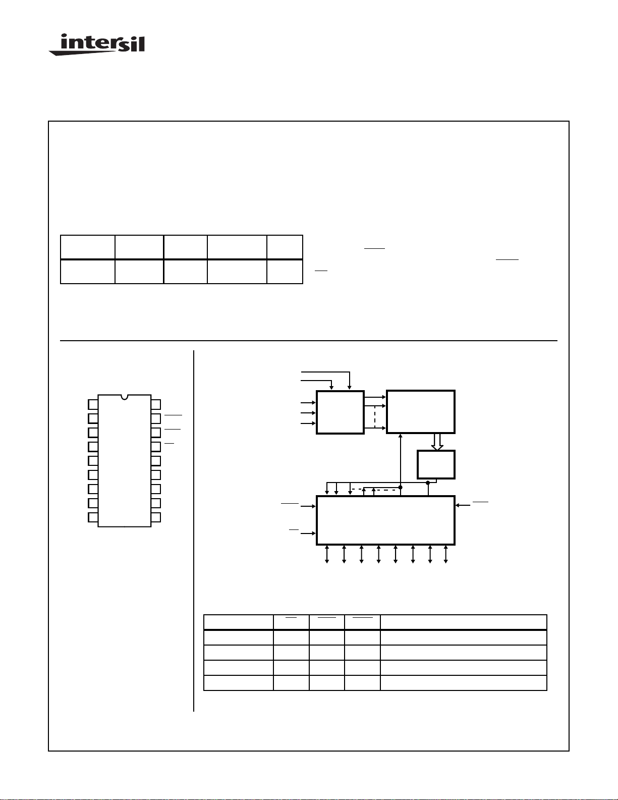
CDP1824/3, CDP1824C/3 (SBDIP)
TOP VIEW
1
MA4
2
MA3
3
MA2
4
MA1
5
MA0
6
BUS7
7
BUS6
8
BUS5
9
V
SS
AGE TEMP. RANGE
Functional Diagram
18
V
DD
17
MWR
16
MRD
15
CS
14
BUS0
13
BUS1
12
BUS2
BUS3
11
10
BUS4
+125oC
DD
DD
D18.3
V
V
= 5V
= 10V
PKG.
NO.
MA4
MA3
MA2
MA1
MA0
MWR
= 18
DD
= 9
SS
Description
The CDP1824/3 and CDP1824C/3 types are high-reliability
CMOS 32-word x 8-bit fully static random-access memories
for use in CDP1800-series microprocessor systems. These
parts are compatible with the CDP1802 microprocessor and
will interface directly without additional components.
The CDP1824/3 is fully decoded and does not require a precharge or clocking signal for proper operation. It has common input and output and is operated from a single voltage
supply. The
three-state output drivers, and overrides the
CS input is provided for memory expansion.
The CDP1824C/3 is functionally identical to the CDP1824/3.
The CDP1824/3 has a recommended operating voltage
range of 4V to 10.5V, and the CDP1824C/3 has an operating
voltage range of 4V to 6.5V.
21
3
ADDRESS
4
DECODER
5
17
I/O BUFFERS
15
CS
6 7 8 10 11 12 13 14
BUS7BUS6BUS5BUS4BUS3BUS2BUS1BUS
MRD signal (output disable control) enables the
MWR signal. A
32 X 8-BIT
ARRAY
SENSE
AMPL
16
MRD
0
OPERATIONAL MODES
FUNCTION CS MRD MWR DATA PINS STATUS
READ 0 0 X Output: High/Low Dependent on Data
WRITE 0 1 0 Input: Output Disabled
Not Selected 1 X X Output Disabled: High-Impedance State
Standby 0 1 1 Output Disabled: High-Impedance State
Logic 1 = High Logic 0 = Low X = Don’t Care
CAUTION: These devices are sensitive to electrostatic discharge; follow proper IC Handling Procedures.
http://www.intersil.com or 407-727-9207
| Copyright © Intersil Corporation 1999
6-42
File Number 1717.2

CDP1824/3, CDP1824C/3
Absolute Maximum Ratings Thermal Information
DC Supply Voltage Range, (VDD)
(All Voltages Referenced to VSS Terminal)
CDP1824/3 . . . . . . . . . . . . . . . . . . . . . . . . . . . . . . . -0.5V to +11V
CDP1824C/3. . . . . . . . . . . . . . . . . . . . . . . . . . . . . . . . .-0.5 to +7V
Input Voltage Range, All Inputs . . . . . . . . . . . . . -0.5V to VDD +0.5V
DC Input Current, Any One Input. . . . . . . . . . . . . . . . . . . . . . . . .±10mA
Thermal Resistance (Typical, Note 1) θJA (oC/W) θJC (oC/W)
SBDIP Package. . . . . . . . . . . . . . . . . . 75 20
Device Dissipation Per Output Transistor
TA = Full Package Temperature Range
(All Package Types). . . . . . . . . . . . . . . . . . . . . . . . . . . . . . 100mW
Operating Temperature Range (TA)
Package Type D. . . . . . . . . . . . . . . . . . . . . . . . . .-55oC to +125oC
Storage Temperature Range (T
Lead Temperature (During Soldering)
At distance 1/16 ±1/32 In. (1.59 ± 0.79mm)
from case for 10s max. . . . . . . . . . . . . . . . . . . . . . . . . . . . +265oC
). . . . . . . . . . . .-65oC to +150oC
STG
Recommended Operating Conditions T
= Full Package-Temperature Range. For maximum reliability, nominal operating con-
A
ditions should be selected so that operation is always within the following ranges:
LIMITS
CDP1824/3 CDP1824C/3
PARAMETER
MIN MAX MIN MAX
UNITS
DC Operating Voltage Range 4 10.5 4 6.5 V
Input Voltage Range V
SS
V
DD
V
SS
V
DD
V
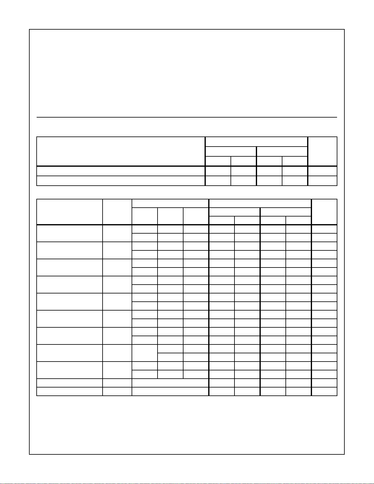
Static Electrical Specifications
CONDITIONS LIMITS
-55oC, +25oC +125oC
MIN MAX MIN MAX
UNITS
PARAMETER SYMBOL
Quiescent Device Current
(Note 1)
Output Voltage Low-Level
(Note 2)
Output Voltage High-Level
(Note 2)
Input Low Voltage V
V
O
(V)
I
DD
- 0, 5 5 - 50 - 500 µA
- 0, 10 10 - 500 - 1000 µA
V
OL
- 0, 5 5 - 0.1 - 0.2 V
- 10 - 0.1 - 0.2 V
V
OH
- 0, 5 5 4.9 - 4.8 - V
- - 10 9.9 - 4.8 - V
IL
0.5, 4.5 - 5 - 1.5 - 1.5 V
V
(V)
IN
V
DD
(V)
1, 9 - 10 - 3 - - V
Input High Voltage V
IH
0.5, 4.5 - 5 3.5 - 3.5 - V
1, 9 - 10 7 - 7 - V
Output Low Drive (Sink)
Current
Output High Drive (Source)
Current
Input Current I
Three-State Output
Leakage Current
Input Capacitance C
Output Capacitance C
I
OL
I
OH
I
OUT
OUT
0.4 0, 5 5 4 - 1.5 - mA
0.5 0, 10 10 4 - 2.9 - mA
4.6 0, 5 5 - -1 - -0.75 mA
9.5 0, 10 10 - -2 - -1.5 mA
IN
Any
Input
0, 55-1-5µA
0, 10 10 - 1 - 5 µA
0, 5 0, 5 5 - 2 - 5 µA
0, 10 0, 10 10 - 2 - 5 µA
IN
(Note 2) - 10 - 10 pF
(Note 2) - 15 - 15 pF
NOTES:
1. The CDP1824C/3 meets all 5V Static Electrical Characteristics of the CDP1824/3 except Quiescent Device Current for which the limits
are IDD = 200µA at +25oC/-55oC; IDD = 1000µA at +125oC.
2. Guaranteed, but not tested.
6-43
 Loading...