Intersil Corporation CDP1824C, CDP1824 Datasheet

CDP1824,
CDP1824C
March 1997
Features
• Fast Access Time
= 5V . . . . . . . . . . . . . . . . . . . . . . . . . . . . . . . 710ns
-V
DD
-V
= 10V . . . . . . . . . . . . . . . . . . . . . . . . . . . . . . 320ns
DD
• No Precharge or Clock Required
Description
The CDP1824 and CDP1824C are 32-word x 8-bit fully static
CMOS random-access memories for use in CDP-1800
series microprocessor systems. These parts are compatible
with the CDP1802 microprocessor and will interface directly
without additional components.
32-Word x 8-Bit Static RAM
The CDP1824 is fully decoded and does not require a precharge or clocking signal for proper operation. It has
common input and output and is operated from a single
voltage supply. The
MRD signal (output disable control)
enables the three-state output drivers, and overrides the
MWR signal. A CS input is provided for memory expansion.
The CDP1824C is functionally identical to the CDP1824.
The CDP1824 has an operating range of 4V to 10.5V, and
the CDP1824C has an operating voltage range of 4V to
6.5V. The CDP1824 and CDP1824C are supplied in 18 lead
hermetic dual-in-line ceramic packages (D suffix), and in 18
lead dual-in-line plastic packages (E suffix).
Ordering Information
5V 10V PACKAGE TEMPERATURE RANGE PKG. NO.
CDP1824CE CDP1824E PDIP -40oC to +85oC E18.3
CDP1824CEX CDP1824EX Burn-In E18.3
CDP1824CD CDP1824D SBDIP -40oC to +85oC D18.3
Pinout
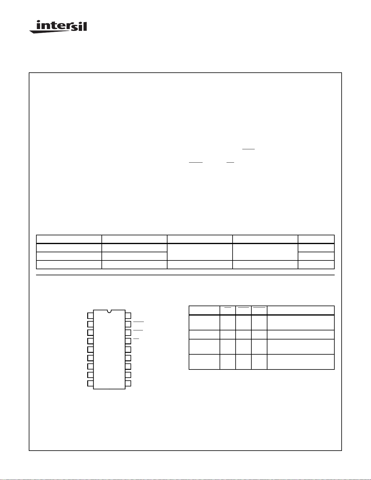
CDP1824, CDP1824C (PDIP, SBDIP)
TOP VIEW
1
MA4
MA3
2
MA2
3
MA1
4
MA0
5
BUS 7
6
BUS 6
7
BUS 5
8
V
9
SS
CAUTION: These devices are sensitive to electrostatic discharge; follow proper IC Handling Procedures.
http://www.intersil.com or 407-727-9207
| Copyright © Intersil Corporation 1999
18
V
DD
17
MWR
16
MRD
15
CS
14
BUS 0
13
BUS 1
12
BUS 2
BUS 3
11
10
BUS 4
FUNCTION CS MRD MWR DATA PINS STATUS
READ 0 0 X Output: High/Low Dependent
WRITE 0 1 0 Input: Output Disabled
Not
Selected
Standby 0 1 1 Output Disabled:
Logic 1 = High Logic 0 = Low X = Don’t Care
6-37
OPERATIONAL MODES
on Data
1 X X Output Disabled:
High-Impedance State
High-Impedance State
File Number 1103.2

CDP1824, CDP1824C
Absolute Maximum Ratings Thermal Information
DC Supply Voltage Range, (VDD)
(All Voltages Referenced to VSS Terminal)
CDP1824 . . . . . . . . . . . . . . . . . . . . . . . . . . . . . . . . -0.5V to +11V
CDP1824C. . . . . . . . . . . . . . . . . . . . . . . . . . . . . . . . -0.5V to +7V
Input Voltage Range, All Inputs . . . . . . . . . . . . .-0.5V to VDD +0.5V
DC Input Current, Any One Input. . . . . . . . . . . . . . . . . . . . . . . . .±10mA
Operating Temperature Range (TA)
Package Type D . . . . . . . . . . . . . . . . . . . . . . . . .-55oC to +125oC
Package Type E . . . . . . . . . . . . . . . . . . . . . . . . . .-40oC to +85oC
Thermal Resistance (Typical) θJA (oC/W) θJC (oC/W)
SBDIP Package. . . . . . . . . . . . . . . . . . 75 20
PDIP Package. . . . . . . . . . . . . . . . . . . 75 N/A
Storage Temperature Range (T
Lead Temperature (During Soldering)
At distance 1/16 ±1/32 In. (1.59 ± 0.79mm)
from case for 10s max. . . . . . . . . . . . . . . . . . . . . . . . . . . .+265oC
). . . . . . . . . . . .-65oC to +150oC
STG
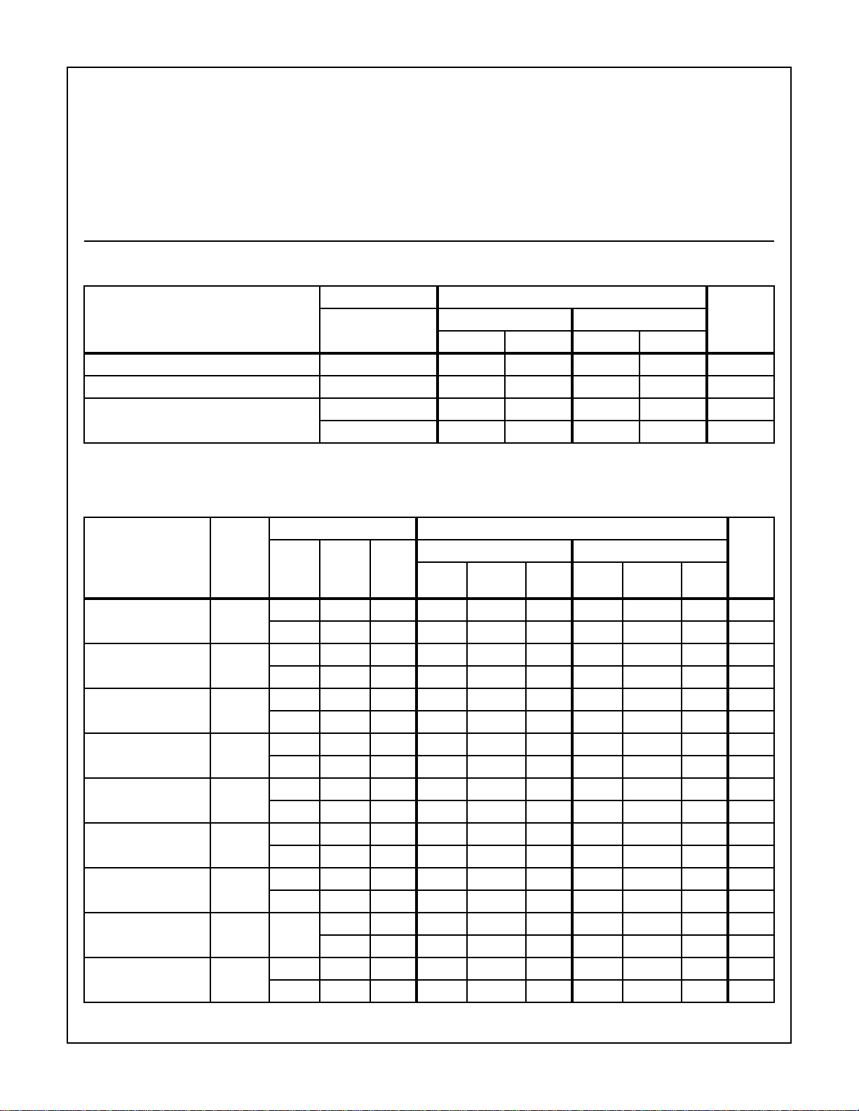
Recommended Operating Conditions At T
= Full Package Temperature Range.F or maxim um reliability, operating conditions
A
should be selected so that operation is always within the following ranges:
CONDITION LIMITS
CDP1824D CDP1824CD
PARAMETER
MIN MAX MIN MAX
UNITSVDD (V)
Supply Voltage Range - 4 10.5 4 6.5 V
Recommended Input Voltage Range - V
SS
V
DD
V
SS
V
DD
Input Signal Rise or Fall Time (Note 1) 5 - 5 - 5 µs
tR, t
F
10 - 2 - - µs
NOTE:
1. Input signal rise or fall times longer than these maxima can cause loss of stored data in either the selected or deselected mode.
Static Electrical Specifications At T
= -40oC to +85oC, Except as Noted:
A
CONDITIONS LIMITS
CDP1824 CDP1824C
PARAMETER SYMBOL
Quiescent Device
Current
Output Low (Sink)
Current
Output High (Source)
Current
Output Voltage
Low-Level
Output Voltage
High-Level
Input Low Voltage V
V
O
(V)
I
DD
- - 5 - 25 50 - 100 200 µA
- - 10 - 250 500 - - - µA
I
OL
0.4 0, 5 5 1.8 2.2 - 1.8 2.2 - mA
0.5 0, 10 10 3.6 4.5 - - - - mA
I
OH
4.6 0, 5 5 -0.9 -1.1 - -0.9 -1.1 - mA
9.5 0, 10 10 -1.8 -2.2 - - - - mA
V
OL
- 0, 5 5 - 0 0.1 - 0 0.1 V
- 0, 10 10 - 0 0.1 - - - V
V
OH
- 0, 5 5 4.9 5 - 4.9 5 - V
- 0, 10 10 9.9 10 - - - - V
0.5, 4.5 - 5 - - 1.5 - - 1.5 V
IL
V
(V)
V
IN
DD
(V)
MIN
(NOTE 1)
TYP MAX MIN
(NOTE 1)
TYP MAX
1.9 - 10 - - 3 - - - V
Input High Voltage V
0.5, 9.5 - 5 3.5 - - 3.5 - - V
IH
1.9 - 10 7 - - - - - V
Input Leakage Current I
Operating Current
(Note 2)
I
DD1
IN
Any
Input
0, 5 5 - ± 0.1 ±1-± 0.1 ± 1 µA
0, 10 10 - ± 0.1 ± 1- - -µA
- 0, 5 5 - 4 8 - 4 8 mA
- 0, 10 10 - 8 16 - - - mA
V
UNITS
6-38
 Loading...