March 1997
CDP1823C/3
High-Reliability CMOS
128-Word x 8-Bit Static RAM
Features
• For Applications in Aerospace, Military, and Critical
Industrial Equipment
• Compatible with CDP1800-Series Microprocessors at
Maximum Speed
• Interfaces with CDP1800-Series Microprocessors
without Additional Components
• Fast Access Time
• At V
= 5V, +25oC . . . . . . . . . . . . . . . . . . . . . . . .275ns
DD
• Single Voltage Supply
• Common Data Inputs and Outputs
• Multiple Chip Select Inputs to Simplify Memory
System Expansion
• High Noise Immunity. . . . . . . . . . . . . . . . . . 30% of V
• Memory Retention for Standby Battery Voltage Down
to 2V at 25
o
C
DD
• Latch-Up-Free Transient Radiation Tolerance
Ordering Information
PART NUMBER
PACKAGE TEMP. RANGE
SBDIP -55oC to +125oC CDP1823CD3 D24.6
(5V) PKG. NO.
Description
The CDP1823C/3 is a 128 word x 8-bit CMOS/SOS static
random access memory. It is compatible with the CDP1802,
CDP1804, CDP1805, and CDP1806 microprocessors, and
will interface directly without additional components. The
CDP1823C has a recommended operating voltage range of
4V to 6.5V.
The CDP1823C memory has 8 common data input and data
output terminals for direct connection to a bidirectional data
bus and is operated from a single voltage supply. Five chip
select inputs are provided to simplify memory system
expansion. In order to enable the CDP1823C , the chip select
inputs
CS2, CS3, and CS5 require a low input signal, and
the chip select inputs CS1 and CS4 require a high input
signal.
The
MRD signal enables all 8 output drivers when in the low
state and should be in a high state during a write cycle.
After valid data appear at the output, the address inputs may
be changed immediately. Output data will be valid until either
the
MRD signal goes high, the device is deselected, or t
(access time) after address changes.
AA
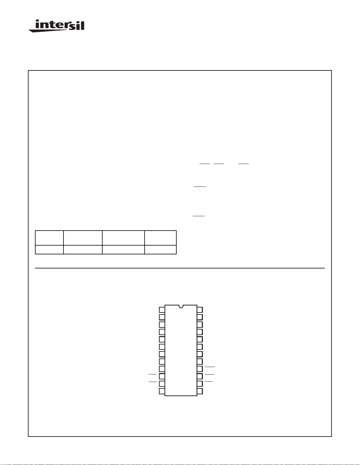
Pinout
CDP1823C/3
(SBDIP)
TOP VIEW
1
BUS 0
2
BUS 1
BUS 2
3
4
BUS 3
5
BUS 4
6
BUS 5
7
BUS 6
BUS 7
8
CS1
9
10
CS2
11
CS3
V
12
SS
CAUTION: These devices are sensitive to electrostatic discharge; follow proper IC Handling Procedures.
http://www.intersil.com or 407-727-9207
| Copyright © Intersil Corporation 1999
6-31
24
V
DD
A0
23
22
A1
A2
21
A3
20
A4
19
A5
18
A6
17
16
MWR
15
MRD
14
CS5
13
CS4
File Number 2982.1

CDP1823C/3
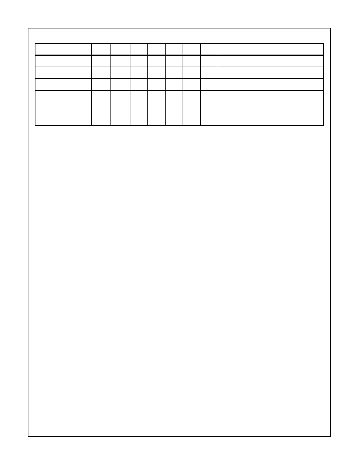
OPERATIONAL MODES
FUNCTION MRD MWR CS1 CS2 CS3 CS4 CS5 BUS TERMINAL STATE
Read 0 X 10010Storage State of Addressed Word
Write 1 0 10010Input High Impedance
Standby 1 1 10010High Impedance
Not Selected X
X
X
X
X
NOTE:
1. Logic 1 = High, Logic 0 = Low, X = Don’t Care.
X
X
X
X
X
0
X
X
X
X
High Impedance
X
1
X
X
X
X
X
1
X
X
X
X
X
0
X
X
X
X
X
1
6-32
 Loading...