6-19
March 1997
CDP1822C/3
High-Reliability CMOS
256-Word x 4-Bit LSI Static RAM
Features
• For Applications in Aerospace, Military, and Critical
Industrial Equipment
• Interfaces Directly with CDP1802 Microprocessor
• Very Low Operating Current
- At V
DD
= 5V and Cycle Time = 1µs . . . . . . 4mA (Typ)
• Static CMOS Silicon-On-Sapphire Circuitry
- CD4000 Series Compatible
• Industry Standard Pinout
• Two Chip Select Inputs - Simple Memory Expansion
• Memory Retention for Standby. . . . . . . . . . . . . 2V (Min)
Battery Voltage
• Single Power Supply Operation . . . . . . . . . . 4V to 6.5V
• High Noise Immunity 30% of V
DD
. . . . . . . . . 4V to 6.5V
• Output Disable for Common I/O Systems
• Three-State Data Output for Bus Oriented Systems
• Separate Data Inputs and Outputs
• Latch-Up-Free Transient Radiation Tolerance
Description
The CDP1822C/3 is a 256 word by 4-bit random access
memory designed for use in memory systems where high
speed, low operating current, and simplicity in use are
desirable. The CDP1822 features high speed and excellent
noise immunity. It has separate data inputs and outputs and
utilizes a single power supply of 4V to 6.5V.
Two Chip Select inputs simplify system expansion. An output
Disable control provides Wire-OR-capability and is also
useful in common Input/Output systems. The Output Disable
input allows this RAM to be used in common data Input/Output systems by forcing the output into a high impedance
state during a write operation independent of the Chip Select
input condition. The output assumes a high impedance state
when the Output Disable is at high level or when the chip is
deselected by
CS1 and/or CS2.
The high noise immunity of the CMOS technology is
preserved in this design. For TTL interfacing at 5V operation,
excellent system noise margin is preserved by using an
external pull-up resistor at each input.
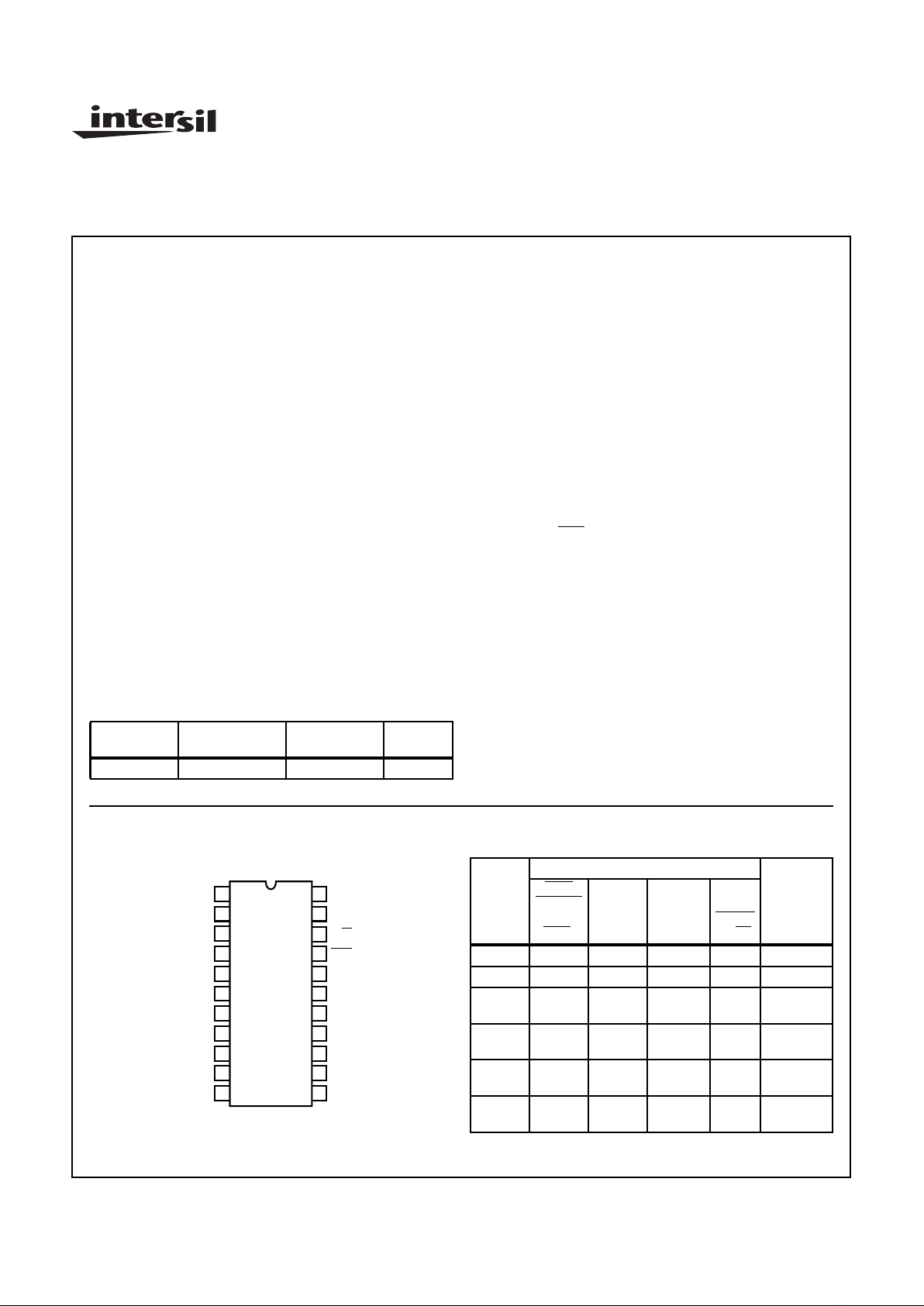
Pinout
CDP1822C/3 (SBDIP)
TOP VIEW
Ordering Information
PACKAGE TEMP. RANGE
PART
NUMBER PKG. NO.
SBDIP -55oC to +125oC CDP1822CD3 D22.4A
1
11
10
9
8
7
6
5
3
2
4
22
12
13
14
15
16
17
18
19
21
20
A2
A1
A0
A5
A6
A7
DI1
V
SS
DO1
DI2
A4
CS1
O. D.
CS2
R/
W
DO4
DI4
DO3
DI3
DO2
A3
V
DD
OPERATIONAL MODES
MODE
INPUTS
OUTPUT
CHIP
SELECT
1
(CS1)
CHIP
SELECT
2
(CS2)
OUTPUT
DISABLE
(OD)
READ/
WRITE
(R/W)
Read 0 1 0 1 Read
Write 0 1 0 0 Data In
Write 0 1 1 0 High
Impedance
Standby 1 X X X High
Impedance
Standby X 0 X X High
Impedance
Output
Disable
X X 1 X High
Impedance
Logic 1 = High, Logic 0 = Low, X = Don’t Care
File Number 2981.1
CAUTION: These devices are sensitive to electrostatic discharge; follow proper IC Handling Procedures.
http://www.intersil.com or 407-727-9207
| Copyright © Intersil Corporation 1999

6-20
Absolute Maximum Ratings Thermal Information
DC Supply Voltage Range, (VDD)
(All Voltages Referenced to VSS Terminal)
CDP1822C/3 . . . . . . . . . . . . . . . . . . . . . . . . . . . . . . -0.5V to +7V
Input Voltage Range, All Inputs . . . . . . . . . . . . .-0.5V to VDD +0.5V
Operating Temperature Range (TA) . . . . . . . . . . . . -55oC to +125oC
Thermal Resistance (Typical) θJA (oC/W) θJC (oC/W)
SBDIP Package. . . . . . . . . . . . . . . . . . 80 21
Maximum Storage Temperature Range (T
STG
) . . .-65oC to +150oC
Maximum Lead Temperature (During Soldering) . . . . . . . . . +265oC
Maximum Junction Temperature. . . . . . . . . . . . . . . . . . . . . .+150oC
Recommended Operating Conditions At T
A
= Full Package Temper ature Range.For maximum reliability, operating conditions
should be selected so that operation is always within the following ranges:
PARAMETER
LIMITS
UNITSMIN MAX
DC Operating Voltage Range 4 6.5 V
Input Voltage Range V
SS
V
DD
V
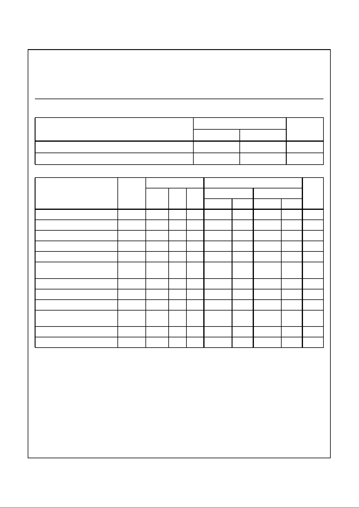
Static Electrical Specifications
PARAMETER SYMBOL
CONDITIONS LIMITS
UNITS
V
O
(V)
V
IN
(V)
V
DD
(V)
-55oC, +25oC +125oC
MIN MAX MIN MAX
Quiescent Device Current (Note 1) I
DD
- 0, 5 5 - 390 - 1000 µA
Output Low (Sink) Current (Note 1) I
OL
0.4 0, 5 5 2.6 - 1.6 - mA
Output High (Source) Current (Note 1) I
OH
4.6 0, 5 5 - -1.2 - -0.8 mA
Output Voltage Low-Level V
OL
- 0, 5 5 - 0.1 - 0.5 V
Output Voltage High-Level V
OH
- 0, 5 5 VDD - 0.1 - VDD - 0.5 - V
Input Low Voltage V
IL
0.5, 4.5 - 5 - 0.3
V
DD
- 0.3
V
DD
V
Input High Voltage V
IH
0.5, 4.5 - 5 0.7 V
DD
- 0.7 V
DD
-V
Input Leakage Current (Note 1) I
IN
- 0, 5 5 - ±3.2 - ±10 µA
Operating Current (Note 1) I
DD1
- 0, 5 5 - 6.5 - 10 mA
Three-State Output Leakage
Current
I
OUT
0, 5 0, 5 5 - ±3.2 - ± 19 µA
Input Capacitance C
IN
- - - - 7.5 - 7.5 pF
Output Capacitance C
OUT
- - - - 7.5 - 7.5 pF
NOTE:
1. Limits designate 100% testing, all other limits are designer’s parameters under given test conditions and do not represent 100% testing.
CDP1822C/3
 Loading...