March 1997
CDP1821C/3
High-Reliability CMOS
1024-Word x 1-Bit Static RAM
Features
• Static CMOS Silicon-On-Sapphire Circuitry CD4000Series Compatible
• Compatible with CDP1800-Series Microprocessors at
Maximum Speed
• Fast Access Time. . . . . . . . . . . 100ns Typ. at V
DD
= 5V
• Single Voltage Supply
• No Precharge or External Clocks Required
• Low Quiescent and Operating Power
• Separate Data Inputs and Outputs
• High Noise Immunity. . . . . . . . . . . . . . . . . . 30% of V
• Memory Retention for Standby Battery Voltage Down
to 2V at +25
o
C
• Latch-Up-Free Transient-Radiation Tolerance
Ordering Information
PART
PACKAGE TEMP. RANGE
SBDIP -55oC to +125oC CDP1821CD3 D16.3
NUMBER PKG. NO.
Description
The CDP1821C/3 is a 1024-word x 1-bit CMOS silicon-on-sapphire (SOS), fully static, random-access memory designed for
use in CDP1800 microprocessor systems. This device has a
recommended operating voltage range of 4V to 6.5V.
The output state of the CDP1821C/3 is a function of the
input address and chip-select states only. Valid data will
appear at the output in one access time following the latest
address change to a selected chip. After valid data appears,
the address may be changed immediately. It is not necessary to clock the chip-select input or any other input terminal
for fully static operation; therefore the chip-select input may
be used as an additional address input. When the device is
in an unselected state (
DD
and output sense amplifier are disabled. This feature allows
the three-state data outputs from many arrays to be OR-tied
to a common bus for easy memory expansion.
CS = 1), the internal write circuitry
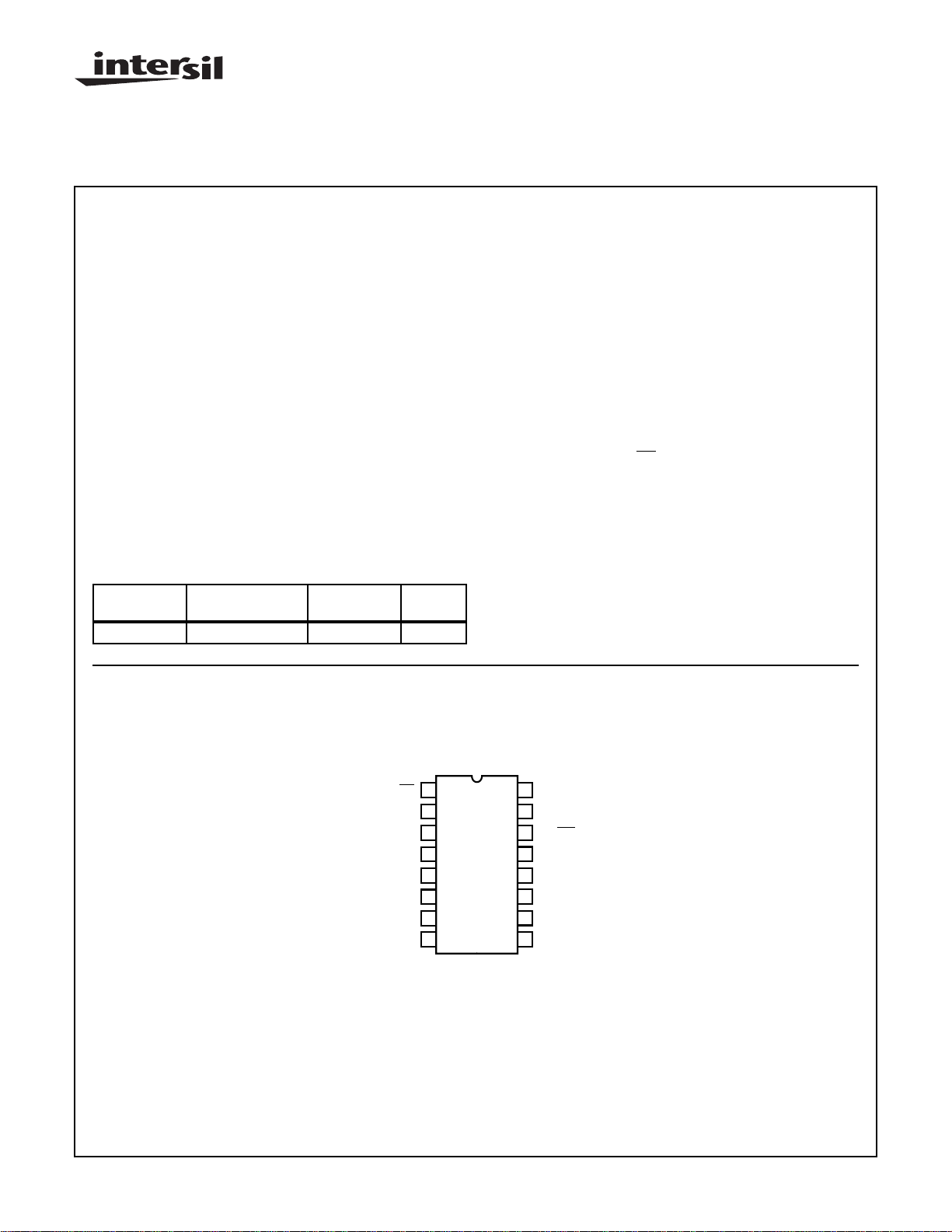
Pinout
CS
A0
A1
A2
A3
A4
DO
V
SS
CDP1821C/3
(SBDIP)
TOP VIEW
1
2
3
4
5
6
7
8
16
15
14
13
12
11
10
9
V
DD
DI
RD/WR
A9
A8
A7
A6
A5
CAUTION: These devices are sensitive to electrostatic discharge; follow proper IC Handling Procedures.
http://www.intersil.com or 407-727-9207
| Copyright © Intersil Corporation 1999
6-5
File Number 2983.1

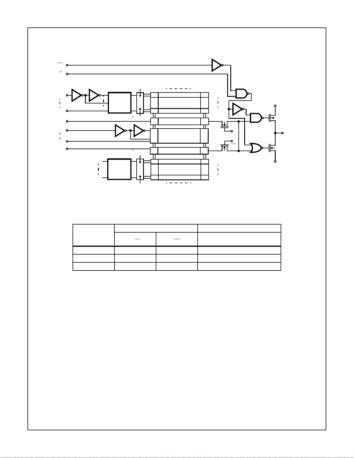
Functional Block Diagram
CS
W
R/
a0
a3
a0
a3
1/16
ROW
DECODER
1/16
ROW
DECODER
A0
A3
DI
A5
A9
DI
ROW
BUFFERS
CS • R/W • A4
CS •
R/W • A4
ROW
BUFFERS
CDP1821C/3
COL. 0 COL. 31
16 x 32
CELL ARRAY
COLUMN BUFFERS
1/32
COLUMN DECODER
COLUMN BUFFERS
16 x 32
CELL ARRAY
COL. 0 COL. 31
ROW 0
ROW 15
ROW 16
ROW 31
A4
A4
V
DD
DO
V
SS
OPERATIONAL MODES
INPUTS OUTPUT
MODE
READ/WRITE
R/W
CHIP-SELECT
CS DATA OUTPUT DO
Standby X 1 High Impedance
Write 0 0 High Impedance
Read 1 0 Contents of Addressed Call
X = Don’t Care Logic 1 = High Logic 0 = Low
6-6

CDP1821C/3
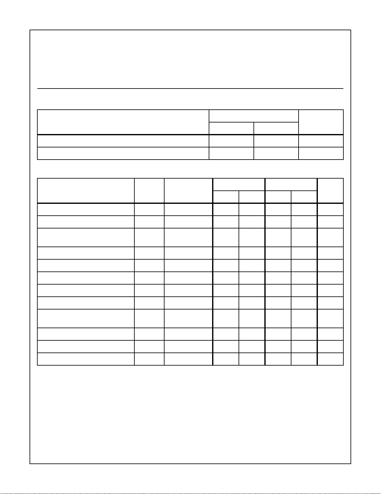
Absolute Maximum Ratings Thermal Information
DC Supply Voltage Range, (VDD)
(All Voltages Referenced to VSS Terminal). . . . . . . . -0.5V to +7V
Input Voltage Range, All Inputs . . . . . . . . . . . . . -0.5V to VDD +0.5V
DC Input Current, Any One Input. . . . . . . . . . . . . . . . . . . . . . . . .±10mA
Thermal Resistance (Typical) θJA (oC/W) θJC (oC/W)
SBDIP Package. . . . . . . . . . . . . . . . . . 75 20
Maximum Operating Temperature Range (TA) . . . .-55oC to +125oC
Maximum Storage Temperature Range (T
Maximum Lead Temperature (During Soldering) . . . . . . . . .+265oC
Maximum Junction Temperature . . . . . . . . . . . . . . . . . . . . . . +150oC
) . . .-65oC to +150oC
STG
Recommended Operating Conditions T
= Full Package-Temperature Range. For maximum reliability, nominal operating con-
A
ditions should be selected so that operation is always within the following ranges:
CDP1821CD/3
PARAMETER
DC Operating Voltage Range 4 6.5 V
Input Voltage Range V
Static Electrical Specifications V
= 5V ±5%
DD
SS
V
DD
-55oC, +25oC +125oC
PARAMETER SYMBOL CONDITIONS
Quiescent Device Current (Note 1) I
Output Low Drive (Sink) Current (Note 1) I
Output High Drive (Source) Current
I
DD
OL
OH
VIN = 0V or V
V
OUT
V
OUT
DD
= 0.4V 2.7 - 1.6 - mA
= VDD -0.4V -1.3 - -0.8 - mA
- 260 - 1000 µA
(Note 1)
Output Voltage Low-Level V
Output Voltage High-Level V
OL
OH
- - 0.1 - 0.5 V
-V
-0.1 - VDD -0.5 - V
DD
UNITSMIN MAX
V
UNITSMIN MAX MIN MAX
Input Low Voltage V
Input High Voltage V
Input Current (Note 1) I
Three-State Output Leakage Current
I
IL
IH
IN
OUT
VIN = 0V or V
VIN = 0V or V
- - 0.3 V
- 0.7 V
DD
DD
DD
- 2.6 - 10 µA
- 2.6 - 10 µA
DD
- 0.7 V
- 0.3 V
DD
DD
V
-V
(Note 1)
Operating Current (Note 2) I
Input Capacitance C
Output Capacitance C
DD1
IN
OUT
- - 5 - 10 mA
- - 7.5 - 7.5 pF
- - 15 - 15 pF
NOTES:
1. Limits designate 100% testing. All other limits are designer’s parameters under given test conditions and do not represent 100% testing
2. Measured with 1µs read-cycle time and outputs floating.
6-7
 Loading...