

查询CDP1805供应商
March 1997
TM
CDP1805AC,
CDP1806AC
CMOS 8-Bit Microprocessor with On-Chip RAM†
and Counter/Timer
Features
• Instruction Time of 3.2µs, -40oC to +85oC
• 123 Instructions - Upwards Software Compatible With
CDP1802
• BCD Arithmetic Instructions
• Low-Power IDLE Mode
• Pin Compatible With CDP1802 Except for Terminal 16
• 64K-Byte Memory Address Capability
• 64 Bytes of On-Chip RAM
• 16 x 16 Matrix of On-Board Registers
• On-Chip Crystal or RC Controlled Oscillator
• 8-Bit Counter/Timer
n
†
Description
The CDP1805AC and CDP1806AC are functional and performance enhancements of the CDP1802 CMOS 8-bit register-oriented microprocessor series and are designed for use
in general-purpose applications.
The CDP1805AC hardware enhancements include a 64byte RAM and an 8-bit presettable down counter. The
Counter/Timer which generates an internal interrupt request,
can be programmed for use in timebase, event-counting,
and pulse-duration measurement applications. The
Counter/Timer underflow output can also be directed to the
Q output terminal. The CDP1806AC hardware enhancements are identical to the CDP1805AC, except the
CDP1806AC contains no on-chip RAM.
The CDP1805AC and CDP1806AC software enhancements
include 32 more instructions than the CDP1802. The 32 new
software instructions add subroutine call and return capability , enh anced data transfe r manip ulatio n, Coun ter/Timer control, improved interrupt handling, single-instruction loop
counting, and BCD arithmetic.
Upwards software and hardware compatibility is maintained
when substituting a CDP1805AC or CDP1806AC for other
CDP1800-series microprocessors. Pinout is identical except
for the replacement of V
the replacement of V
with ME on the CDP1805AC and
CC
with VDD on the CDP1806AC.
CC
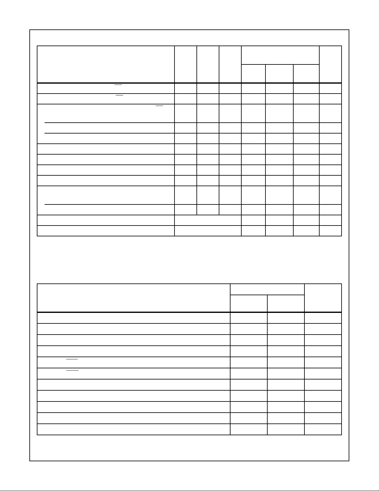
Ordering Information
CDP1805AC CDP1806AC TEMPERATURE RANGE PACKAGE PKG. NO.
o
CDP1805ACE CDP1806ACE -40
- CDP1806ACEX Burn-In
CDP1805ACQ CDP1806ACQ -40
CDP1805ACD CDP1806ACD -40
CDP1805ACDX - Burn-In
† CDP1805AC Only
CAUTION: These devices are sensitive to electrostatic discharge; follow proper IC Handling Procedures.
1-888-INTERSIL or 321-724-7143
Copyright © Intersil Americas Inc. 2002. All Rights Reserved
| Intersil (and design) is a trademark of Intersil Americas Inc.
C to +85oC Plastic DIP E40.6
o
C to +85oC PLCC N44.65
o
C to +85oC SBDIP D40.6
1
File Number 1370.2
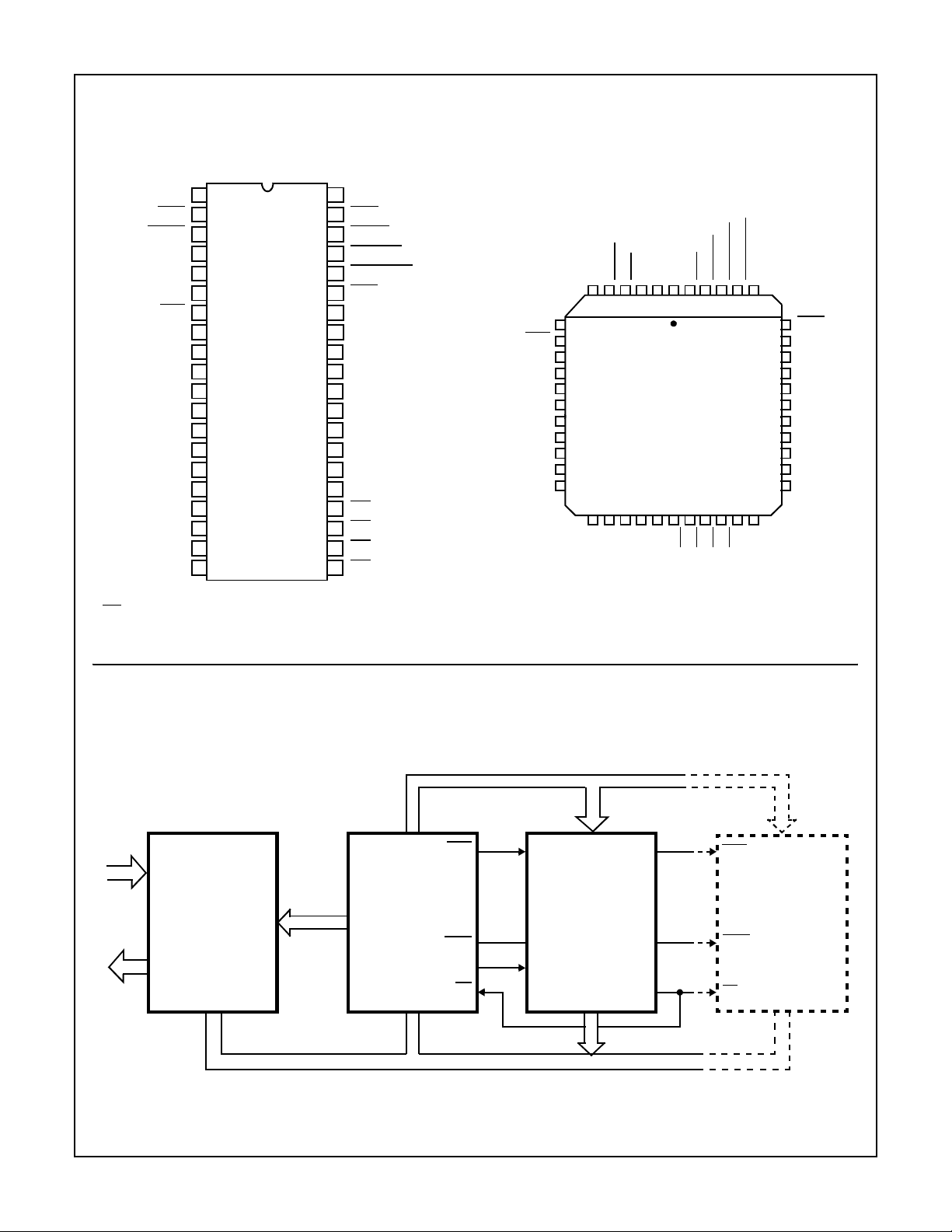
Pinouts
CDP1805AC, CDP1806AC
(PDIP, SBDIP)
TOP VIEW
CDP1805AC, CDP1806AC
CDP1805AC, CDP1806AC
(PLCC, PACKAGE TYPE Q)
TOP VIEW
† ME
for CDP1805AC
for CDP1806AC
V
DD
CLOCK
WAIT
CLEAR
SC1
SC0
MRD
BUS 7
BUS 6
BUS 5
BUS 4
BUS 3
BUS 2
BUS 1
BUS 0
N2
N1
N0
V
SS
1
2
3
4
Q
5
6
7
8
9
10
11
12
13
14
15
†
16
17
18
19
20
V
40
XTAL
39
38
DMA IN
37
DMA OUT
36
INTERRUPT
35
MWR
TPA
34
TPB
33
MA7
32
MA6
31
MA5
30
MA4
29
MA3
28
MA2
27
MA1
26
MA0
25
EF1
24
23
EF2
22
EF3
21
EF4
DD
SC0
MRD
BUS 7
BUS 6
BUS 5
NC
BUS 4
BUS 3
BUS 2
BUS 1
BUS 0
7
8
9
10
11
12
13
14
15
16
17
SC1QCLEAR
20 21 22 23 24 25 261918
†
N2N1N0
WAIT
CLOCKNCVDDXTAL
123456
SS
NC
V
DMA - IN
DMA - OUT
44 43 42 41 40
EF3
EF2
EF4
EF1
INTERRUPT
39
38
37
36
35
34
33
32
31
30
29
2827
MA0
MWR
TPA
TPB
MA7
MA6
NC
MA5
MA4
MA3
MA2
MA1
Schematic
IN
OUT
CDP1851
PIO
BUS0 - BUS7
FIGURE 1. TYPICAL CDP1805AC, CDP1806AC SMALL MICROPROCESSOR SYSTEM
CONTROL
MA0 - MA7
CDP1805AC WITH
RAM, COUNTER/TIMER
CDP1806AC WITH
COUNTER/TIMER
BUS0 - BUS7
MRD
MWR
TPA
ME
TPA
(CDP1805AC ONLY)
8-BIT DATA BUS
ADDRESS BUS
MA0 - MA7
CDP1833
1K BYTE ROM
BUS0 - BUS7
CEO
MA0-MA4
MRD
CDP1824
32 BYTE RAM
(USED WITH
CDP1806AC ONLY)
MWR
CS
BUS0-BUS4
2
CLOCK
CDP1805AC, CDP1806AC
STATE
CODES
SYSTEM
TIMING
XTAL
SCO
SCI
Q LOGIC
TPA
TPB
MWR
MRD
I/O
COMMANDS
N0N1N2
N
(4)
WAIT
CONTROL
CLEAR
INTIN
OUT
DMA
DMA
I/O REQUESTS
EF4
EF3
EF2
I/O FLAGS
EF1
MA0
MA1
MA2
MA3
MA4
MA5
MA6
MA7
MEMORY ADDRESS LINES
LOGIC
CLOCK
TIMING LOGIC
CONTROL AND
EF1
MUX
TC
DECODE
INSTRUCTION
INTERRUPT
EF2
TPA
LOGIC
ARRAY
REGISTER
A
(16)
÷ 32
INCR/
DF
DECR
(1)
MODE
CONTROL
CLK
I
(4)
P
(4)
T
(8)
X
(4)
AND
LATCH
R(2).0
R(2).1
DECODE
R(9).0
R(A).0
R(9).1
R(A).1
R(F).0
R(E).0
R(F).1
R(E).1
8-BIT BIDIRECTIONAL DATA BUS
R
R(0).0
R(1).0
R(0).1
R(1).1
ALU
8-BIT
COUNTER/TIMER
B
D
(8)
(8)
BUS 0
BUS 1
BUS 2
BUS 3
BUS 4
ME FOR CDP1805AC
FOR CDP1806AC
DD
V
CDP1805AC
RAM
64-BYTE
ONLY
REGISTER (CH)
COUNTER HOLDING
FIGURE 2. BLOCK DIAGRAM FOR CDP1805AC AND CDP1806AC
3
BUS 5
BUS 6
BUS 7
CDP1805AC, CDP1806AC
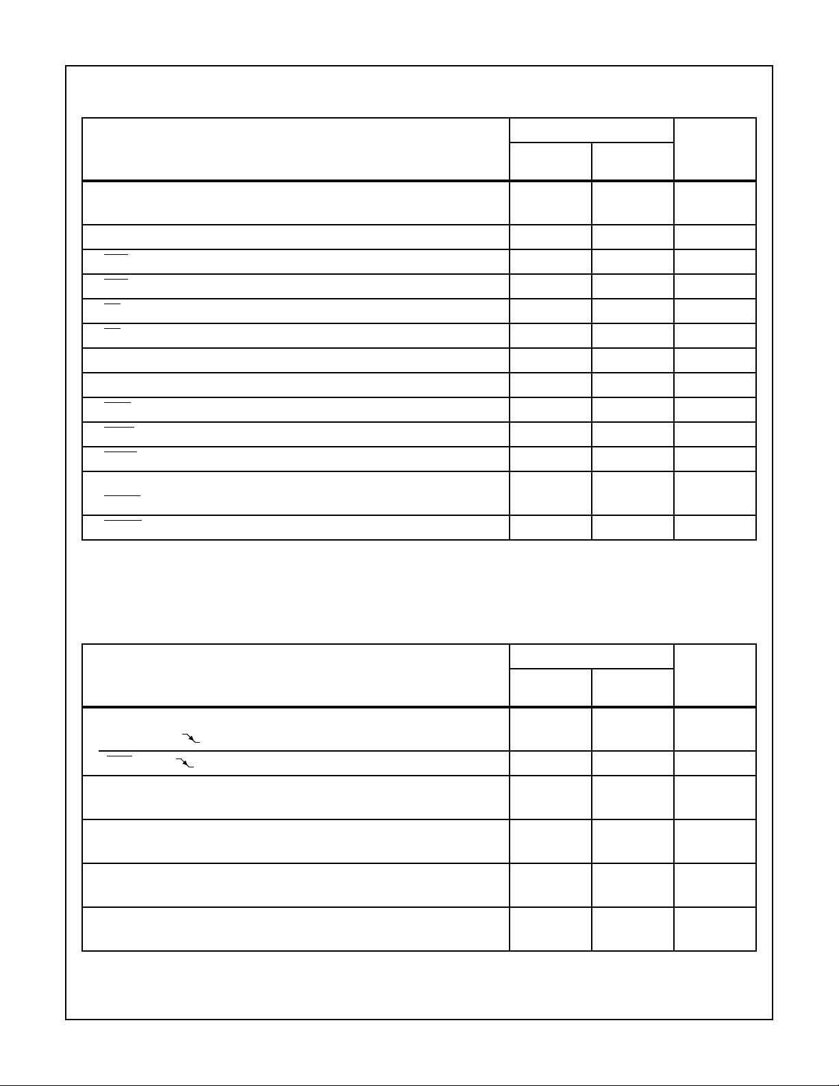
Absolute Maximum Ratings Thermal Information
DC Supply Voltage Range, (VDD)
(All Voltages Referenced to V
Input Voltage Range, All Inputs . . . . . . . . . . . . .-0.5V to V
DC Input Current, any One Input. . . . . . . . . . . . . . . . . . . . . . . . .± 10mA
Terminal). . . . . . . . . -0.5V to +7V
SS
DD
+0.5V
Thermal Resistance (Typical, Note 2) θ
PDIP Package. . . . . . . . . . . . . . . . . . . 50 N/A
PLCC Package . . . . . . . . . . . . . . . . . . 46 N/A
SBDIP Package. . . . . . . . . . . . . . . . . . 55 15
Device Dissipation Per Output Transistor
= Full Package Temperature Range . . . . . . . . . . . . . . 100mW
T
A
Operating Temperature Range (T
Package Type D . . . . . . . . . . . . . . . . . . . . . . . . .-55
)
A
Package Type E and Q . . . . . . . . . . . . . . . . . . . . .-40
Storage Temperature Range (T
Lead Temperature (During Soldering)
). . . . . . . . . . . .-65oC to +150oC
STG
At Distance 1/16 ±1/32in (1.59 ± 0.79mm) from case for
10s Max. . . . . . . . . . . . . . . . . . . . . . . . . . . . . . . . . . . . . .+265
Printed Circuit Board Mount: 57mm x 57mm Minimum Area x 1.6mm
Thick G10 Epoxy Glass, or Equivalent.
CAUTION: Stresses above t hos e l iste d in “Absolute Maxi mum Ra ti ng s” m ay cau se per ma nent damage to the d evice . T his is a stress only rating and operati on
of the device at these or any other conditions above those in dica ted in the operational sections of this specification is not implied.
(oC/W) θJC (oC/W)
JA
o
C to +125oC
o
C to +85oC
o
C
Recommended Operating Conditions T
= Full-Package Temperature Range. For maximum reliability, operating conditions
A
should be selected so that operation is always within the following ranges.
CDP1805ACD, CDP1805ACE
PARAMETER
TEST CONDITIONS
V
DD
(V)
CDP1806ACD, CDP1806ACE
UNITSMIN MAX
DC Operating Voltage Range - 4 6.5 V
Input Voltage Range - V
Minimum Instruction Time (Note 1)
(f
= 5MHz)
CL
53.2-µs
SS
V
DD
V
Maximum DMA Transfer Rate 5 - 0.625 Mbyte/s
Maximum Clock Input Frequency,
Load Capacitance (C
) = 50pF
L
Maximum External Counter/Timer Clock
Input Frequency to EF1
, EF2
5DC5MHz
5DC2MHz
NOTES:
1. Equals 2 machine cycles - one Fetch and one Execute operation for all instructions except Long Branch, Long Skip, NOP, and “68” family
instructions, which are more than two cycles.
is measured with the component mounted on an evaluation PC board in free air.
2. θ
JA
Static Electrical Specifications at T
= -40oC to +85oC, VDD ±5%, Except as Noted
A
CDP1805ACD, CDP1805ACE
CDP1806ACD, CDP1806ACE
PARAMETER
Quiescent Device Current, I
Output Low Drive (Sink) Current, (Except XTAL
Output, I
XTAL
OL
DD
), I
Output High Drive (Source) Current (Except XTAL
XTAL
, I
OH
Output Voltage Low Level, V
Output Voltage High Level, V
OL
OH
OL
, I
OH
V
(V)
V
O
(V)
V
IN
DD
(V)
(NOTE 3)
TYP MAX
UNITSMIN
- 0, 5 5 - 50 200 µA
0.4 0, 5 5 1.6 4 - mA
0.4 5 5 0.2 0.4 - mA
4.6 0, 5 5 -1.6 -4 - mA
4.6 0 5 -0.1 -0.2 - mA
-0, 55 - 0 0.1 V
-0, 554.9 5 - V
4
CDP1805AC, CDP1806AC
Static Electrical Specifications at T
= -40oC to +85oC, VDD ±5%, Except as Noted (Continued)
A
CDP1805ACD, CDP1805ACE
CDP1806ACD, CDP1806ACE
PARAMETER
Input Low Voltage (BUS0 - BUS7, ME), V
Input High Voltage (BUS0 - BUS7, ME
), V
IL
IH
Schmitt Trigger Input Voltage (Except BUS0 - BUS7, ME
Positive Trigger Threshold, V
Negative Trigger Threshold, V
Hysteresis, V
H
Input Leakage Current, I
Three-State Output Leakage Current, I
Input Capacitance, C
Output Capacitance, C
IN
OUT
P
N
IN
OUT
V
(V)
0.5, 4.5 - 5 - - 1.5 V
0.5, 4.5 - 5 3.5 - - V
)
0.5, 4.5 - 5 2.2 2.9 3.6 V
0.5, 4.5 - 5 0.9 1.9 2.8 V
0.5, 4.5 - 5 0.3 0.9 1.6 V
-0, 55 - ±0.1 ±5 µA
0, 5 0, 5 5 - ±0. 2 ±5 µA
---- 5 7.5pF
---- 10 15pF
V
O
(V)
V
IN
DD
(V)
(NOTE 3)
TYP MAX
Total Power Dissipation (Note 4)
Run - - 5 - 35 50 mW
Idle “00” at M (0000) - - 5 - 12 18 mW
UNITSMIN
Minimum Data Retention Voltage, V
Data Retention Current, I
DR
DR
NOTES:
3. Typical values are for T
4. External clock: f = 5MHz, t
= +25oC and nominal VDD.
A
, tF = 10ns; CL = 50pF.
R
Dynamic Electrical Specifications at T
V
PARAMETER
Propagation Delay Times
Clock to TPA, TPB, t
Clock-to-Memory High-Address Byte, t
Clock-to-Memory Low-Address Byte, t
Clock to MRD
Clock to MWR
, t
PLH
, t
PLH
Clock to (CPU DATA to BUS), t
Clock to State Code, t
Clock to Q, t
Clock to N, t
PLH
PLH
, t
, t
Clock to Internal RAM Data to BUS, t
, t
PLH
PHL
, t
PLH
PHL
, t
PLH
PHL
, t
PHL
, t
(See Note 5) 150 275 ns
PHL
, t
PLH
PHL
, t
PLH
PHL
PHL
PHL
, t
PLH
PHL
VDD = V
DR
-22.4V
VDD = 2.4 - 25 100 µA
= -40o to +85oC; CL = 50pF; Input tR, tF = 10ns; Input Pulse Levels = 0.1V to
A
-0.1V; VDD = 5V, ±5%.
DD
CDP1805AC CDP1806AC
(NOTE 5)
TYP MAX
150 275 ns
325 550 ns
275 450 ns
200 325 ns
375 625 ns
225 400 ns
250 425 ns
250 425 ns
420 650 ns
UNITS
5
CDP1805AC, CDP1806AC
Dynamic Electrical Specifications at T
= -40o to +85oC; CL = 50pF; Input tR, tF = 10ns; Input Pulse Levels = 0.1V to
A
-0.1V; VDD = 5V, ±5%. (Continued)
V
DD
PARAMETER
Minimum Set-Up And Hold Times (Note 2)
Data Bus Input Set-Up, t
Data Bus Input Hold, t
DMA
DMA
ME
Set-Up, t
ME
Hold, t
Set-Up, t
Hold, t
SU
H
SU
H
Interrupt Set-Up, t
Interrupt Hold, t
WAIT
Set-Up, t
EF1-4
Set-Up, t
EF1 -4
Hold, t
H
SU
SU
H
SU
H
SU
Minimum Pulse Width Times (Note 6)
CLEAR
CLOCK
Pulse Width, t
Pulse Width, t
WL
W
NOTES:
5. Typical values are for T
= 25o C and nominal V
A
DD
.
6. Maximum limits of minimum characteristics are the values above which all devices function.
CDP1805AC CDP1806AC
(NOTE 5)
TYP MAX
UNITS
-100 0 ns
125 225 ns
-75 0 ns
100 175 ns
125 320 ns
050ns
-100 0 ns
100 175 ns
20 50 ns
-125 0 ns
175 300 ns
100 175 ns
75 100 ns
Timing Specifications as a function of T (T =
1
/f
) at TA = -40 to +85oC, VDD = 5V, ±15%
CLOCK
CDP1805AC, CDP1806AC
(NOTE 7)
PARAMETER
MAX
High-Order Memory-Address Byte
Set-Up to TPA Time, t
MRD
to TPA Time, t
SU
SU
2T-275 2T -175 ns
T/2 -100 T/2 -75 ns
High-Order Memory-Address Byte
Hold after TPA Time, t
H
T/2 +75 T/2 +100 ns
Low-Order Memory-Address Byte
Hold after WR Time, t
H
T +180 T +240 ns
CPU Data to Bus
Hold after WR Ti me, t
H
Required Memory Access Time, t
ACC
T +110 T +150 ns
Address to Data 4.5T -440 4.5T -330 ns
NOTE:
7. Typical values are for T
= +25oC and nominal VDD.
A
UNITSTYP
6
CDP1805AC, CDP1806AC
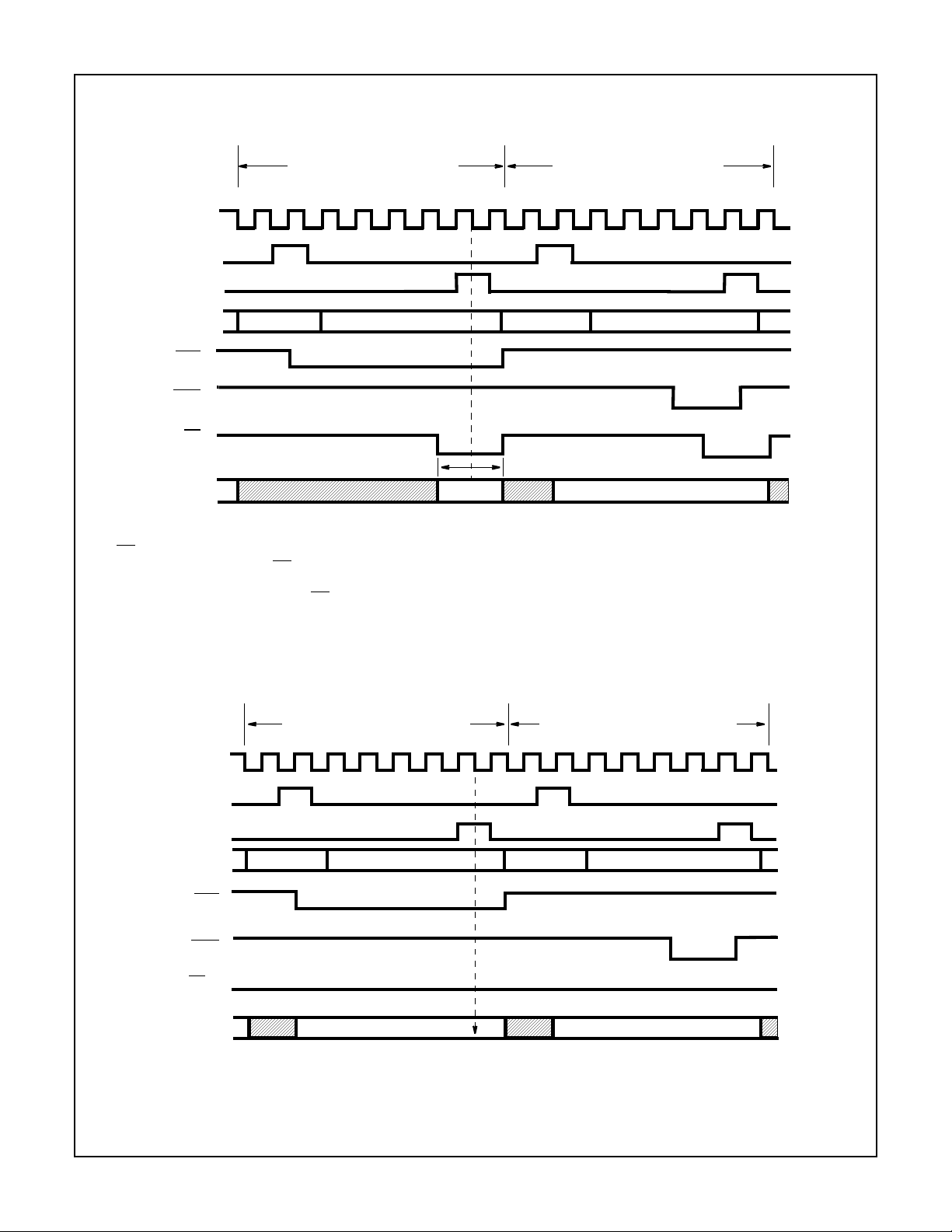
Timing Waveforms For Possible Operating Modes
INTERNAL RAM READ CYCLE INTERNAL RAM WRITE CYCLE
00 10 20 30 40 50 60 70 00 10 20 30 40 50 60 70
CLOCK
01 11 21 31 41 51 61 71 01 11 21 31 41 51 61 71
TPA
TPB
MEMORY
ADDRESS
MRD
MWR
†ME
DATA
BUS
IN
HIGH BYTE LOW BYTE HIGH BYTE LOW BYTE
VALID DATA FROM MEMORY
VALID DATA FROM CPU
NOTE:
has a minimum setup and hold time with respect to the beginning of clock 70. For a memory read operation, RAM data will appear on
8. ME
the data bus during the time ME
is active after clock 31. The time shown can be longer, if for instance, a DMA out operation is performed
on internal RAM data, to allow data enough time to be latched into an external device. The internal RAM is automatically deselected at
the end of clock 71 independent of ME
.
† For CDP1805AC only.
FIGURE 3. INTERNAL MEMORY OPERATION TIMING WAVEFORMS
EXTERNAL MEMORY READ CYCLE EXTERNAL MEMORY WRITE CYCLE
00 10 20 30 40 50 60 70 00 10 20 30 40 50 60 70
CLOCK
TPA
01 11 21 31 41 51 61 71 01 11 21 31 41 51 61 71
TPB
MEMORY
ADDRESS
MRD
MWR
†ME IN
(HIGH)
DATA
BUS
NOTE:
† For CDP1805AC only.
HIGH BYTE LOW BYTE LOW BYTEHIGH BYTE
DATA LATCHED IN CPU VALID DATA FROM CPU
FIGURE 4. EXTERNAL MEMORY OPERATION TIMING W AVEFORMS
7
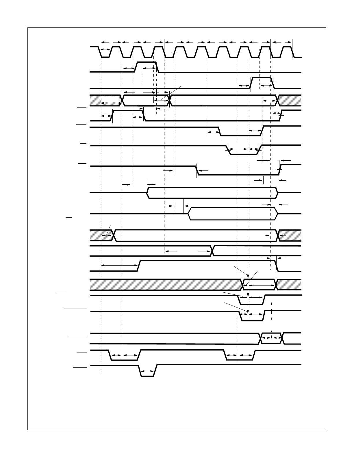
CDP1805AC, CDP1806AC
CLOCK
TPA
TPB
MEMORY
ADDRESS
MRD
(MEMORY
READ CYCLE)
MWR
(MEMORY
WRITE CYCLE)
† ME
(MEMORY
ENABLE)
†† EMS
(EXTERNAL
MEMORY
SELECT)
DATA FROM
CPU TO BUS
DATA FROM
INTERNAL MEMORY
TO BUS (ME
= LOW)
t
W
1 2 3 4 5 6 7 0
00 01 10 11 20 21 30 31 40 41 50 51 60 61 70071 00 01
t
PLH, tPHL
t
PLH
t
PLH,
t
PHL
t
PLH
HIGH ORDER
ADDRESS BYTE
t
PLH,
t
t
SU
PHL
t
t
PHL
t
SU
PHL
t
t
PLH, tPHL
t
H
LOW ORDER
ADDRESS BYTE
t
IS ALLOWABLE
SU
INTERNAL RAM
ACCESS TIME
t
PLH
t
PHL
t
PHL
t
PHL
PLH
t
SU
t
PLH
t
PLH
t
t
PHL
t
H
t
PHL
H
t
H
t
PLH, tPLH
t
SUtH
t
PLH, tPHL
t
SU
t
H
t
t
SU
H
t
t
SU
H
SAMPLED END OF S0
FLAG LINES
t
SUtH
STATE CODES
N0, N1, N2
(I/O EXECUTION
CYCLE)
DATA FROM
BUS TO CPU
DMA REQUEST
INTERRUPT
REQUEST
EF1 - EF4
Q
t
PLH
t
PLH, tPHL
DATA LATCHED
IN CPU
DMA SAMPLED (S1, S2, S3)
INTERRUPT
SAMPLED (S1, S2)
t
SUtH
WAIT
t
CLEAR
WL
NOTES:
† This Timing Diagram is used to show signal relationships only, and does not represent any specific machine cycle.
† All measurements are referenced to 50% point of the wave forms.
† Shaded areas indicate “don’t care” or undefined state. Multiple transitions may occur during this period.
† For the run (RAM only) mode only.
†† For the run (RAM/ROM) mode only.
FIGURE 5. TIMING WAVEFORMS
t
PHL
8
CDP1805AC, CDP1806AC
Enhanced CDP1805AC and CDP1806AC
Operation
MRD
= VDD: Input data from I/O to CPU and memory.
MRD
= VSS: Output data from Memory to I/O.
Timing
Timing for th e CDP1 805 AC and C DP 18 06AC is the sa me as
the CDP1802 microprocessor series, with the following
exceptions:
• 4.5 Clock Cycles Are Provided for Mem ory Access Instea d
of 5.
• Q Changes 1/2 Clock Cycle Earlier During the SEQ and
REQ Instructions.
• Flag Lines (EF1
-EF4) Are Sampled at the End of the S0
Cycle Instead of at the Beginning of the S1 Cycle.
• Pause Can Only Occur on the Low-To-High Transition of
Either TPA or TPB, Instead of any Negative Clock Transition.
Special Features
Schmitt triggers are provided on all inputs, except ME
and
BUS 0-BUS 7, for maximum immunity from noise and slow
signal transitions. A Schmitt Trigger in the oscillator section
allows ope ration with an RC or crystal.
The CDP1802 Series LOAD mode is not retained. This
mode (WAIT
, CLEAR = 0) is not allowed on the CD P180 5AC
and CDP1806AC.
A low power mode is provided, whic h is initi ated via the ID LE
instruction. In th is m ode all external sig na ls, except the osci llator, are stopped on the low-to-high transition of TPB. All
outputs remain in their previous states, MRD
is set to a logic
“1”, and the data bus floats. The IDLE mode is exited by a
DMA or INT condition. The INT includes both external interrupts and interrupts generated by the Counter/Timer. The
only restrictions are that the Timer mode, which uses the
TPA ÷ 32 clock source, and the underflow condition of the
Pulse Width Measurement modes are not available to exit
the IDLE mode.
EF1
to EF4 (4 Flags)
These inputs enable the I/O controllers to transfer status
information to the processor. The levels can be tested by the
conditional branch instructions. They can be used in conjunction with the INTERRUPT request line to establish interrupt priorities. The flag(s) are sampled a t the end of every S0
cycle. EF1 and EF2 are also used for event counting and
pulse width measurement in conjunction with the
Counter/Timer.
INTERRUPT
DMA-lN
S2, and S3 cycle. INTERRUPT
, DMA-IN, DMA-OUT (3 I/O Requests)
and DMA-OUT are sampled duri ng TPB every S1 ,
is sampled during TPB e ver y
S1 and S2 cycle.
Interrupt Action - X and P are stored in T after executing
current instruction; designator X is set to 2; designator P is
set to 1; interrupt enable (MIE) is reset to 0 (inhibit); and
instruction execution is resumed. The interrupt action
requires one machine cycle (S3).
DMA Action - Finish executing current instruction; R(0)
points to memory area for data transfer; data is loaded into
or read out of memory; and R(0) is incremented.
NOTE: In the event of concurrent DMA and INTERRUPT requests,
DMA-IN has priority followed by DMA-OUT and then INTERRUPT.
(The interrupt request is not internally latched and must be held true
after DMA).
SC0, SC1, (2 State Code Lines)
These outputs indicate that the CPU is: 1) fetching an
instructio n, o r 2 ) e x ec uti ng a n i ns tr uc t ion, or 3) pr oce s si ng a
DMA request, or 4) acknowledging an interrupt request. The
levels of state code are tabulated below. All states are valid
at TPA.
STATE CODE LINES
Signal Descriptions
Bus 0 to Bus 7 (Data Bus)
8-Bit bidirectional DATA BUS lines. These lines are used for
transferring data between the memory, the microprocessor,
and I/O devices.
N0 to N2 (I/O) Lines
Activated by an I/O instruction to signal the I/O control logic
of a data transfer between memory and I/O interface. These
lines can be used to issue command codes or device selection codes to the I/O devices. The N-bits are low at all times
except when an I/O instruction is being executed. During this
time their state is the same as the corresponding bits in the
N Register. The direction of data flow is defined in the I/O
instruction by bit N3 (internally) and is indicated by the level
of the MRD
Signal:
STATE TYPE
S0 (Fetch) L L
S1 (Execute) L H
S2 (DMA) H L
S3 (Interrupt) H H
NOTE: H = V
DD
, L = V
SS.
SC1 SC0
TPA, TPB (2 Timing Pulses)
Positive pulses that occurrence in each machine cycle (TPB
follows TPA). They ar e used by I/O controll ers to interpret
codes and to time interaction with the data bus. The trailing
edge of TPA is used by the memo ry syst em to latch th e highorder byte of the multiplexed 16-bit memory address.
9

MA0 to MA7 (8 Memory Address Lines)
CDP1805AC, CDP1806AC
ME
(Memory Enable CDP1805AC Only)
In each cycle, the higher-order byte of a 16-bit memory
address appears on the memory address lines MA0-7 first.
Those bits required by the memory system can be strobed
into external address latches by timing pulse TPA. The loworder byte of the 16-bit address appears on the address
lines 1/2 clock after the termination of TPA.
(Write Pulse)
MWR
A negative pulse appearing in a memory-write cycle, after
the address lines have stabilized.
(Read Level)
MRD
A low level on MRD indicates a memory read cycle. It can be
used to control three-st at e output s from the add ressed memory and to indicate th e direct ion of dat a transf er during an I/O
instruction.
Q
Single bit output from the CPU which can be set or reset,
under program control. During SEQ and REQ instruction
execution, Q is set or reset between the trailing edge of TPA
and the leading edge of TPB. The Q line can also be controlled by the Coun ter/Timer underf low via the Enable Toggle
Q instruction.
The Enable Toggle Q command connects the Q-line flip-flop
to the output of the counter, such that each time the counter
decrements from 01 to its next value, the Q line changes
state. This command is cleared by a LOAD COUNTER
(LDC) instruction with the Counter/Timer stopped, a CPU
reset, or a BRANCH COUNTER INTERRUPT (BCl) instruction with the counter interrupt flip-flop set.
Clock
Input for externally generated single-phase clock. The maximum clock frequency is 5MHz at V
= 5V. The clock is
DD
counted down internally to 8 clock pulse s pe r machine cycle.
XTAL
Connection to be u se d with clock input terminal, for an external crystal, if the on-chip oscillator is utilized.
This active low input is used to selec t or d es ele ct the internal
RAM. It must be active prior to clock 70 for an internal RAM
access to take place. Intern al RAM data will appear on the
data bus during the time that ME is active (after clock 31).
Thus, if this dat a is to be l atc hed int o an ex tern al d evi ce (i.e.,
during an OUTPUT instruction or DMA OUT cycle), ME
should be wide enough to provide enough time for valid data
to be latched. The internal RAM is automatically deselected
after clock 71. ME is ineffective when MRD • MWR = 1.
The internal RAM is not internally mask-decoded. Decoding
of the starting address is performed externally, and may
reside in any 64-byte block of memory.
VDD (CDP1806AC Only)
This input replaces the ME signal of the CDP1805AC and
must be connected to the positive power supply.
, VSS, (Power Levels)
V
DD
VSS is the most negative supply voltage terminal and is normally connected to ground. V
age terminal. All outputs swing from V
recommended input voltage swing is from V
is the positive supply volt-
DD
SS
SS
to V
to VDD.
DD
. The
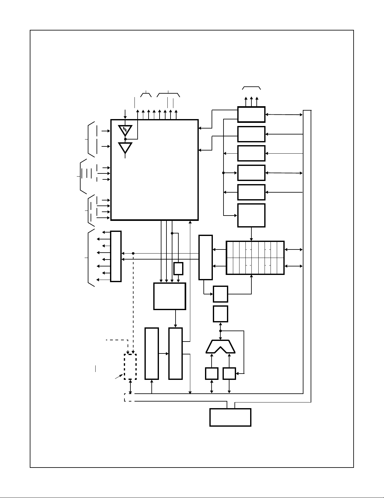
Architecture
Figure 2 shows a block diagram of the CDP1805AC and
CDP1806AC. The principal feature of this system is a register array (R) consisting of sixteen 16-bit scratchpad registers. Individual registers in the array (R) are designated
(selected) by a 4-bit binary code from one of the 4-bit registers labeled N, P, and X. The contents of any register can be
directed to any one of the following paths:
1. The external memory (multiplexed, higher-order byte first
on to 8 memory address lines).
2. The D register (either of the two byt es c an be gat ed to D ).
3. The increment/decrement circuit where it is increased or
decreased by one and stored back in the selected 16-bit
register.
4. To any other 16-bit scratch pad reg ister in the array.
, CLEAR (2 Control Lines)
WAIT
Provide four control modes as listed in the following truth
table:
CLEAR WAIT MODE
L L Not Allowed
L H Reset
H L Pause
HHRun
The four paths, depending on the nature of the instruction,
may operate independently or in various combinations in the
same machine cycle.
Most instructions consist of two 8-clock-pulse machine
cycles. The first cycle is the fetch cycle, and the sec on d, an d
more if necessary, are execute cycles. During the fetch cy cl e
the four bits in the P design ator select one of the 16 register s
R(P) as the current program counter. The selected register
R(P) contains the address of the memory location from
which the instruction is to be f etched . When the instruction is
read out from the memory, the higher order 4 bits of the
instruction byte are loaded into the register and the lower
order 4 bits into the N register. The content of the program
counter is automatically incremented by one so that R(P) is
now “pointing” to the next byte in the memory.
10

CDP1805AC, CDP1806AC
The X designator selects one of the 16 registers R(X) to
“point” to the memory fo r an o pera nd (or d at a ) i n cert a in ALU
or I/O operations.
The N designator can perform the following five functions
depending on the type of instruct ion fetche d:
1. Designate one of the 16 registers in R to be acted upon
during register operations.
2. Indicate to the I/O devices a command code or deviceselection code for peripherals.
3. Indicate the specific operation to be executed during the
ALU instructions, types of tests to be performed during
the Branch instructions, or the specific operation required
in a class of miscellaneous instructions.
4. Indicate the value to be loaded into P to designate a new
register to be used as the program counter R(P).
5. Indicate the value to be loaded into X to designate a new
register to be used as data pointer R(X).
The registers in R can be as sign ed by a p rogramm er in thre e
different ways as program counters, as data pointers, or as
scratchpad locations (data registers) to hold two bytes of
data.
Program Counters
Any register can be the main program counter; the address
of the selected regi ster is held in the P desi gnator. Other registers in R can be used as subroutine program counters. By
a single instruction the contents of the P register can be
changed to effect a “cal l” to subrou tine . Whe n int errupts are
being serviced, register R(1) is used as the program counter
for the user's interrupt servicing routine. After reset, and during a DMA operation, R(0) is used as the program counter.
At all other times the register desi gn ated a s p r og ram co un ter
is at the discretion of the user.
Data Pointers
The registers in R may be used as dat a pointe rs to indica te a
location in memory. The register designated by X (i.e., R(X))
points to memory for the following instructions (see Table 1):
1. ALU operations.
2. Output instructions.
3. Input instructions.
4. Register to memory transfer.
5. Memory to register transfer.
6. Interrupt and subroutine handling.
The register designated by N (i.e., R(N)) points to memory
for the “load D from memory” instructions ON and 4N and
the “Store D” instruction 5N. The register designated by P
(i.e., the program counter) is used as the data pointer for
ALU instructions F8-FD, FF, 7C, 7D, 7F, and the RLDl
instruction 68CN. During these instruction executions, the
operation is referred to as “data immediate”.
Another important use of R as a data pointer supports the
built-in Direct-Memory-Access (DMA) function. When a
DMA-ln or DMA-Out request is received, one machine cycle
is “stolen”. This operation occurs at the end of the execute
machine cycle in the current instruction. Register R(0) is
always used as the data pointer during the DMA operation.
The data is read from (DM A-O ut) o r w ritte n i nto (DMA-l n) th e
memory location pointed to by the R(0) register. At the end
of the trans fer, R(0) is increment ed by one so that the processor is ready to act upon the next DMA byte transfer
request. This feature in the CDP1805AC and CDP1806AC
architecture saves a substantial amount of logic when fast
exchanges of blocks of data are required, such as with magnetic discs or during CRT-display-refre sh cycles.
Data Registers
When registers in R are used to store bytes of data, instructions are provided which allow D to receive from or write into
either the higher-order- or lower-order-byte portions of the
register designated by N. By this mechanism (together with
loading by dat a im me dia te) program pointer a nd d at a pointer
designations are initialized. Also, this technique allows
scratchpad registers in R to be used to hold general data. By
employing in crement or decr ement instructi ons, such regi sters may be used as loop counters. The new RLDl, RLXA,
RSXD, and RNX instructions also allow loading, storing, and
exchanging the full 16-Bit contents of the R registers without
affecting the D register. The new DBNZ instruction allows
decrementing and branching-on-not-zero of any 16-Bit R
register also without affecting the D register.
The Q Flip-Flop
An internal flip-flop, Q, can be set or reset by instruction and
can be sensed by conditional branch instructions. It can also
be driven by the underfl ow output of th e counter/timer The
output of Q is also available as a microprocessor output.
REGISTER SUMMAR Y
D 8 Bits Data Register (Accumulator)
DF 1-Bit Data Flag (ALU Carry)
B 8 Bits Auxiliary Holding Register
R 16 Bits 1 of 16 Scratch and Registers
P 4 Bits Designates which Register is Program
Counter
X 4 Bits Designates which Register is Data Pointer
N 4 Bits Holds Low-Order Instr. Digit
I 4 Bits Holds High-Order Instr. Digit
T 8 Bits Holds old X, P after Interrupt (X is high nibble)
Q 1-Bit Output Flip-Flop
CNTR 8-Bits Counter/Timer
CH 8 Bits Holds Counter Jam Value
MIE 1-Bit Master Interrupt Enable
ClE 1-Bit Counter Interrupt Enable
XlE 1-Bit External Interrupt Enable
ClL 1-Bit Counter Interrupt Latch
11

CDP1805AC, CDP1806AC
Interrupt Servicing
Register R(1) is always used as the program counter whenever interrupt servicing is initialized. When an interrupt
request occurs and the interrupt is allowed by the program
(again, nothing takes place until the completion of the current instruction), the contents of the X and P registers are
stored in the temporary Register T, and X and P are set to
new values; hex digi t 2 in X and hex digit 1 in P. Master Interrupt Enable is automatically deactivated to inhibit further
interrupts. The user’s interrupt routine is now in control; the
contents of T may be saved by means of a single SAV
instruction (78) in the memory location pointed to by R(X) or
the contents of T, D, and DF may be saved using a single
DSAV instruction (6876). At the conclusion of the interrupt,
the user's routine may restore the pre-interrupted value of X
and P with either a RET instruction (70) which permits further interrupts, or a DlS instruction (71), which disables further interrupts.
Interrupt Generation and Arbitration (See Figure 6)
Interrupt requests can be generated from the following
sources:
1. Externally through the interrupt input (request not
latched).
2. Internally due to Counter/Timer response (request is
latched).
latched counter interrupt request signal will be reset when
the branch i s taken, when th e CPU is reset, or with a LDC
instruction with the Counter stopped. Note, that exiting a
counter-initiated interrupt routine without resetting the
counter-interrupt latch will result in immediately reentering
the interrupt routine.
Counter/Timer and Controls (See Figure 7)
This logic consis t s of a p rese ttable 8-Bit down-c oun ter (Mo dulo N type), and a conditional divide-by-32 prescaler. After
counting down to (01)
at the next count and sets the Counter Interrupt Latch. It will
continue decrementing on subsequent counts. If the counter
is preset to (00)
During a Load Counter instruction (LDC) if the counter was
stopped with a STPC Instruction, the counter and its holding
register (CH) are loaded with the val ue in the D Reg is ter an d
any previous counter interrupt is cleared. If the LDC is executed when the counter is running, the contents of the D
Register are loaded into the holding register (CH) only and
any previous counter interrupt is not cleared. (LDC RESETS
the Counter Interrupt Latch only when the Counter is
stopped). After counting down to (01)
load the new initial value into the counter, set the Counter
Interrupt Latch, and operation will continue.
16
the counter returns to its initial value
16
full 256 counts will occur.
the next count will
16
a. On the transition from count (01)
(counter underflow).
b. On the transition of EF1
mode 1.
c. On the transition of EF2
mode 2.
For an interrupt to be serviced by the CPU, the appropriate
Interrupt Enable flip-flops must be set. Thus, the External
Interrupt Enable flip-flop must be set to service an external
interrupt request, and the Counter Interrupt Enable flip-flop
must be set to service an internal Counter/Timer interrupt
request. In addition, the Master interrupt Enable flip-flop (as
used in the CDP1802) must be set to service either type of
request. All 3 flip-flops are initially enabled with the application of a hardware reset, and, can be selectively enabled or
disabled with software: ClE, ClD instructions for the ClE flipflop; XlE, XlD instructions for the XIE flip-flop; RET, DIS
instructions for the MIE flip flop.
Short branch instructions on Counter Interrupt (BCI) and
External Interrupt (BXl) can be placed in the user's interrupt
service ro utine to pro vide a means of identify ing and pri oritizing the interrupt source. Note, however, that since the
External Interrupt request is not latched, it must remain
active until the short branch is e xe cu ted if th is p r io rity a rbitration scheme is used.
Interrupt requests can also be polled if automatic interrupt
service is not desired (MlE = 0). With the Counter Interrupt
and External Interrupt short branch instructions, the branch
will be taken if an interrupt request is pending, regardless of
the state of any of the 3 Interrupt Enable flip-flops. The
in pulse measurement
in pulse measurement
to its next value
16
12

CDP1805AC, CDP1806AC
RET
RESET
S3
DIS
CIE
RESET
CID
XIE
RESET
XID
MASTER
S
INTERRUPT
ENABLE
R
(MIE)
COUNTER
S
INTERRUPT
ENABLE
RQ
(CIE)
EXTERNAL
S
INTERRUPT
ENABLE
R
(XIE)
FF
FF
FF
Q
PULSE MODE EF1
PULSE MODE EF2
LDC • COUNTER
EXTERNAL INT
Q
FIGURE 6. INTERRUPT LOGIC CONTROL DIAGRAM
COUNTER
UNDERFLOW
BCI
RESET
STOPPED
The Counter/Timer has the following five programmable
modes:
1. Event Counter 1: Input to counter is co nne cted to the EF1
terminal. The high-to-low transition decrements the
counter.
2. Event Counter 2: Input to counter is co nne cted to the EF2
terminal. The high-to-low transition decrements the
counter.
3. Timer: Input to counter is from the divide by 32 prescaler
clocked by TPA. The prescaler is decremented on the
low-to-high transition of TPA. The divide by 32 prescaler
is reset when the counter is in a mode other than the
Timer mode, system RESET, or stopped by a STPC.
MIE
S
COUNTER
INTERRUPT
R
XI
LATCH
(CIL)
Q
TO BRANCH
LOGIC (BXI)
TO BRANCH
LOGIC (BCI)
CI
INTERRUPT
REQUESTS
The modes can be changed without affecting the stored
count.
Those modes which use EF1
and EF2 terminals as inputs d o
not exclude testing these flags for branch instructions.
The Stop Counter (STPC) instruction clears the counter
mode and stops counting. The STPC instruction should be
executed prior to a GEC instruction, if the counter is in the
Event Counter Mode 1 or 2.
In addition to the five pro gramma ble modes, th e Decremen t
Counter instruction (DTC) enables the user to count in software. In order to avoid conflict with counting done in the
other modes, the instruction should be used only after the
mode has been cleared by a Stop Counter instruction.
4. Pulse Duration Measurement 1: Input to counter connected to TPA. Each low-to-high transition of TPA decrements the counter if the input signal at EF1
input) is low. On the transiti on o f EF1
terminal (gate
to the positive st at e,
the count is stopped, the mode is cleared, and the interrupt request latched. If the counter underflows while the
input is low, interrupt will also be set, but counting will
continue.
5. Pulse Duration Measurement 2: Operation is identical to
Pulse Duration Measurement 1, except EF2
is used as
the gate input.
The Enable Toggle Q instruction (ETQ) connects the Q-line
flip-flop to the output of the counter, such that each time the
counter decrements from 01 to its next value, the Q output
changes state. This action is independent of the counter
mode and the Interrupt Enable flip-flops. The Enable Toggle
Q condition is cleared by an LDC with the Counter/Timer
stopped, system Reset, or a BCl with Cl = 1.
NOTE: SEQ and REQ instructions are independent of ETQ, they
can SET or RESET Q while the Counter is running.
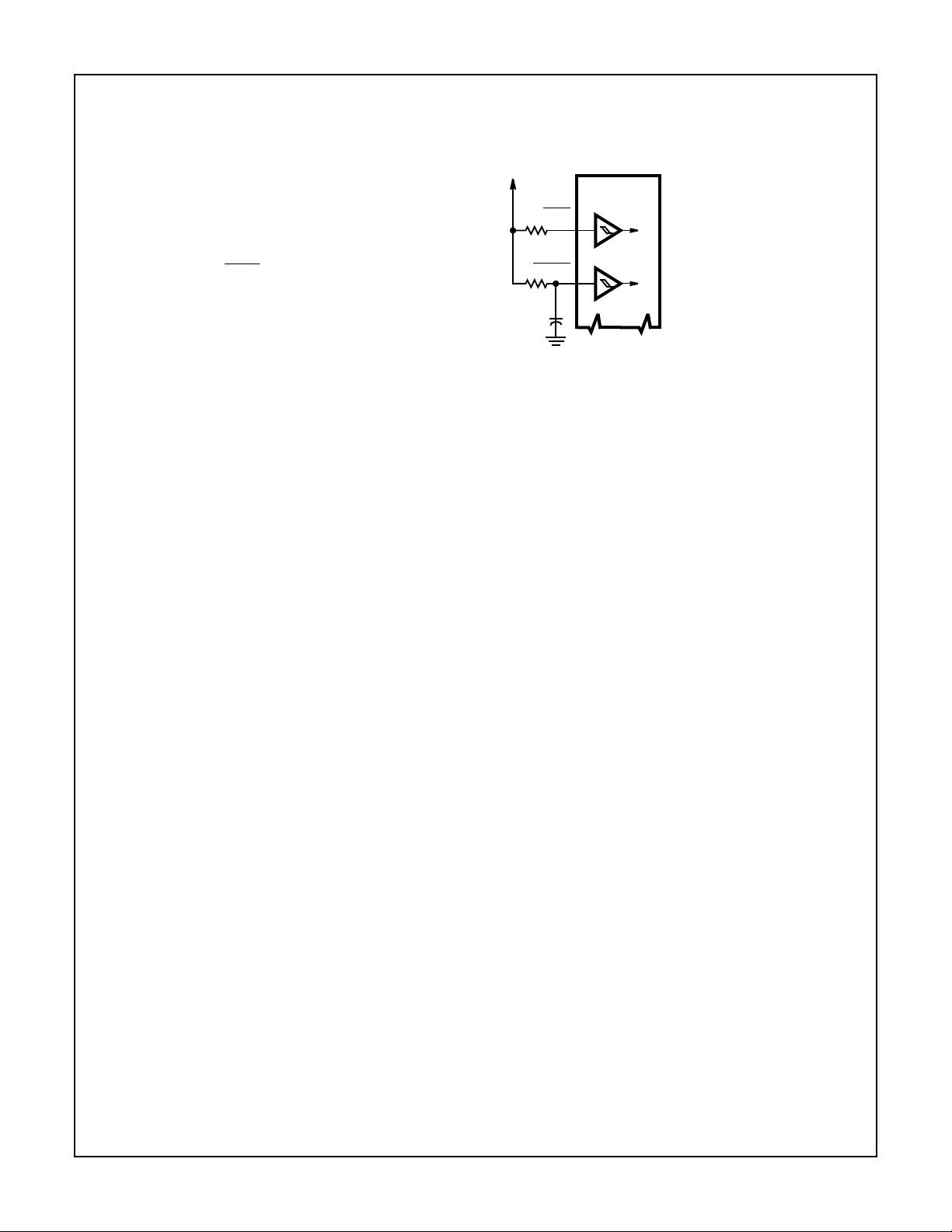
On-Board Clock (See Figure 8, Figure 9 and Figure 10)
Clock circuits may use either an external crystal or an RC
network.
A typical crystal oscillator circuit is shown in Figure 8. The
crystal is connected between terminals 1 and 39 (CLOCK
and XTAL
quency trimming capacitors, C
) in paral lel with a resistan ce, RF (1 mΩ typ). Fr e-
and C
IN
, may be required
OUT
at terminals 1 and 39. For additional information on crystal
oscillators, see lCAN-6565.
13

TPA
EF1
STPC
÷ 32
R
SCMI
SPMI
CDP1805AC, CDP1806AC
STM
INH
OUT
8-BIT
DOWN
COUNTER
LOAD
COUNTER
UNDERFLOW
ETQ
LDC
TO INTERRUPT LATCH
C
Q FF
DQ
Q OUTPUT
Q
READ
DTC
GEC
EF2
SPM2
SCM2
FIGURE 7. TIMER/COUNTER DIAGRAM
Because of the Schmitt Trigger input, an RC oscillator can
be used as shown in Figure 9. The frequency is approximately 1/RC (see Figure 10).
RF
1MΩ
CLOCK†
1 39 XTAL †
XTAL
5MHz PARALLEL
C
15pF
IN
RESONANT
CRYSTAL
C
OUT
27pF
VDD = 5V AT 25oC
10M
C
=
1M
R (Ω)
100K
10K
11M10 100 1K 10K 100K
C
=
1
C
=
0
.
1
µ
F
µ
p
F
FREQUENCY (Hz)
C
1
=
0
0
.
0
1
µ
F
C
=
1
0
0
p
F
0
0
p
F
†Pin numbers refer to 40 pin DIP.
FIGURE 8. TYPICAL 5MHz CRYSTAL OSCILLATOR
R
CLOCK†
†Pin numbers refer to 40 pin DIP.
1 39 XTAL †
C
FIGURE 9. RC NETWORK FOR OSCILLATOR
FIGURE 10. NOMINAL COMPONENT VALUES AS A FUNCTION
OF FREQUENCY FOR THE RC OSCILLATOR
CONTROL MODES
CLEAR
WAIT MODE
LL Not Allowed
L H Reset
H L Pause
HH Run
14
CDP1805AC, CDP1806AC
The function of the modes are defined as follows:
Reset
The levels on the CDP1805A and C DP1806A ex ternal si gnal
lines will asynchronously be forced by RESET to the following states:
Q = 0 SC1, SC0 = 0,1 BUS 0-7 = 0
MRD = 1 (EXECUTE) MA0-7 = RO.1
TPB = 0 N0, N1, N2 = 0, 0, 0 TPA = 0
Internal Changes Caused By RESET are:
l, N Instruction Register i s cl eared to 00. XlE and CIE are set
to allow interrupts following initialize. ClL is cleared (any
pending counter interrupt is cleared), counter is stopped, the
counter mode is cleared, and ETQ is disabled.
Initialization Cycle
The first machine cycle following termination of RESET is an
initialization cycle which requires 9 clock pulses. During this
cycle the CPU remains in S1 and the following additional
changes occur:
1 → MlE
→ T (The old value of X, P will be put into T. This
X, P
only has meaning following an orderly Reset with power
applied).
X, P, RO ← 0 (X, P, and RO are cleared).
Interrupt and DMA servicing is suppressed during the initialization cycle. The next cycle is an S0 or an S2 but never an
S1 or S3.The use of a 71 instruction followed by 00 at memory locations 0000 and 0001, may be used to reset MIE so
as to preclude interrupts until ready for them.
Reset and Initialize Do Not Affect:
D (Accumulator)
DF
R1, R2, R3, R4, R5, R6, R7, R8, R9, FA, RB, RC, RD, RE, RF
CH (Counter Holding Register)
Counter (the counter i s sto pped b ut the val ue is unaf fecte d)
MWR
= 1
Power-up Reset/Run Circuit
Power-up Reset/Run can be realized with the circuit shown
in Figure 11.
V
DD
R
R
CDP1805AC
CDP1806AC
WAIT
P
X
CLEAR
C
X
FIGURE 11. RESET/RUN DIAGRAM
THE RC TIME CONSTANT
SHOULD BE GREATER THAN
THE OSCILLATOR START-UP
TIME (TYPICALLY 20ms)
Pause
Pause is a low power mode which stops the internal CPU
timing generator and freezes the state of the processor. The
CPU may be held in the Pause mode indefinitely. Hardware
pause can occur at two points in a machine cycle, on the
low-to-high transition of either TPA or TPB. A TPB pause can
also be initiated by software with the execution of an IDLE
instruction. In the pa use mode , th e oscill ator c ontinue s to ru n
but subsequent clock transitions are ignored. TPA and TPB
remain at their previous state (see Figure 12).
Pause is entered from RUN by dropping WAIT low. Appropriate Setup and Hold times must be met.
If Pause is entered while in the event counter mode, the
appropriate Flag transition will continue to decrement the
counter.
Hardware-initiated pause is exited to RUN by raising the
Wait line high. Pause entered with an IDLE instruction
requires DMA, INTERRUPT or RESET to resume execution.
Run
May be initiated from the Pause or Reset mode functions. If
initiated from Pause, the CPU resumes operation at the
point it left off. If paused at TPA, it will resume on the next
high-to-low clock transition, while if paused at TPB, it will
resume on the next low-to-high clock transition (see Figure
12). When initiated from the Reset operation, the first
machine cycle following Reset is always the initialization
cycle. The i nit ia l iz ati o n cy cl e is the n f oll owed by a DMA (S2 )
cycle or fetch (S0) from location 0000 in memory.
Schmitt Trigger Inputs
All inputs except BUS 0-BUS 7 and ME contain a Schmitt
Trigger c irc uit , which is especially u se ful on the CLEAR input
as a power-up RESET (see Figure 11) and the CLOCK input
(see Figure 8 and Figure 9).
15

State Transitions
CDP1805AC, CDP1806AC
The CDP1805A and CDP1806A state transitions are shown
in Figure 13 . Each mach ine cycle requires t he same pe riod
of time, 8 clock pu lses, except the ini tialization cyc le (INlT)
ENTER
RESUME
CLOCK
TPA
WAIT
PAUSE
70 71 00 01 10 11 20 21
t
PLH
tSUt
FIGURE 12A. TPA PAUSE TIMING
PAUSE
PAUSE
H
RUN
30
t
PHL
t
SU
FIGURE 12. P AUSE MODE TIMING WAVEFORMS
RESET
PAUSE
which requi res 9 clock pulses. Re set is asynchronous a nd
can be forced at any time.
ENTER
RESUME
PAUSE
CLOCK
TPB
WAIT
50 51 60 61 70 71 00 01 10
t
PLH
tSUt
NOTE:
9. Pause (in clock waveform) while represented here as one clock
cycle in duration, could be infinitely long.
FIGURE 12B. TPB PAUSE TIMING
• DMA • RESET
INT
PAUSE
H
RUN
PAUSE
t
PHL
t
SU
S1 RESET
S1 INIT
DMA DMA
S2 DMA
IDLE • DMA • INT
DMA + INT
DMA • FORCE
DMA • INT
S1
S1 EXECUTE
DMA
SO FETCH
“68”
DMA
INT • DMA
FORCE S1
(LONG BRANCH,
LONG SKIP, NOP, RSXD, ETC)
DMA
• FORCE S1
FORCE S0
FIGURE 13. STATE TRANSITION DIAGRAM
• IDLE • INT
FORCE S0
DMA
S3 INT
INT • DMA
PRIORITY: RESET
• FORCE S1
FORCE S0, S1
DMA
IN
DMA
OUT
INT
16

Instruction Set
CDP1805AC, CDP1806AC
The CDP1805AC and CDP1806AC instruction summary is
given in Table 1. Hexadecimal notation is used to refer to the
4-bit binary codes.
In all registers, bits are numbered from the least significant
bit (LSB) to the most significant bit (MSB) starting with 0.
R(W): Register designated by W, where
W = N or X, or P
TABLE 1. INSTRUCTION SUMMARY (SEE NOTES)
NO. OF
INSTRUCTION
MEMORY REFERENCE
LOAD IMMEDIATE 2 LDI F8 M(R(P)) → D; R(P) + 1 → R(P)
REGISTER LOAD IMMEDIATE 5 RLDI 68CN
LOAD VIA N 2 LDN 0N M(R(N)) → D; FOR N NOT 0
LOAD ADVANCE 2 LDA 4N M(R(N)) → D; R(N) + 1 → R(N)
LOAD VIA X 2 LDX F0 M(R(X)) → D
LOAD VIA X AND ADVANCE 2 LDXA 72 M(R(X )) → D; R(X) + 1 → R(X)
REGISTER LOAD VIA X AND
ADVANCE
STORE VIA N 2 STR 5N D → M(RN))
STORE VIA X AND DECREMENT 2 STXD 73 D → M(R(X)); R(X) - 1 → R(X)
REGISTER STOR E VIA X AND
DECREMENT
REGISTER OPERATIONS
INCREMENT REG N 2 INC 1N R(N) + 1 → R(N)
DECREMENT REG N 2 DEC 2N R(N) - 1 → R(N)
DECREMENT REG N AND LONG
BRANCH IF NOT EQUAL 0
INCREMENT REG X 2 IRX 60 R(X) + 1 → R(X)
GET LOW REG N 2 GLO 8N R(N).0 → D
PUT LOW REG N 2 PLO AN D → R(N).0
GET HIGH REG N 2 GHI 9N R(N).1 → D
PUT HIGH REG N 2 P HI BN D → R(N).1
REGISTER N TO REGISTER X
COPY
LOGIC OPERATIONS (Note 19)
OR 2 OR F1 M(R(X)) OR D → D
OR IMMEDIATE 2 ORI F9 M(R(P)) OR D → D; R(P) + 1 → R(P)
EXCLUSIVE OR 2 XOR F3 M(R(X)) XOR D → D
EXCLUSIVE OR IMMEDIATE 2 XRI FB M(R(P)) XOR D → D;
AND 2 AND F2 M(R(X)) AND D → D
MACHINE
CYCLES MNEMONIC OP CODE OPERATION
5 RLXA 686N
5 RSXD 68AN
5 DBNZ 682N R(N) - 1 → R(N); IF R(N) NOT 0,
4 RNX 68BN
R(W).0: Lower-order byte of R(W)
R(W).1: Higher-order byte of R(W)
Operation Notation
M (R(N)) → D; R(N) + 1 → R(N)
This notation means: The memory byte pointed to by R(N) is
loaded into D, and R(N) is incremented by 1.
M(R(P)) → R(N).1; M(R(P)) + 1 →
(Note 10)
(Note 10)
(Note 10)
(Note 10)
R(N).0; R(P) + 2 → R(P)
M(R(X)) → R(N).1; M(R(X) + 1) →
R(N).0; R(X)) + 2 → R(X)
R(N).0 → M(R(X)); R(N).1 →
M(R)(X) - 1); R(X) - 2 → R (X)
M(R(P)) → R(P).1, M(R(P) + 1) →
R(P).0, ELSE R(P) + 2 → R(P)
R(N) → R(X)
R(P) + 1 → R(P)
17

CDP1805AC, CDP1806AC
TABLE 1. INSTRUCTION SUMMARY (SEE NOTES) (Continued)
NO. OF
INSTRUCTION
AND IMMEDIATE 2 ANI FA M(R(P)) AND D → D; R(P) + 1 → R(P)
SHIFT RIGHT 2 SHR F6 Shift D Right, LSB(D) → DF, 0 → MSB(D)
SHIFT RIGHT WITH CARRY 2 SHRC 76
RING SHIFT RIGHT 2 RSHR 76
SHIFT LEFT 2 SHL FE SHIFT D LEFT, MSB(D) → DF, 0 → LSB(D)
SHIFT LEFT WITH CARRY 2 SHLC 7E
RING SHIFT LEFT 2 RSHL 7E
ARITHMETIC OPERATIONS (Note 3)
ADD 2 ADD F4 M(R(X)) + D → DF, D
DECIMAL ADD 4 DADD 68F4 M(R(X)) + D → DF, D DECIMAL ADJUST → DF, D
ADD IMMEDIATE 2 ADI FC M (R(P )) + D → DF, D; R(P) + 1 → R(P)
DECIMAL ADD IMMEDIATE 4 DADI 68FC M(R(P)) + D → DF, D; R(P) + 1 → R(P)
ADD WITH CARRY 2 ADC 74 M (R(X)) + D + DF → DF, D
DECIMAL ADD WITH CARRY 4 DADC 6874 M(R(X)) + D + DF → DF, D
ADD WITH CARRY, IMMEDIATE 2 ADCI 7C M(R(P)) + D + DF → DF, D;
DECIMAL ADD WITH CARRY,
IMMEDIATE
SUBTRACT D 2 SD F5 M(R(X)) - D → DF, D
SUBTRACT D IMMEDIATE 2 SDI FD M(R(P)) - D → DF, D;
SUBTRACT D WITH BORROW 2 SDB 75 M(R(X)) - D - (NOT DF) → DF, D
SUBTRACT D WITH BORROW,
IMMEDIATE
SUBTRACT MEMORY 2 SM F7 D - M(R(X)) → DF, D
DECIMAL SUBTRACT MEMORY 4 DSM 68F7 D - M(R(X)) → DF, D; DECIMAL ADJUST → DF, D
SUBTRACT MEMORY IMMEDIAT E 2 SMI FF D - M(R(P)) → DF, D; R(P) + 1 → R(P)
DECIMAL SUBTRACT MEMORY,
IMMEDIATE
SUBTRACT MEMORY WITH
BORROW
DECIMAL SUBTRACT MEMORY
WITH BORROW
SUBTRACT MEMORY WITH
BORROW, IMMEDIATE
MACHINE
CYCLES MNEMONIC OP CODE OPERATION
Shift D Right, LSB(D) → DF, DF → MSB(D)
(Note 11)
SHIFT D RIGHT, LSB(D) → DF, DF → MSB(D)
(Note 11)
SHIFT D LEFT, MSB(D) → DF, DF → LSB(D)
(Note 11)
SHIFT D LEFT, MSB(D) → DF, DF → LSB(D)
(Note 11)
DECIMAL ADJUST → DF, D
DECIMAL ADJUST → DF, D
R(P) + 1 → R(P)
4 DACI 687C M(R(P)) + D + DF → DF, D;
R(P) + 1 → R(P),
DECIMAL ADJUST → DF, D
R(P) + 1 → R(P)
2 SDBI 7D M(R(P)) - D - (NOT DF) → DF, D;
R(P) + 1 → R(P)
4 DSMI 68FF D - M(R(P)) → DF, D;
R(P) + 1 → R(P),
DECIMAL ADJUST → DF, D
2 SMB 77 D - M(R(X)) - (NOT DF) → DF, D
4 DSMB 6877 D - M(R( X)) - (NO T DF) → DF, D;
DECIMAL ADJUST → DF, D
2 SMBI 7F D - M(R(P)) - (NOT DF) → DF, D;
R(P) + 1 → R(P)
18

CDP1805AC, CDP1806AC
TABLE 1. INSTRUCTION SUMMARY (SEE NOTES) (Continued)
NO. OF
INSTRUCTION
DECIMAL SUBTRACT MEMORY
WITH BORROW, IMMEDIATE
BRANCH INSTRUCTIONS - SHORT BRANCH
SHORT BRANCH 2 BR 30 M (R(P )) → R(P).0
NO SHORT BRANCH (See SK P) 2 NBR 38
SHORT BRANCH IF D = 0 2 BZ 32 IF D = 0, M(R(P)) → R(P).0
SHORT BRANCH IF D NOT 0 2 BNZ 3A IF D NOT 0, M(R(P)) → R(P).0
SHORT BRANCH IF DF = 1 2 BDF 33
SHORT BRANCH IF POS OR ZERO 2 BPZ 33
SHORT BRANCH IF EQUAL OR
GREATER
SHORT BRANCH IF DF = 0 2 BNF 3B
SHORT BRANCH IF MINUS 2 BM 3B
SHORT BRANCH IF LESS 2 BL 3B
SHORT BRANCH IF Q = 1 2 BQ 31 IF Q = 1, M(R(P)) → R(P).0
SHORT BRANCH IF Q = 0 2 BNQ 39 IF Q = 0, M(R(P)) → R(P).0
SHORT BRANCH IF EF1 = 1
= VSS)
(EF1
SHORT BRANCH IF EF1 = 0
= VDD)
(EF1
SHORT BRANCH IF EF2 = 1
(EF2
= VSS)
SHORT BRANCH IF EF2 = 0
= VDD)
(EF2
SHORT BRANCH IF EF3 = 1
= VSS)
(EF3
SHORT BRANCH IF EF3 = 0
= VDD)
(EF3
SHORT BRANCH IF EF4 = 1
= VSS)
(EF4
SHORT BRANCH IF EF4 = 0
= VDD)
(EF4
SHORT BRANCH ON COUNTER
INTERRUPT
SHORT BRANCH ON EXTERNAL
INTERRUPT
MACHINE
CYCLES MNEMONIC OP CODE OPERATION
4 DSBI 687F D - M(R(P)) - (NOT DF) → DF, D
(Note 11)
(Note 11)
(Note 11)
2BGE33
(Note 11)
(Note 11)
(Note 11)
(Note 11)
2 B1 34 IF EF1 = 1, M(R(P)) → R(P).0
2 BN1 3C I F EF1 = 0, M(R(P)) → R(P).0
2 B2 35 IF EF2 = 1, M(R(P)) → R(P).0
2 BN2 3D I F EF2 = 0, M(R(P)) → R(P).0
2 B3 36 IF EF3 = 1, M(R(P)) → R(P).0
2 BN3 3E IF EF3 = 0, M(R(P)) → R(P).0
2 B4 37 IF EF4 = 1, M(R(P)) → R(P).0
2 BN4 3F IF EF4 = 0, M(R(P)) → R(P).0
3 BCI 683E
(Note 12)
3 BXI 683F IF XI = 1, M(R(P)) → R(P).0
R(P) + 1 → R(P)
DECIMAL ADJUST → DF, D
R(P) + 1 → R(P)
ELSE R(P) + 1 → R(P)
ELSE R(P) + 1 → R(P)
IF DF = 1, M(R(P)) → R(P).0
ELSE R(P) + 1 → R(P)
IF DF = 1, M(R(P)) → R(P).0
ELSE R(P) + 1 → R(P)
IF DF = 1, M(R(P)) → R(P).0,
ELSE R(P) + 1 → R(P)
IF D = 0, M(R(P)) → R(P).0,
ELSE R(P) + 1 → R(P)
IF D = 0, M(R(P)) → R(P).0,
ELSE R(P) + 1 → R(P)
IF D = 0, M(R(P)) → R(P).0,
ELSE R(P) + 1 → R(P)
ELSE R(P) + 1 → R(P)
ELSE R(P) + 1 → R(P)
ELSE R(P) + 1 → R(P)
ELSE R(P) + 1 → R(P)
ELSE R(P) + 1 → R(P)
ELSE R(P) + 1 → R(P)
ELSE R(P) + 1 → R(P)
ELSE R(P) + 1 → R(P)
ELSE R(P) + 1 → R(P)
ELSE R(P) + 1 → R(P)
IF CI = 1, M(R(P)) → R(P).0; 0 → CI
ELSE R(P) + 1 → R(P)
ELSE R(P) + 1 → R(P)
19

CDP1805AC, CDP1806AC
TABLE 1. INSTRUCTION SUMMARY (SEE NOTES) (Continued)
NO. OF
INSTRUCTION
BRANCH INSTRUCTIONS - LONG BRANCH
LONG BRANCH 3 LBR C0 M(R(P)) → R(P).1, M(R(P) + 1) → R(P).0
NO LONG BRANCH (See LSKP) 3 NLBR C8
LONG BRANCH IF D = 0 3 LBZ C2 IF D = 0, M(R(P)) → R(P).1
LONG BRANCH IF D NOT 0 3 LBNZ CA IF D NOT 0, M(R(P)) → R(P).1
LONG BRANCH IF DF = 1 3 LBDF C3 IF DF = 1, M(R(P)) → R(P).1
LONG BRANCH IF DF = 0 3 LBNF CB IF DF = 0, M(R(P)) → R(P).1
LONG BRANCH IF Q = 1 3 LBQ C1 IF Q = 1, M(R(P)) → R(P).1
LONG BRANCH IF Q = 0 3 LBNQ C9 IF Q = 0, M(R(P)) → R(P).1
SKIP INSTRUCTIONS
SHORT SKIP (See NBR) 2 SKP 38
LONG SKIP (See NLBR) 3 LSKP C8
LONG SKIP IF D = 0 3 LSZ CE IF D = 0, R(P) + 2 → R(P)
LONG SKIP IF D NOT 0 3 LSNZ C6 IF D NOT 0, R(P) + 2 → R(P)
LONG SKIP IF DF = 1 3 LSDF CF IF DF = 1, R(P) + 2 → R(P)
LONG SKIP IF DF = 0 3 LSNF C7 IF DF = 0, R(P) + 2 → R(P)
LONG SKIP IF Q = 1 3 LSQ CD IF Q = 1, R(P) + 2 → R(P)
LONG SKIP IF Q = 0 3 LSNQ C5 IF Q = 0, R(P) + 2 → R(P)
LONG SKIP IF MIE = 1 3 LSIE CC IF MIE = 1, R(P) + 2 → R(P)
CONTROL INSTRUCTIONS
IDLE 2 IDL 00
NO OPERATIO N 3 NOP C4 CONTINUE
SET P 2 SEP DN N → P
SET X 2 SEX EN N → X
MACHINE
CYCLES MNEMONIC OP CODE OPERATION
R(P) + 2 → R(P)
(Note 11)
M(R(P) + 1) → R(P).0
ELSE R(P) + 2 → R(P)
M(R(P) + 1) → R(P).0
ELSE R(P) + 2 → R(P)
M(R(P) + 1) → R(P).0
ELSE R(P) + 2 → R(P)
M(R(P) + 1) → R(P).0
ELSE R(P) + 2 → R(P)
M(R(P) + 1) → R(P).0
ELSE R(P) + 2 → R(P)
M(R(P) + 1) → R(P).0
ELSE R(P) + 2 → R(P)
R(P) + 1 → R(P)
(Note 11)
(Note 11)
(Note 14)
R(P) + 2 → R(P)
ELSE CONTINUE
ELSE CONTINUE
ELSE CONTINUE
ELSE CONTINUE
ELSE CONTINUE
ELSE CONTINUE
ELSE CONTINUE
STOP ON TPB; WAIT FOR DMA OR INTERRUPT;
BUS FLOATS
20

CDP1805AC, CDP1806AC
TABLE 1. INSTRUCTION SUMMARY (SEE NOTES) (Continued)
NO. OF
INSTRUCTION
SET Q 2 SEQ 7B 1 → Q
RESET Q 2 REQ 7A 0 → Q
PUSH X, P TO STACK 2 MARK 79 (X, P) → T; (X, P) → M(R(2)),
TIMER/COUNTER INSTRUCTIONS
LOAD COUNTER 3 LDC 6806
GET COUNTER 3 GEC 6808 CNTR → D
STOP COUNTER 3 STPC 6800 STOP CNTR CLOCK;
DECREMENT TIMER/COUNTER 3 DTC 6801 CNTR - 1 → CNTR
SET TIMER MODE AND START 3 STM 6807 TPA ÷ 32 → CNTR
SET COUNTER MODE 1 AND
START
SET COUNTER MODE 2 AND
START
SET PULSE WIDTH MODE 1 AND
START
SET PULSE WIDTH MODE 2 AND
START
ENABLE TOGGLE Q 3 E TQ 6809
INTERRUPT CONTROL
EXTERNAL INTERRUPT ENABLE 3 XIE 680A 1 → XIE
EXTERNAL INTERRUPT DISABLE 3 XID 680B 0 → XIE
COUNTER INTERRUPT ENABLE 3 CIE 680C l → CIE
COUNTER INTERRUPT DISABLE 3 CID 680D 0 → CIE
RETURN 2 RET 70 M(R(X)) → X, P; R(X) + 1 → R(X); 1 → MIE
DISABLE 2 DIS 7 1 M(R(X) → X, P; R(X) + 1 → R(X); 0 → MIE
SAVE 2 SAV 78 T → M(R(X))
SAVE T, D, DF 6 DSAV 6876
INPUT-OUTPUT BYTE TRANSFER
OUTPUT 1 2 OUT 1 61 M(R(X)) → BUS; R(X) + 1 → R(X)
OUTPUT 2 2 OUT 2 62 M(R(X)) → BUS; R(X) + 1 → R(X)
OUTPUT 3 2 OUT 3 63 M(R(X)) → BUS; R(X) + 1 → R(X)
OUTPUT 4 2 OUT 4 64 M(R(X)) → BUS; R(X) + 1 → R(X)
OUTPUT 5 2 OUT 5 65 M(R(X)) → BUS; R(X) + 1 → R(X)
MACHINE
CYCLES MNEMONIC OP CODE OPERATION
THEN P → X; R(2) → 1→ R(2)
CNTR STOPPED: D → CH, CNTR;
(Note 15)
3 SCM1 6805 EF1
3 SCM2 6803 EF2
3 SPM1 6804 TPA.EF1
3 SPM2 6802 TPA.EF2 → CNTR CLOCK;
(Note 15)
(Note 10)
0 → CI. CNTR RUNNING; D → CH
0 → ÷ 32 PRESCALER
→ CNTR CLOCK
→ CNTR CLOCK
→ CNTR CLOCK;
EF1
EF2
IF CNTR = 01 • NEXT CNTR CLOCK ; Q
R(X) - 1 → R(X), T → M(R(X)),
R(X) - 1 → R(X), D → M (R(X)) ,
R(X) - 1 → R(X), SHIFT D
RIGHT WITH CARRY, D → M(R(X))
N LINES = 1
N LINES = 2
N LINES = 3
N LINES = 4
N LINES = 5
STOPS COUNT
STOPS COUNT
→ Q
21

CDP1805AC, CDP1806AC
TABLE 1. INSTRUCTION SUMMARY (SEE NOTES) (Continued)
NO. OF
INSTRUCTION
OUTPUT 6 2 OUT 6 66 M(R(X)) → BUS; R(X) + 1 → R(X)
OUTPUT 7 2 OUT 7 67 M(R(X)) → BUS; R(X) + 1 → R(X)
INPUT 1 2 INP 1 69 BUS → M(R(X )); BUS → D
INPUT 2 2 INP 2 6A BUS → M(R (X )); BUS → D
INPUT 3 2 INP 3 6B BUS → M(R (X )); BUS → D
INPUT 4 2 INP 4 6C BUS → M(R(X)); BUS → D
INPUT 5 2 INP 5 6D BUS → M(R(X)); BUS → D
INPUT 6 2 INP 6 6E BUS → M(R (X )); BUS → D
INPUT 7 2 INP 7 6F BUS → M(R(X)); BUS → D
CALL AND RETURN
STANDARD CALL 10 SCAL 688N
STANDARD RETURN 8 SRET 689N
MACHINE
CYCLES MNEMONIC OP CODE OPERATION
N LINES = 6
N LINES = 7
N LINES = 1
N LINES = 2
N LINES = 3
N LINES = 4
N LINES = 5
N LINES = 6
N LINES = 7
(Note 10)
(Note 10)
R(N).0 → M(R(X));
R(N).1 → M(R(X) - 1);
R(X) - 2 → R(X); R(P) → R(N);
THEN M(R(N)) → R(P).1;
M(R(N) + 1) → R(P).0;
R(N) + 2 → R(N)
R(N) → R(P);
M(R(X) + 1) → R(N).1;
M(R(X) + 2) → R(N).0; R(X) + 2 → R(X)
NOTES:
10. Previous contents of T register are destroyed during instruction execution.
11. This instruction is associated with more than one mnemonic. Each mnemonic is individually listed.
12. ETQ cleared by LDC with the Counter/Timer stopped, reset of CPU, or BCl • (Cl = 1).
13. Cl = Counter Interrupt, Xl = External Interrupt.
14. An IDLE instruction initiates an S1 cycle. All external signals, except the oscillator, are stopped on the low-to-high transition of TPB. All
outputs remain in their previous states, MRD
until an I/O request (INTERRUPT, DMA-IN, or DMA-OUT) is activated. When the request is acknowledged, the IDLE cycle is terminated
and the I/O request is serviced, and the normal operation is resumed. (To respond to an lNTERRUPT during an IDLE, MlE and either
ClE or XlE must be enabled).
15. Long-Branch, Long-Skip and No Op instructions require three cycles to complete (1 fetch + 2 execute).
Long-Branch instructions are three bytes long. The first byte specifies the condition to be te sted; and the second and third byte, the
branching address.
The long branch instruction can:
a. Branch unconditionally
b. Test for D = 0 or D ≠ 0
c. Test for DF = 0 or DF = 1
d. Test for Q = 0 or Q = 1
e. Effect an unconditional no branch
If the tested condition is met, then branching takes place; the branching address bytes are loaded in the high-and-low-order bytes of the
current program counter, respectively. This operation effects a branch to any memory location.
If the tested condition is not met, the branching address bytes are skipped over, and the next instruction in sequence is fetched and executed. This operation is taken for the case of unconditional no branch (NLBR).
, MWR, are set to a logic ‘1’ and the data bus floats. The processor will continue to IDLE
22

CDP1805AC, CDP1806AC
16. The short-branch instructions are two or three bytes long. The first byte specifies the condition to be tested, and the second specifies the
branching address, except for the branches on interrupt. For those, the first two bytes specify the condition to be tested and the third byte
specifies the branching address.
The short branch instruction can:
a. Branch unconditionally
b. Test for D = 0 or D ≠ 0
c. Test for DF = 0 or DF = 1
d. Test for Q = 0 or Q = 1
e. Test the status (1 or 0) of the four EF flags
f. Effect an unconditional no branch
g. Test for counter or external interrupts (BCI, BXI)
If the tested condition is met, then branching takes place; the branching address byte is loaded into the low-order byte position of the
current program counter. This effects a branch within the current 256-byte page of the memory, i.e., the page which holds the branching
address. If the tested condition is not met, the branching address byte is skipped over, and the next instruction in sequence is fetched
and executed. This same action is taken in the case of unconditional no branch (NBR).
17. The skip instructions are one byte long. There is one Unconditional Short-Skip (SKP) and eight Long-Skip instructions.
The Unconditional Short-Skip instruction takes 2 cycles to complete (1 fetch + 1 execute). Its action is to skip over the byte following it.
Then the next instruction in sequence is fetched and executed. This SKP instruction is identical to the unconditional No-Branch Instruction (NBR) except that the skipped-over byte is not considered part of the program.
The Long-Skip instructions take three cycles to complete (1 fetch + 2 execute).
They can:
a. Skip unconditionally
b. Test for D = 0 or D ≠ 0
c. Test for DF = 0 or DF = 1
d. Test for Q = 0 or Q = 1
e. Test for MIE = 1
If the tested condition is met, then Long Skip takes place; the current program counter is incremented twice. T hus, two bytes are
skipped over and the next instruction in sequence is fet ched and executed. If the tested condition is not met, then no action is taken.
Execution is continued by fetching the next instruction in sequence.
18. Instruction 6800 through 68FF take a minimum of 3 machine cycles and up to a maximum of 10 machine cycles. In all cases, the first two
cycles are fetches and subsequent cycles are execut es. The firs t byte (68) of the se two-byte op codes is used to genera te the second
fetch, the second byte is then interpreted differently than the same code without the 68 prefix. DMA and INT requests are not serviced
until the end of the last execute cycle.
19. Arithmetic Operations:
The arithmetic and shift operations are the only instructions that can alter the content of DF. The syntax ‘(NOT DF)’ denotes the subtrac-
tion of the borrow.
Binary Operations:
After an ADD instruction
DF = 1 denotes a carry has occurred. Result is greater than FF
DF = 0 denotes a carry has not occurred.
After a SUBTRACT instruction
DF = 1 denotes no borrow. D is a true positive number.
DF = 0 denotes a borrow. D is in two's complement form.
Binary Coded Decimal Operations:
After a BCD ADD instruction
DF = 1 denotes a carry has occurred. Result is greater than 99
DF = 0 denotes a carry has not occurred.
After a BCD SUBTRACT instruction
DF = 1 denotes no borrow. D is a true positive decimal number.
Example 9 9 D
-88
11 D DF = 1
DF = 0 denotes a borrow. D is in ten's complement form.
Example 8 8 D
-99
89 D DF = 0
89 is the ten's complement of 11, which is the correct answer (with a minus value denoted by DF = 0).
M(R(X))
M(R(X))
.
16
.
10
23

CDP1805AC, CDP1806AC
TABLE 2. CONDITIONS ON DATA BUS AND MEMORY ADDRESS LINES DURING ALL MACHINE STATES
DATA
STATE I N MNEMONIC OPERATION
S1 RESET 0 → Q, I, N, COUNTER,
PRESCALER, CIL;
1 → CIE, XIE
S1 INITIALIZE, NOT PROGRAMMER AC-
CESSIBLE
S0 FETCH MRP → I, N; RP + 1 → RP MRP RP 0 1 0
S1 0 0 IDL STOP AT TPB
S1 0 1-F LDN MRN → D MRN RN 0 1 0
S1 1 0-F INC RN + 1 → RN HIGH Z RN 1 1 0
S1 2 0-F DEC RN - 1 → RN HIGH Z RN 1 1 0
S1 3 0-F SHORT
BRANCH
S1 4 0-F LDA MRN → D; RN + 1 → RN MRN RN 0 1 0
S1 5 0-F STR D → MRN D RN 1 0 0
S1 6 0 IRX RX + 1 → RX MRX RX 1 1 0
S1 6 1 OUT 1 MRX → BUS; RX + 1 → RX MRX RX 0 1 1
S1 6 2 OUT 2 MRX → BUS; RX + 1 → RX MRX RX 0 1 2
X, P → T THEN
0 → X, P; 1 → MIE, 0000 → R000(Note 20)
WAIT FOR DMA OR INT
TAKEN: MRP → RP.0
NOT TAKEN: RP + 1 → RP
BUS
00 UNDE-
HIGH Z RO 1 1 0
MRP RP 0 1 0
MEMORY
ADDRESS MRD
11 0
FINED
UNDE-
FINED
110
MWR
N
LINES
S1 6 3 OUT 3 MRX → BUS; RX + 1 → RX MRX RX 0 1 3
S1 6 4 OUT 4 MRX → BUS; RX + 1 → RX MRX RX 0 1 4
S1 6 5 OUT 5 MRX → BUS; RX + 1 → RX MRX RX 0 1 5
S1 6 6 OUT 6 MRX → BUS; RX + 1 → RX MRX RX 0 1 6
S1 6 7 OUT 7 MRX → BUS; RX + 1 → RX MRX RX 0 1 7
S1 6 9 INP 1 BUS → MRX, D DATA
FROM
I/O
DEVICE
S1 6 A IN P 2 BUS → MRX, D DATA
FROM
I/O
DEVICE
S1 6 B INP 3 BUS → MRX, D DATA
FROM
I/O
DEVICE
S1 6 C INP 4 BUS → MRX, D DATA
FROM
I/O
DEVICE
S1 6 D INP 5 BUS → MRX, D DATA
FROM
I/O
DEVICE
RX 1 0 1
RX 1 0 2
RX 1 0 3
RX 1 0 4
RX 1 0 5
24

CDP1805AC, CDP1806AC
TABLE 2. CONDITIONS ON DATA BUS AND MEMORY ADDRESS LINES DURING ALL MACHINE STATES (Continued)
STATE I N MNEMONIC OPERATION
S1 6 E INP 6 BUS → MRX, D DATA
S1 6 F INP 7 BUS → MRX, D DATA
S1 7 0 RET MRX → X, P; RX + 1 → RX
1 → MIE
S1 7 1 DIS MRX → X, P; RX + 1 → RX
0 → MIE
S1 7 2 LDXA MRX → D; RX + 1 → RX MRX RX 0 1 0
S1 7 3 STXD D → MRX; RX - 1 → RX D RX 1 0 0
S1 7 4 ADC MRX + D + DF → DF, D MRX RX 0 1 0
S1 7 5 SDB MRX - D - DFN → DF, D MRX RX 0 1 0
S1 7 6 SHRC LSB(D) → DF; DF → MSB(D) HIGH Z RX 1 1 0
S1 7 7 SMB D - MRX - DFN → DF, D MRX RX 0 1 0
S1 7 8 SAV T → MRX T RX 1 0 0
DATA
BUS
FROM
I/O
DEVICE
FROM
I/O
DEVICE
MRX RX 0 1 0
MRX RX 0 1 0
MEMORY
ADDRESS MRD
RX 1 0 6
RX 1 0 7
MWR
N
LINES
S1 7 9 MARK X, P → T, MR2; P → X
S1 7 A REQ 0 → QHIGH ZRP110
S1 7 B SEQ 1 → QHIGH ZRP110
S1 7 C ADCI MRP + D + DF → DF, D; RP + 1 MRP RP 0 1 0
S1 7 D SDBI MRP - D - DFN → DF, D; RP + 1 MRP RP 0 1 0
S1 7 E SHLC MSB(D) → DF; DF → LSB D HIGH Z RP 1 1 0
S1 7 F SMBI D - MRP - DFN → DF, D; RP + 1 MRP RP 0 1 0
S1 8 0-F GLO RN.0 → D RN.0 RN 1 1 0
S1 9 0-F GHI RN.1 → D RN.1 RN 1 1 0
S1 A 0-F PLO D → RN.0 D RN 1 1 0
S1 B 0-F PHI D → RN.1 D RN 1 1 0
S1#1 C 0-3,
8-B
#2 C 0-3,
8-B
S1#1 C 0-3,
8-B
#2 C 0-3,
8-B
LONG
BRANCH
LONG
BRANCH
LONG
BRANCH
LONG
BRANCH
R2 - 1 → R2
TAKEN: MRP → B; RP + 1 → RP MRP RP 0 1 0
TAKEN: B → RP.1; MRP →
RP.0
NOT TAKEN RP + 1 → RP MRP RP 0 1 0
NOT TAKEN RP + 1 → RP M(RP + 1) RP + 1 0 1 0
T R2 1 0 0
M(RP + 1) RP + 1 0 1 0
S1#1 C 5 LONG
SKIP
#2 C 6 LONG
SKIP
TAKEN: RP + 1 → RP MRP RP 0 1 0
TAKEN: RP + 1 → RP M(RP + 1) RP + 1 0 1 0
25

CDP1805AC, CDP1806AC
TABLE 2. CONDITIONS ON DATA BUS AND MEMORY ADDRESS LINES DURING ALL MACHINE STATES (Continued)
STATE I N MNEMONIC OPERATION
#2 C 7 LONG
SKIP
S1#1 C C LONG
SKIP
S1#1 C D LONG
SKIP
#2 C E LONG
SKIP
S1#1 C F LONG
SKIP
S1#1 C 4 NOP NO OPERATION MRP RP 0 1 0
#2 C 4 NOP NO OPERATION M(RP + 1) RP + 1 0 1 0
S1 D 0-F SEP N → PNNRN110
S1 E 0-F SEX N → XNNRN110
S1 F 0 LDX MRX → D MRX RX 0 1 0
S1 F 1 OR MRX OR D → D MRX RX 0 1 0
S1 F 2 AND MRX AND D → D MRX RX 0 1 0
S1 F 3 XOR MRX XOR D → D MRX RX 0 1 0
TAKEN: RP + 1 → RP M(RP + 1) RP + 1 0 1 0
NOT TAKEN: NO OPERATION MRP RP 0 1 0
NOT TAKEN: NO OPERATION MRP RP 0 1 0
NOT TAKEN: NO OPERATION M(RP + 1) RP + 1 0 1 0
NOT TAKEN: NO OPERATION M(RP + 1) RP + 1 0 1 0
DATA
BUS
MEMORY
ADDRESS MRD
MWR
N
LINES
S1 F 4 ADD MRX + D → DF, D MRX RX 0 1 0
S1 F 5 SD MRX - D → DF, D MRX RX 0 1 0
S1 F 7 SM D - MRX → DF; D MRX RX 0 1 0
S1 F 6 SHR LSB(D) → DF; 0 → MSB(D) HIGH Z RX 1 1 0
S1 F 8 LDI MRP → D; RP + 1 → RP MRP RP 0 1 0
S1 F 9 ORI MRP OR D → D; RP + 1 → RP MRP RP 0 1 0
S1 F A ANI MRP AND D → D; RP + 1 → RP MRP RP 0 1 0
S1 F B XRI MRP XOR D → D; RP + 1 → RP MRP RP 0 1 0
S1 F C ADI MRP + D → DF, D; RP + 1 → RP MRP RP 0 1 0
S1 F D SDI MRP - D → DF, D; RP + 1 → RP MRP RP 0 1 0
S1 F F SMI D - MRP → DF, D; RP + 1 → RP MRP RP 0 1 0
S1 F E SHL MSB(D) → DF; 0 → LSB(D) HIGH Z RP 1 1 0
S2 DMA IN DMA IN DMA IN BUS → MR0; R0 + 1 → R0 DATA
S2 DMA OUT DMA
S3 INTER-
RUPT
OUT
INTER-
RUPT
DMA OUT MRO → BUS; R0 + 1 → R0 MR0 R0 0 1 0
INTERRUPT X, P → T; 0 → MIE
1 → P; 2 → X
FROM I/O
DEVICE
HIGH Z RN 1 1 0
R0 1 0 0
THE FOLLOWING ARE ALL LINKED INSTRUCTIONS “68” PRECEEDS ALL OP CODES, SO THERE IS A DUPLICATE FETCH
S1 0 0 STPC STOP COUNTER CLOCK;
0 → ÷ 32 PRESCALER
S1 0 1 DTC CNTR - 1 → CNTR HIGH Z R1 1 1 0
HIGH Z R0 1 1 0
26

CDP1805AC, CDP1806AC
TABLE 2. CONDITIONS ON DATA BUS AND MEMORY ADDRESS LINES DURING ALL MACHINE STATES (Continued)
STATE I N MNEMONIC OPERATION
S1 0 2 SPM2 CNTR - 1 ON EF2 AND TPA HIGH Z R2 1 1 0
S1 0 3 SCM2 CNT R - 1 ON EF2 0 TO 1 HIGH Z R3 1 1 0
S1 0 4 SPM1 CNTR - 1 ON EF1 AND TPA HIGH Z R4 1 1 0
S1 0 5 SCM1 CNT R - 1 ON EF1 0 TO 1 HIGH Z R5 1 1 0
S1 0 6 LDC CNTR STOPPED: D → CH,
CNTR; 0 → CI
CNTR RUNNING: D → CH
S1 0 7 STM CNTR - 1 ON TPA ÷ 32 HIGH Z R7 1 1 0
S1 0 8 GEC CNTR → DCNTRR8 110
S1 0 9 ETQ IF CNTR THRU 0: Q
S1 0 A XIE 1 → XIE HIGH Z RA 1 1 0
S1 0 B XID 0 → XIE HIGH Z RB 1 1 0
S1 0 C CIE 1 → CIE HIGH Z RC 1 1 0
S1 0 D CID 0 → CIE HIGH Z RD 1 1 0
S1#1 2 0-F DBNZ RN - 1 → RN HIGH Z RN 1 1 0
#2 2 0-F DBNZ MRP → B; RP + 1 → RP MRP RP 0 1 0
#3 2 0-F DBNZ TAKEN: B → RP.1, MRP →
RP.0
NOT TAKEN: RP + 1 → RP
→ QHIGH ZR9110
DATA
BUS
DR6110
M(RP + 1) RP + 1 0 1 0
MEMORY
ADDRESS MRD
MWR
N
LINES
S1 3 E BCI TAKEN: MRP → RP.0;
0 → CI
NOT TAKEN: RP + 1 → RP
S1 3 F BXI TAKEN: MRP → RP.0
NOT TAKEN: RP + 1 → RP
S1#1 6 0-F RLXA MRX → B, RX + 1 → RX MRX RX 0 1 0
#2 6 0-F RLXA B → T; MRX → B; RX + 1 → RX M(RX + 1) RX + 1 0 1 0
#3 6 0-F RLXA B, T → RN.0, RN.1 HIGH Z RN 1 1 0
S1#1 7 4 DADC MRX + D + DF → DF, D MRX RX 0 1 0
#2 7 4 DADC DE CIMAL ADJUST → DF, D HIGH Z RD 1 1 1
S1#1 7 6 DSAV RX - 1 → RX HIGH Z RP 1 1 0
#2 7 6 DSAV T → MRX; RX - 1 → RX T RX - 1 1 0 0
#3 7 6 DSAV D → MRX; RX - 1 → RX
SHIFT D RIGHT WITH CARRY
#4 7 6 DSAV D → MRX D RX - 3 1 0 0
S1#1 7 7 DSM B D - MRX - (NOT DF) → DF, D MRX RX 0 1 0
#2 7 7 DSMB DECIMAL ADJUST → DF, D HIGH Z RP 1 1 0
S1#1 7 C DACI MRP + D + DF → DF, D;
RP + 1 → RP
#2 7 C DACI DECIMAL ADJUST → DF, D HIGH Z RP + 1 1 1 0
MRP RP 0 1 0
MRP RP 0 1 0
DRX - 2100
RP 0 1 0
MRP
S1#1 7 F DSBI D - MRP - (NOT DF) → DF, D;
RP + 1 → RP
27
MRP RP 0 1 0
CDP1805AC, CDP1806AC
TABLE 2. CONDITIONS ON DATA BUS AND MEMORY ADDRESS LINES DURING ALL MACHINE STATES (Continued)
STATE I N MNEMONIC OPERATION
#2 7 F DSBI DECIMAL ADJUST → DF, D HIGH Z RP + 1 1 1 0
S1#1 8 0-F SCAL RN.0, RN.1 → T, B HIGH Z RN 1 1 0
#2 8 0-F SCAL T→ MRX RX - 1 → RX RN.0 RX 1 0 0
#3 8 0-F SCAL B → MRX RX - 1 → RX RN.1 RX - 1 1 0 0
#4 8 0-F SCAL RP.0, RP.1 → T, B HIGH Z RP 1 1 0
#5 8 0-F SCAL B, T → RN.1, RN.0 HIGH Z RN 1 1 0
#6 8 0-F SCAL MRN → B; RN + 1 → RN MRP RP 0 1 0
#7 8 0-F SCAL B → T; MRN → B; RN + 1 → RN M(RP + 1) RP + 1 0 1 0
#8 8 0-F SCAL B, T → RP.0, RP.1 HIGH Z RP 1 1 0
S1#1 9 0-F SR ET RN.0, RN.1 → T, B HIGH Z RN 1 1 0
#2 9 0-F SRET RX + 1 → RX HIGH Z RX 1 1 0
#3 9 0-F SRET B, T → RP.1, RP.0 HIGH Z RP 1 1 0
#4 9 0-F SRET MRX → B; RX + 1 → RX M(RX + 1) RX + 1 0 1 0
#5 9 0-F SRET B → T; MRX → B M(RX + 1 RX + 2 0 1 0
#6 9 0-F SRET B, T → RN.0, RN.1 HIGH Z RN 1 1 0
S1#1 A 0-F RSXD RN.0, RN.1 → T, B HIGH Z RN 1 1 0
#2 A 0-F RSXD T → MRX; RX - 1 → RX RN.0 RX 1 0 0
DATA
BUS
MEMORY
ADDRESS MRD
MWR
N
LINES
#3 A 0-F RSXD B → MRX; RX - 1 → RX RN.1 RX - 1 1 0 0
S1#1 B 0-F RNX RN.0, RN.1 → T, B HIGH Z RN 1 1 0
#2 B 0-F RNX B, T → RX.1, RX.0 HIGH Z RX 1 1 0
S1#1 C 0-F RLDI MRP → B; RP + 1 → RP MRP RP 0 1 0
#2 C 0-F RLDI B → T; MRP → B; RP + 1 → RP M(RP + 1) RP + 1 0 1 0
#3 C 0-F RLDI B, T → RN.0, RN.1;`
RP + 1 → RP
S1#1 F 4 DADD MRX + D → DF; D MRX RX 0 1 0
#2 F 4 DADD DECIMAL ADJUST → DF, D HIGH Z RP 1 1 0
S1#1 F 7 DSM D - MRX → DF, D MRX RX 0 1 0
#2 F 7 DSM DECIMAL ADJUST → DF, D HIGH Z RP 1 1 0
S1#1 F C DADI MRP + D → DF, D;
RP + 1 → RP
#2 F C DA DI DECIMAL ADJUST → DF, D HIGH Z RP + 1 1 1 0
S1#1 F F DSMI D - MRP → DF, D
RP + 1 → RP
#2 F F DSMI DECIMAL ADJUST → DF, D HIGH Z RP + 1 1 1 0
NOTE:
20. Data bus floats for first 2-1/2 clocks of the nine clock initialization cycle; all zeros for remainder of cycle.
HIGH Z RN 1 1 0
MRP RP 0 1 0
MRP RP 0 1 0
28

CDP1805AC, CDP1806AC
INSTRUCTION SUMMARY
N
0123456789ABCDEF
0IDL LDN
1INC
2 DEC
3 BR BQ BZ BDF B1 B2 B3 B4 SKP BNQ BNZ BNF BN1 BN2 BN3 BN4
4 LDA
5STR
6IRX OUT † INP
7 RET DIS LDXA STXD ADC SDB SHRC SMB SAV MARK REQ SEQ ADCI SDBI SHLC SMBI
8 GLO
9 GHI
APLO
BPHI
C LBR LBQ LBZ LBDF NOP LSNQ LSNZ LSNF LSKP LBNQ LBNZ LBNF LSIE LSQ LSZ LSDF
DSEP
ESEX
F LDX OR AND XOR ADD SD SHR SM LDI ORI ANI XRI ADI SDI SHL S MI
‘68’ LINKED OPCODES (DOUBLE FETCH)
0 STPC DTC SPM2 SCM2 SPM1 SCM1 LDC STM GEC ETQ XIE XID CIE CID - 2DBNZ
3--------------BCIBXI
6RLXA
7----DADC-DSAVDSMB----DACI--DSBI
8SCAL
9SRET
ARSXD
B RNX
CRLDI
F----DADD--DSM----DADI--DSMI
†‘68’ is used as a linking OPCODE for the double fetch instructions.
29

CDP1805AC, CDP1806AC
Operating and Handling Considerations
Handling
All i nputs and outp uts of Intersi l CMOS devices have a network for electrostatic protection during handling.
Operating
Operating Voltage
During operation near the maximum supply voltage limit,
care should be taken to avoid or suppress power supply
turn-on and turn-off transients, power supply ripple, or
ground noise; any of these conditions must not cause V
to exceed the absolute maximum rating.
V
SS
DD
Input Signals
To prevent damage to the input protection circuit, input signals should never be greater than V
nor less than VSS.
DD
Input currents must not exceed 10mA even when the power
supply is off.
Unused Inputs
A connection must be provided at every input terminal. All
unused input terminals must be connected to either V
, whichever is appropriate.
V
SS
-
Output Short Circuits
Shorting of outputs to V
DD
or V
may damage CMOS
SS
devices by exceeding the maximum device dissipation.
DD
or
All Intersil U.S. products are manufa ct ured , asse mbled and tested utilizing ISO9000 quality systems.
Intersil Corporation’s quality certifications can be viewed at www.intersil.com/design/quality
Intersil products are sold by description only. Intersil Corporation reserves the right to make changes in circuit design, software and/or specifications at any time without
notice. Accordingly, the reader is cautioned to verify that data sheets are current before placing orders. Information furnished by Intersil is believed to be accurate and
reliable. However, no responsibility is ass umed by Intersi l or its s ubsid iari es for it s use; nor for any inf ringemen t s of pat ent s or other right s of th ird par tie s whic h may resu lt
from its use. No license is granted by implication or otherwise under any patent or patent rights of Intersil or its subsidiaries.
For information regarding Intersil Corporation and its products, see www.intersil.com
30
 Loading...