Intersil Corporation CDP1805AC Datasheet
March 1997
CDP1805AC,
CDP1806AC
CMOS 8-Bit Microprocessor
with On-Chip RAM† and Counter/Timer
Features
• Instruction Time of 3.2µs, -40oC to +85oC
• 123 Instructions - Upwards Software Compatible With
CDP1802
• BCD Arithmetic Instructions
• Low-Power IDLE Mode
• Pin Compatible With CDP1802 Except for Terminal 16
• 64K-Byte Memory Address Capability
• 64 Bytes of On-Chip RAM
• 16 x 16 Matrix of On-Board Registers
• On-Chip Crystal or RC Controlled Oscillator
• 8-Bit Counter/Timer
n
†
Description
The CDP1805AC and CDP1806AC are functional and performance enhancements of the CDP1802 CMOS 8-bit register-oriented microprocessor series and are designed for use
in general-purpose applications.
The CDP1805AC hardware enhancements include a 64byte RAM and an 8-bit presettable down counter. The
Counter/Timer which generates an internal interrupt request,
can be programmed for use in timebase, event-counting,
and pulse-duration measurement applications. The
Counter/Timer underflow output can also be directed to the
Q output terminal. The CDP1806AC hardware enhancements are identical to the CDP1805AC, except the
CDP1806AC contains no on-chip RAM.
The CDP1805AC and CDP1806AC software enhancements
include 32 more instructions than the CDP1802. The 32 new
software instructions add subroutine call and return capability, enhanced data transfer manipulation, Counter/Timer control, improved interrupt handling, single-instruction loop
counting, and BCD arithmetic.
Upwards software and hardware compatibility is maintained
when substituting a CDP1805AC or CDP1806AC for other
CDP1800-series microprocessors. Pinout is identical except
for the replacement of V
the replacement of V
with ME on the CDP1805AC and
CC
with VDD on the CDP1806AC.
CC
Ordering Information
CDP1805AC CDP1806AC TEMPERATURE RANGE PACKAGE PKG. NO.
CDP1805ACE CDP1806ACE -40oC to +85oC Plastic DIP E40.6
- CDP1806ACEX Burn-In
CDP1805ACQ CDP1806ACQ -40oC to +85oC PLCC N44.65
CDP1805ACD CDP1806ACD -40oC to +85oC SBDIP D40.6
CDP1805ACDX - Burn-In
† CDP1805AC Only
CAUTION: These devices are sensitive to electrostatic discharge; follow proper IC Handling Procedures.
http://www.intersil.com or 407-727-9207
| Copyright © Intersil Corporation 1999
3-38
File Number 1370.2
Pinouts
CDP1805AC, CDP1806AC
(PDIP, SBDIP)
TOP VIEW
CDP1805AC, CDP1806AC
CDP1805AC, CDP1806AC
(PLCC, PACKAGE TYPE Q)
TOP VIEW
WAIT
SC1
SC0
MRD
BUS 7
BUS 6
BUS 5
BUS 4
BUS 3
BUS 2
BUS 1
BUS 0
N2
N1
N0
V
SS
1
2
3
Q
4
5
6
7
8
9
10
11
12
13
14
15
†
16
17
18
19
20
CLOCK
CLEAR
† ME for CDP1805AC
VDD for CDP1806AC
40
V
XTAL
39
DMA IN
38
DMA OUT
37
INTERRUPT
36
MWR
35
TPA
34
TPB
33
MA7
32
MA6
31
MA5
30
MA4
29
MA3
28
MA2
27
MA1
26
MA0
25
24
EF1
23
EF2
22
EF3
21
EF4
DD
SC0
MRD
BUS 7
BUS 6
BUS 5
NC
BUS 4
BUS 3
BUS 2
BUS 1
BUS 0
SC1QCLEAR
7
8
9
10
11
12
13
14
15
16
17
†
WAIT
20 21 22 23 24 25 261918
N2N1N0
DD
CLOCKNCV
44 43 42 41 40
123456
SS
NC
EF4
V
XTAL
DMA - IN
EF3
EF2
DMA - OUT
INTERRUPT
39
38
37
36
35
34
33
32
31
30
29
2827
EF1
MA0
MWR
TPA
TPB
MA7
MA6
NC
MA5
MA4
MA3
MA2
MA1
Schematic
IN
OUT
CDP1851
PIO
BUS0 - BUS7
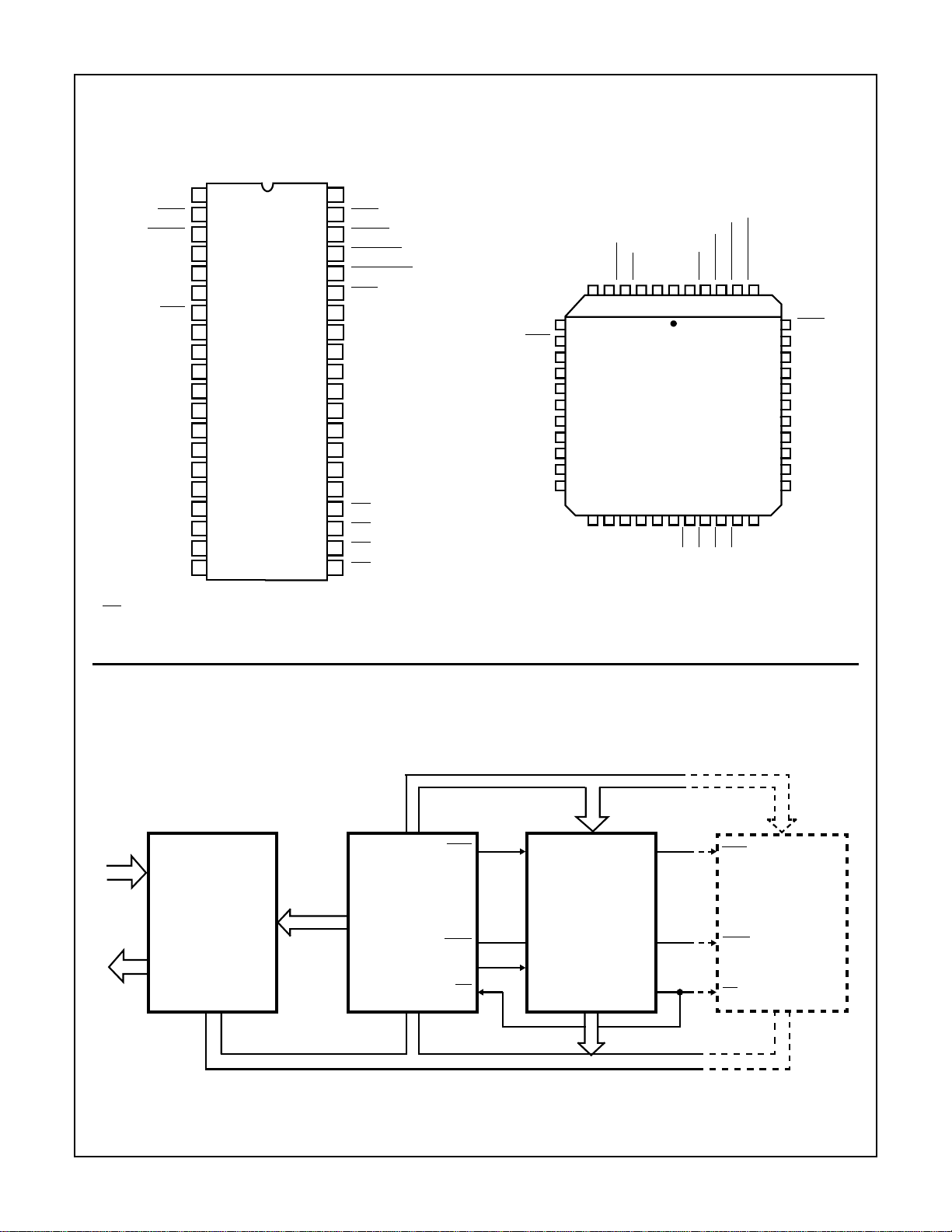
FIGURE 1. TYPICAL CDP1805AC, CDP1806AC SMALL MICROPROCESSOR SYSTEM
CONTROL
MA0 - MA7
CDP1805AC WITH
RAM, COUNTER/TIMER
CDP1806AC WITH
COUNTER/TIMER
BUS0 - BUS7
MRD
MWR
TPA
ME
TPA
(CDP1805AC ONLY)
8-BIT DATA BUS
ADDRESS BUS
MA0 - MA7
CDP1833
1K BYTE ROM
BUS0 - BUS7
CEO
MA0-MA4
MRD
CDP1824
32 BYTE RAM
(USED WITH
CDP1806AC ONLY)
MWR
CS
BUS0-BUS4
3-39
CONTROL
CLEAR WAIT
CLOCK
CDP1805AC, CDP1806AC
STATE
CODES
SYSTEM
TIMING
XTAL
SCI
Q LOGIC
TPA
TPB
MWR
SCO
MRD
TC
DECODE
INSTRUCTION
I/O
COMMANDS
N0N1N2
N
(4)
I
(4)
P
(4)
INTIN
OUT
DMA
DMA
I/O REQUESTS
EF4
EF3
EF2
I/O FLAGS
EF1
MA0
MA1
MA2
MA3
MA4
MA5
MA6
MA7
MEMORY ADDRESS LINES
ME FOR CDP1805AC
LOGIC
CLOCK
TIMING LOGIC
CONTROL AND
INTERRUPT
LOGIC
ARRAY
REGISTER
A
(16)
MUX
EF1
EF2
TPA
÷ 32
INCR/
DF
ALU
B
(8)D(8)
DECR
(1)
MODE
CONTROL
CLK
FOR CDP1806AC
DD
V
RAM
64-BYTE
REGISTER (CH)
COUNTER HOLDING
8-BIT
COUNTER/TIMER
R
R(0).0
R(1).0
R(0).1
R(1).1
T
X
LATCH
R(2).0
R(2).1
(8)
(4)
AND
DECODE
R(9).0
R(9).1
R(A).0
R(A).1
R(F).0
R(E).0
R(F).1
R(E).1
8-BIT BIDIRECTIONAL DATA BUS
ONLY
CDP1805AC
BUS 0
BUS 1
BUS 2
BUS 3
BUS 4
BUS 5
BUS 6
BUS 7
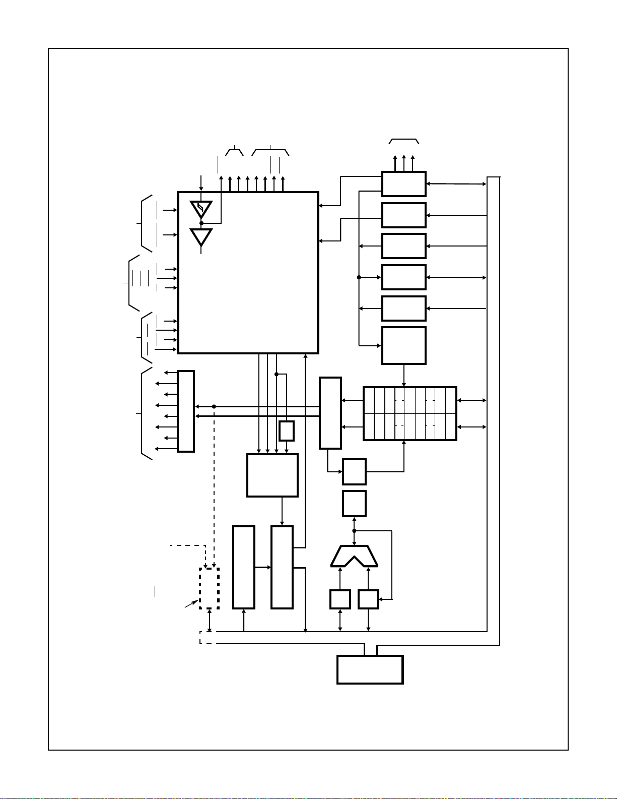
FIGURE 2. BLOCK DIAGRAM FOR CDP1805AC AND CDP1806AC
3-40
CDP1805AC, CDP1806AC
Absolute Maximum Ratings Thermal Information
DC Supply Voltage Range, (VDD)
(All Voltages Referenced to VSS Terminal). . . . . . . . . -0.5V to +7V
Input Voltage Range, All Inputs . . . . . . . . . . . . . -0.5V to VDD +0.5V
DC Input Current, any One Input. . . . . . . . . . . . . . . . . . . . . . . . .±10mA
CAUTION: Stresses above those listed in “Absolute Maximum Ratings” may cause permanent damage to the device. This is a stress only rating and operation
of the device at these or any other conditions above those indicated in the operational sections of this specification is not implied.
Thermal Resistance (Typical, Note 2) θJA (oC/W) θJC (oC/W)
PDIP Package. . . . . . . . . . . . . . . . . . . 50 N/A
PLCC Package . . . . . . . . . . . . . . . . . . 46 N/A
SBDIP Package. . . . . . . . . . . . . . . . . . 55 15
Device Dissipation Per Output Transistor
TA = Full Package Temperature Range . . . . . . . . . . . . . . 100mW
Operating Temperature Range (TA)
Package Type D. . . . . . . . . . . . . . . . . . . . . . . . . .-55oC to +125oC
Package Type E and Q . . . . . . . . . . . . . . . . . . . . .-40oC to +85oC
Storage Temperature Range (T
). . . . . . . . . . . .-65oC to +150oC
STG
Lead Temperature (During Soldering)
At Distance 1/16 ±1/32in (1.59 ±0.79mm) from case for
10s Max . . . . . . . . . . . . . . . . . . . . . . . . . . . . . . . . . . . . . .+265oC
Printed Circuit Board Mount: 57mm x 57mm Minimum Area x
1.6mm Thick G10 Epoxy Glass, or Equivalent.
Recommended Operating Conditions T
= Full-Package Temperature Range. For maximum reliability, operating conditions
A
should be selected so that operation is always within the following ranges.
CDP1805ACD, CDP1805ACE
PARAMETER
TEST CONDITIONS
V
DD
(V)
CDP1806ACD, CDP1806ACE
UNITSMIN MAX
DC Operating Voltage Range - 4 6.5 V
Input Voltage Range - V
Minimum Instruction Time (Note 1)
5 3.2 - µs
SS
V
DD
V
(fCL = 5MHz)
Maximum DMA Transfer Rate 5 - 0.625 Mbyte/s
Maximum Clock Input Frequency,
5 DC 5 MHz
Load Capacitance (CL) = 50pF
Maximum External Counter/Timer Clock
5 DC 2 MHz
Input Frequency to EF1, EF2
NOTES:
1. Equals 2 machine cycles - one Fetch and one Execute operation for all instructions except Long Branch, Long Skip, NOP, and “68” family
instructions, which are more than two cycles.
2. θJA is measured with the component mounted on an evaluation PC board in free air.
Static Electrical Specifications at T
= -40oC to +85oC, VDD±5%, Except as Noted
A
CDP1805ACD, CDP1805ACE
CDP1806ACD, CDP1806ACE
PARAMETER
Quiescent Device Current, I
DD
Output Low Drive (Sink) Current, (Except XTAL), I
XTAL Output, I
OL
Output High Drive (Source) Current (Except XTAL, I
XTAL, I
OH
Output Voltage Low Level, V
Output Voltage High Level, V
OL
OH
OL
OH
V
(V)
O
V
(V)
V
IN
DD
(V)
(NOTE 3)
TYP MAX
UNITSMIN
- 0, 5 5 - 50 200 µA
0.4 0, 5 5 1.6 4 - mA
0.4 5 5 0.2 0.4 - mA
4.6 0, 5 5 -1.6 -4 - mA
4.6 0 5 -0.1 -0.2 - mA
- 0, 5 5 - 0 0.1 V
- 0, 5 5 4.9 5 - V
3-41
CDP1805AC, CDP1806AC
Static Electrical Specifications at T
= -40oC to +85oC, VDD±5%, Except as Noted (Continued)
A
CDP1805ACD, CDP1805ACE
CDP1806ACD, CDP1806ACE
PARAMETER
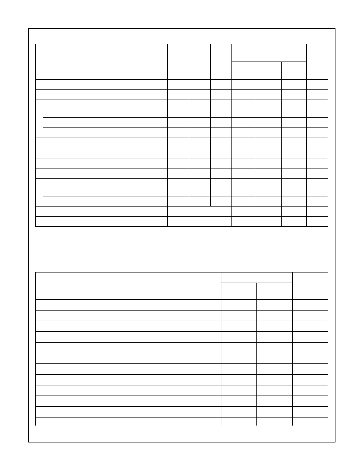
Input Low Voltage (BUS0 - BUS7, ME), V
Input High Voltage (BUS0 - BUS7, ME), V
V
O
(V)
IL
IH
0.5, 4.5 - 5 - - 1.5 V
0.5, 4.5 - 5 3.5 - - V
V
(V)
V
IN
DD
(V)
(NOTE 3)
TYP MAX
Schmitt Trigger Input Voltage (Except BUS0 - BUS7, ME)
Positive Trigger Threshold, V
Negative Trigger Threshold, V
Hysteresis, V
H
Input Leakage Current, I
P
N
IN
Three-State Output Leakage Current, I
Input Capacitance, C
Output Capacitance, C
IN
OUT
OUT
0.5, 4.5 - 5 2.2 2.9 3.6 V
0.5, 4.5 - 5 0.9 1.9 2.8 V
0.5, 4.5 - 5 0.3 0.9 1.6 V
- 0, 5 5 - ±0.1 ±5 µA
0, 5 0, 5 5 - ±0.2 ±5 µA
- - - - 5 7.5 pF
---- 1015pF
Total Power Dissipation (Note 4)
Run - - 5 - 35 50 mW
Idle “00” at M (0000) - - 5 - 12 18 mW
Minimum Data Retention Voltage, V
Data Retention Current, I
DR
DR
VDD = V
DR
- 2 2.4 V
VDD = 2.4 - 25 100 µA
NOTES:
3. Typical values are for TA = +25oC and nominal VDD.
4. External clock: f = 5MHz, tR, tF = 10ns; CL = 50pF.
UNITSMIN
Dynamic Electrical Specifications at T
VDD-0.1V; VDD = 5V, ±5%.
PARAMETER
Propagation Delay Times
Clock to TPA, TPB, t
Clock-to-Memory High-Address Byte, t
Clock-to-Memory Low-Address Byte, t
Clock to MRD, t
Clock to MWR, t
PLH
PLH
Clock to (CPU DATA to BUS), t
Clock to State Code, t
Clock to Q, t
Clock to N, t
PLH
PLH
, t
Clock to Internal RAM Data to BUS, t
Minimum Set-Up And Hold Times (Note 2)
, t
PLH
PHL
, t
PLH
PHL
, t
PLH
PHL
, t
PHL
, t
(See Note 5) 150 275 ns
PHL
, t
PLH
PHL
, t
PLH
PHL
, t
PHL
PHL
, t
PLH
PHL
= -40o to +85oC; CL = 50pF; Input tR, tF = 10ns; Input Pulse Levels = 0.1V to
A
CDP1805AC CDP1806AC
(NOTE 5)
TYP MAX
150 275 ns
325 550 ns
275 450 ns
200 325 ns
375 625 ns
225 400 ns
250 425 ns
250 425 ns
420 650 ns
UNITS
3-42
CDP1805AC, CDP1806AC
Dynamic Electrical Specifications at T
= -40o to +85oC; CL = 50pF; Input tR, tF = 10ns; Input Pulse Levels = 0.1V to
A
VDD-0.1V; VDD = 5V, ±5%. (Continued)
PARAMETER
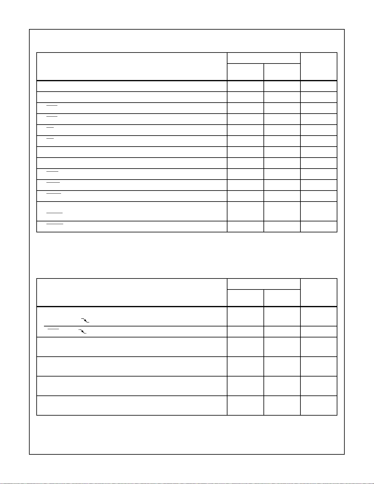
Data Bus Input Set-Up, t
Data Bus Input Hold, t
DMA Set-Up, t
DMA Hold, t
ME Set-Up, t
ME Hold, t
SU
H
SU
H
Interrupt Set-Up, t
Interrupt Hold, t
WAIT Set-Up, t
EF1-4 Set-Up, t
EF1 -4 Hold, t
H
SU
SU
H
SU
H
SU
Minimum Pulse Width Times (Note 6)
CLEAR Pulse Width, t
CLOCK Pulse Width, t
WL
W
NOTES:
5. Typical values are for TA = 25o C and nominal V
DD
.
6. Maximum limits of minimum characteristics are the values above which all devices function.
CDP1805AC CDP1806AC
(NOTE 5)
TYP MAX
UNITS
-100 0 ns
125 225 ns
-75 0 ns
100 175 ns
125 320 ns
050ns
-100 0 ns
100 175 ns
20 50 ns
-125 0 ns
175 300 ns
100 175 ns
75 100 ns
Timing Specifications as a function of T (T =
1
/f
) at TA = -40 to +85oC, VDD = 5V, ±15%
CLOCK
CDP1805AC, CDP1806AC
(NOTE 7)
PARAMETER
MAX
High-Order Memory-Address Byte
Set-Up to TPA Time, t
MRD to TPA Time, t
SU
SU
2T-275 2T -175 ns
T/2 -100 T/2 -75 ns
High-Order Memory-Address Byte
Hold after TPA Time, t
H
T/2 +75 T/2 +100 ns
Low-Order Memory-Address Byte
Hold after WR Time, t
H
T +180 T +240 ns
CPU Data to Bus
Hold after WR Time, t
H
Required Memory Access Time, t
ACC
T +110 T +150 ns
Address to Data 4.5T -440 4.5T -330 ns
NOTE:
7. Typical values are for TA = +25oC and nominal VDD.
UNITSTYP
3-43
CDP1805AC, CDP1806AC
Timing Waveforms For Possible Operating Modes
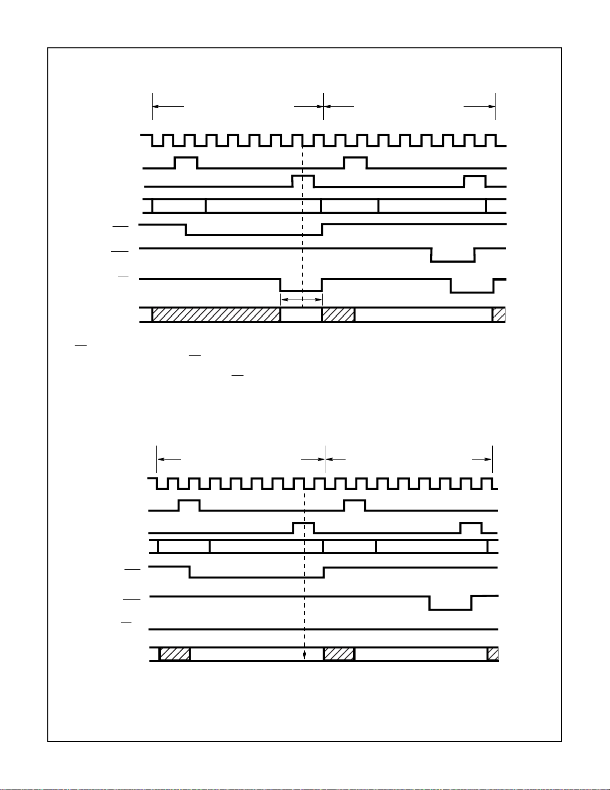
INTERNAL RAM READ CYCLE INTERNAL RAM WRITE CYCLE
00 10 20 30 40 50 60 70 00 10 20 30 40 50 60 70
CLOCK
01 11 21 31 41 51 61 71 01 11 21 31 41 51 61 71
TPA
TPB
MEMORY
ADDRESS
MRD
MWR
†
ME
DAT A
BUS
IN
HIGH BYTE LOW BYTE HIGH BYTE LOW BYTE
VALID DATA FROM MEMORY
VALID DATA FROM CPU
NOTE:
8. ME has a minimum setup and hold time with respect to the beginning of clock 70. For a memory read operation, RAM data will appear
on the data bus during the time ME is active after clock 31. The time shown can be longer, if for instance, a DMA out operation is performed on internal RAM data, to allow data enough time to be latched into an external device. The internal RAM is automatically deselected at the end of clock 71 independent of ME.
† For CDP1805AC only.
FIGURE 3. INTERNAL MEMORY OPERATION TIMING WAVEFORMS
EXTERNAL MEMORY READ CYCLE EXTERNAL MEMORY WRITE CYCLE
00 10 20 30 40 50 60 70 00 10 20 30 40 50 60 70
CLOCK
TPA
01 11 21 31 41 51 61 71 01 11 21 31 41 51 61 71
TPB
MEMORY
ADDRESS
MRD
MWR
ME IN
†
(HIGH)
DAT A
BUS
NOTE:
† For CDP1805AC only.
HIGH BYTE LOW BYTE LOW BYTEHIGH BYTE
DATA LATCHED IN CPU VALID DATA FROM CPU
FIGURE 4. EXTERNAL MEMORY OPERATION TIMING WAVEFORMS
3-44
CDP1805AC, CDP1806AC
CLOCK
TPA
TPB
MEMORY
ADDRESS
MRD
(MEMORY
READ CYCLE)
MWR
(MEMORY
WRITE CYCLE)
† ME
(MEMORY
ENABLE)
†† EMS
(EXTERNAL
MEMORY
SELECT)
DATA FROM
CPU TO BUS
DATA FROM
INTERNAL MEMORY
TO BUS (
ME = LOW)
t
W
1 2 3 4 5 6 7 0
00 01 10 11 20 21 30 31 40 41 50 51 60 61 70071 00 01
t
PLH,tPHL
t
PLH
t
PLH,
t
PHL
t
PLH
HIGH ORDER
ADDRESS BYTE
t
PLH,
t
PHL
t
PHL
t
t
PLH,tPHL
t
SU
t
t
PHL
SU
t
H
LOW ORDER
ADDRESS BYTE
IS ALLOWABLE
t
SU
INTERNAL RAM
ACCESS TIME
t
PLH
t
PHL
t
PHL
t
PHL
PLH
t
SU
t
PLH
t
PLH
t
t
PHL
t
H
t
PHL
H
t
H
t
PLH,tPLH
t
t
SU
t
SUtH
PLH,tPHL
t
SU
t
H
t
H
t
SU
H
SAMPLED END OF S0
FLAG LINES
t
SU
STATE CODES
N0, N1, N2
(I/O EXECUTION
CYCLE)
DATA FROM
BUS TO CPU
DMA REQUEST
INTERRUPT
REQUEST
EF1 - EF4
Q
t
PLH
t
PLH,tPHL
DATA LATCHED
IN CPU
DMA SAMPLED (S1, S2, S3)
INTERRUPT
SAMPLED (S1, S2)
t
SUtH
t
WAIT
t
CLEAR
WL
NOTES:
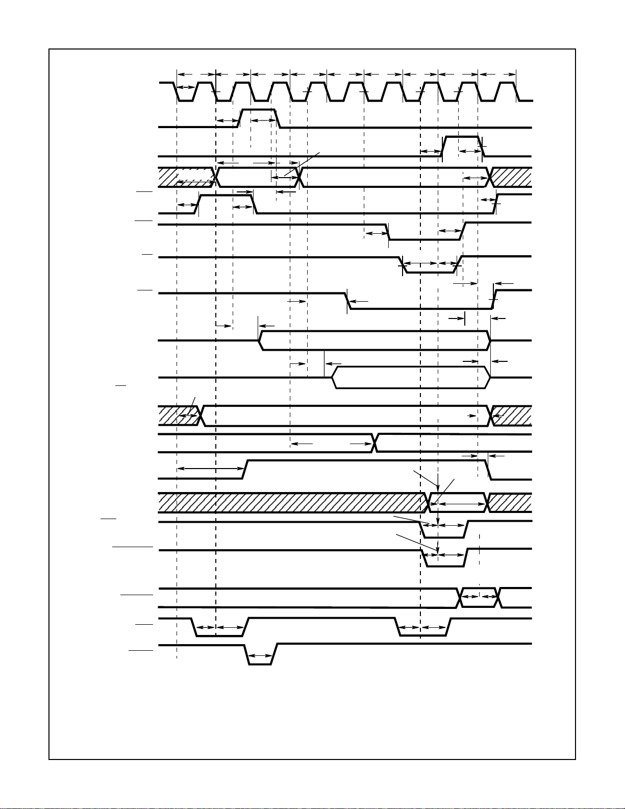
† This Timing Diagram is used to show signal relationships only, and does not represent any specific machine cycle.
† All measurements are referenced to 50% point of the wave forms.
† Shaded areas indicate “don’t care” or undefined state. Multiple transitions may occur during this period.
† For the run (RAM only) mode only.
†† For the run (RAM/ROM) mode only.
FIGURE 5. TIMING WAVEFORMS
t
PHL
t
H
3-45
CDP1805AC, CDP1806AC
Enhanced CDP1805AC and CDP1806AC
Operation
Timing
Timing for the CDP1805AC and CDP1806AC is the same as
the CDP1802 microprocessor series, with the following
exceptions:
• 4.5 Clock Cycles Are Provided for Memory Access Instead
of 5.
• Q Changes 1/2 Clock Cycle Earlier During the SEQ and
REQ Instructions.
• Flag Lines (
Cycle Instead of at the Beginning of the S1 Cycle.
• Pause Can Only Occur on the Low-To-High Transition of
Either TPA or TPB, Instead of any Negative Clock Transition.
Special Features
Schmitt triggers are provided on all inputs, except
BUS 0-BUS 7, for maximum immunity from noise and slow
signal transitions. A Schmitt Trigger in the oscillator section
allows operation with an RC or crystal.
The CDP1802 Series LOAD mode is not retained. This
mode (
and CDP1806AC.
A low power mode is provided, which is initiated via the IDLE
instruction. In this mode all external signals, except the oscillator, are stopped on the low-to-high transition of TPB. All
outputs remain in their previous states,
“1”, and the data bus floats. The IDLE mode is exited by a
DMA or INT condition. The INT includes both external interrupts and interrupts generated by the Counter/Timer. The
only restrictions are that the Timer mode, which uses the
TPA ÷ 32 clock source, and the underflow condition of the
Pulse Width Measurement modes are not available to exit
the IDLE mode.
EF1-EF4) Are Sampled at the End of the S0
ME and
WAIT, CLEAR = 0) is not allowed on the CDP1805AC
MRD is set to a logic
MRD = VDD: Input data from I/O to CPU and memory.
MRD = VSS: Output data from Memory to I/O.
EF1 to EF4 (4 Flags)
These inputs enable the I/O controllers to transfer status
information to the processor. The levels can be tested by the
conditional branch instructions. They can be used in conjunction with the INTERRUPT request line to establish interrupt priorities. The flag(s) are sampled at the end of every S0
cycle.
EF1 and EF2 are also used for event counting and
pulse width measurement in conjunction with the
Counter/Timer.
INTERRUPT, DMA-IN, DMA-OUT (3 I/O Requests)
DMA-lN and DMA-OUT are sampled during TPB every S1,
S2, and S3 cycle.
INTERRUPT is sampled during TPB ev ery
S1 and S2 cycle.
Interrupt Action - X and P are stored in T after executing
current instruction; designator X is set to 2; designator P is
set to 1; interrupt enable (MIE) is reset to 0 (inhibit); and
instruction execution is resumed. The interrupt action
requires one machine cycle (S3).
DMA Action - Finish executing current instruction; R(0)
points to memory area for data transfer; data is loaded into
or read out of memory; and R(0) is incremented.
NOTE: In the event of concurrent DMA and INTERRUPT requests,
DMA-IN has priority followed by DMA-OUT and then INTERRUPT.
(The interrupt request is not internally latched and must be held true
after DMA).
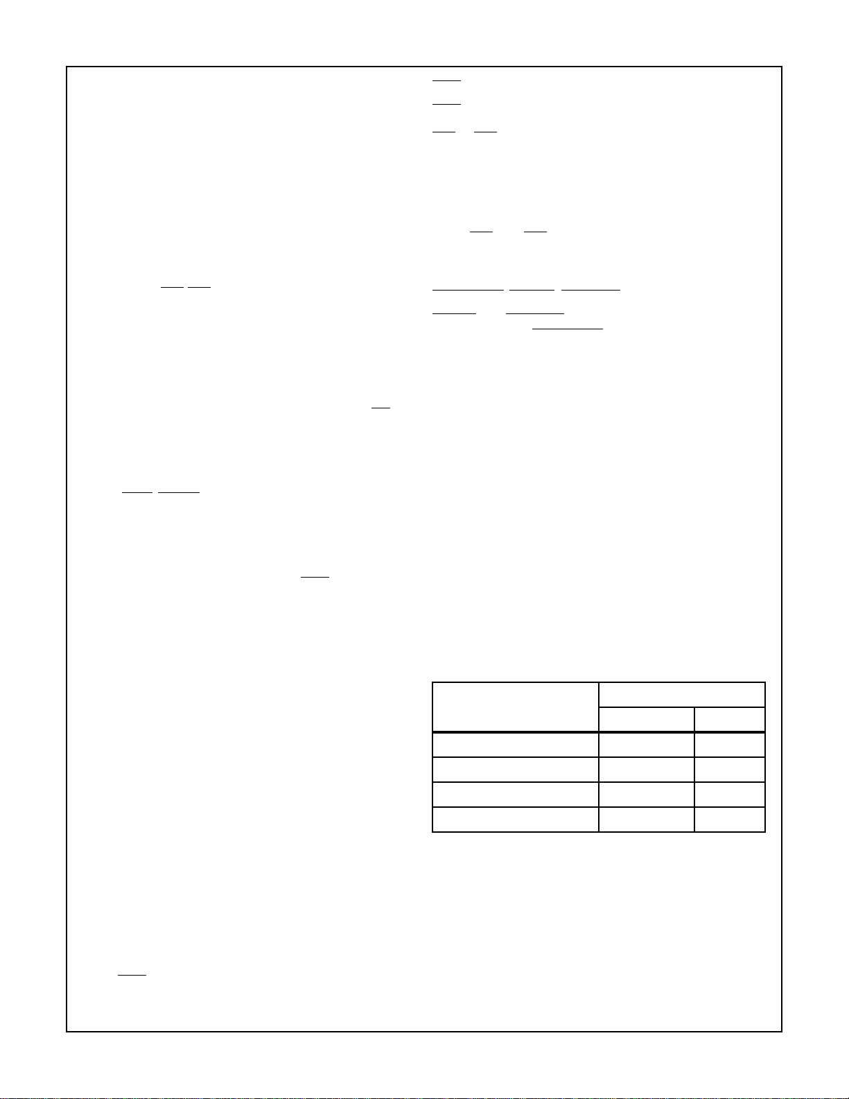
SC0, SC1, (2 State Code Lines)
These outputs indicate that the CPU is: 1) fetching an
instruction, or 2) executing an instruction, or 3) processing a
DMA request, or 4) acknowledging an interrupt request. The
levels of state code are tabulated below. All states are valid
at TPA.
STATE CODE LINES
Signal Descriptions
Bus 0 to Bus 7 (Data Bus)
8-Bit bidirectional DATA BUS lines. These lines are used for
transferring data between the memory, the microprocessor,
and I/O devices.
N0 to N2 (I/O) Lines
Activated by an I/O instruction to signal the I/O control logic
of a data transfer between memory and I/O interface. These
lines can be used to issue command codes or device selection codes to the I/O devices. The N-bits are low at all times
except when an I/O instruction is being executed. During this
time their state is the same as the corresponding bits in the
N Register. The direction of data flow is defined in the I/O
instruction by bit N3 (internally) and is indicated by the level
of the
MRD Signal:
STATE TYPE
S0 (Fetch) L L
S1 (Execute) L H
S2 (DMA) H L
S3 (Interrupt) H H
NOTE: H = VDD, L = V
SS.
SC1 SC0
TPA, TPB (2 Timing Pulses)
Positive pulses that occurrence in each machine cycle (TPB
follows TPA). They are used by I/O controllers to interpret
codes and to time interaction with the data bus. The trailing
edge of TPA is used by the memory system to latch the highorder byte of the multiplexed 16-bit memory address.
3-46
 Loading...