

Page 1
3-3
TM
Features
• Maximum Input Clock Maximum Frequency Options
At V
DD
= 5V
- CDP1802A, AC . . . . . . . . . . . . . . . . . . . . . . . . .3.2MHz
- CDP1802BC . . . . . . . . . . . . . . . . . . . . . . . . . . .5.0MHz
• Maximum Input Clock Maximum Frequency Options
At VDD = 10V
- CDP1802A, AC . . . . . . . . . . . . . . . . . . . . . . . . .6.4MHz
• Minimum Instruction Fetch-Execute Times
At V
DD
= 5V
- CDP1802A, AC . . . . . . . . . . . . . . . . . . . . . . . . . . 5.0µs
- CDP1802BC . . . . . . . . . . . . . . . . . . . . . . . . . . . . 3.2µs
• Any Combination of Standard RAM and ROM Up to
65,536 Bytes
•8
-Bit Parallel Organization With Bid irectional Dat a Bus
and Multiplexed Address Bus
• 16 x 16 Matrix of Registers for Use as Multiple
Program Counters, Data Pointers, or Data Registers
•On
-Chip DMA, Interrupt, and Flag Inputs
• Program mable Single
-Bit Output Port
• 91 Easy
-to-Use Instruc tions
Description
The CDP1802 family of CMOS microprocessors are 8-bit
register oriented central processing units (CPUs) designed
for use as general purpose computing or control elements in
a wide range of stored program systems or products.
The CDP1802 types include all of the circuits required for
fetching, interpreting, and executing instructions which have
been stored in standard types of memories. Extensive
input/output (I/O) control features are also provided to facilitate system design.
The 1800 series architecture is designed with emphasis on
the total microcomputer system as an integral entity so that
systems having maximum flexibility and minimum cost can
be realized. The 1800 series CPU also provides a synchronous interface to memories and external controllers for I/O
devices, and minimizes the cost of interface controllers. Further, the I/O interface is capable of supporting devices operating in polled, interrupt driven, or direct memory access
modes.
The CDP1802A and CDP1802AC have a maximum input
clock frequency of 3.2M Hz at V
DD
= 5V. The CDP1802A and
CDP1802AC are functionally identical. They differ in that the
CDP1802A has a recommended operating voltage range of
4V to 10.5V, and the CDP1802AC a recommended operating voltage range of 4V to 6.5V.
The CDP1802BC is a higher speed version of the
CDP1802AC, having a maximum input clock frequency of
5.0MHz at V
DD
= 5V, and a recommended operating voltage
range of 4V to 6.5V.
Ordering Information
PART NUMBER
TEMPERATURE RANGE PACKAGE PKG. NO.5V - 3.2MHz 5V - 5MHz
CDP1802ACE CDP1802BCE -40
o
C to +85oC PDIP E40.6
CDP1802ACEX CDP1802BCEX Burn-In E40.6
CDP1802ACQ CDP1802BCQ -40
o
C to +85oC PLCC N44.65
CDP1802ACD - -40
o
C to +85oC SBDIP D40.6
CDP1802ACDX CDP1802BCDX Burn-In D40.6
March 1997
File Number
1305.2
CDP1802A, CDP1802AC,
CDP1802BC
CMOS 8-Bit Microprocessors
CAUTION: These devices are sensitive to electrostatic discharge; follow proper IC Handling Procedures.
1-888-INTERSIL or 321-724-7143
| Intersil (and design) is a trademark of Intersil Americas Inc.
Copyright © Intersil Americas Inc. 2002. All Rights Reserved
Page 2
3-4
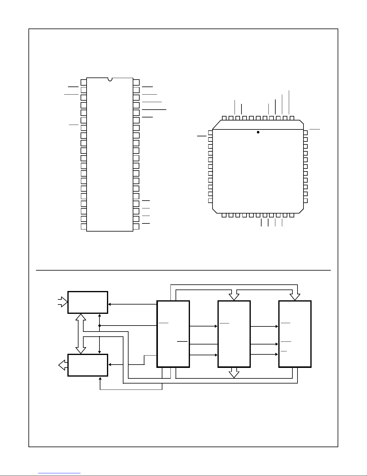
Pinouts
40 LEAD PDIP (PACK AGE SUFFIX E)
40 LEAD SBDIP (PACKAGE SUFFIX D)
TOP VIEW
44 LEAD PLCC
(PACKAGE TYPE Q)
TOP VIEW
FIGURE 1. TYPICAL CDP1802 SM ALL MI CRO PROC E SS OR SYST E M
13
1
2
3
4
5
6
7
8
9
10
11
12
14
15
16
17
18
19
20
CLOCK
WAIT
CLEAR
Q
SC1
SC0
MRD
BUS 7
BUS 6
BUS 5
BUS 4
BUS 3
BUS 2
BUS 1
BUS 0
V
CC
N2
N1
N0
V
SS
28
40
39
38
37
36
35
34
33
32
31
30
29
27
26
25
24
23
22
21
V
DD
XTAL
DMA IN
DMA OUT
INTERRUPT
MWR
TPA
TPB
MA7
MA6
MA5
MA4
MA3
MA2
MA1
MA0
EF1
EF2
EF3
EF4
44 43 42 41 40
39
38
37
36
35
34
33
32
31
30
29
2827
123456
262524232221201918
7
8
9
10
11
12
13
14
15
16
17
SC0
MRD
BUS 7
BUS 6
BUS 5
NC
BUS 4
BUS 3
BUS 2
BUS 1
BUS 0
SC1QCLEAR
WAIT
CLOCKNCVDDXTAL
DMA-IN
DMA-OUT
INTERRUPT
V
CC
N2N1N0
V
SS
NC
EF4
EF3
EF2
EF1
MA0
MWR
TPA
TPB
MA7
MA6
NC
MA5
MA4
MA3
MA2
MA1
CDP1852
INPUT PORT
DATA CS1
CS2
CDP1852
OUTPUT
PORT
CLOCK
CS1
CS2
MA0-7
N0
MRD
MWR
N1
TPB
DATA
TPA
CDP1802
8
-BIT CPU
MRD
MA0-4
MWR
CS
CDP1824
32 BYTE RAM
MA0-7
DATA
CDP1833
1K
-ROM
CEOTPA
MRD
ADDRESS BUS
CDP1802A, CDP1802AC, CDP1802BC
Page 3
3-5
Block Diagram
FIGURE 2.
MUX
MA7MA5MA3MA1
MA0MA2MA4MA6
MEMORY ADDRESS LINES I/O FLAGS
ALU
B
D
DF
INCR/
DECR
A
R(0).1 R(0).0
R(1).0R(1).1
R(2).1 R(2).0
R(9).0
R(A).0R(A).1
R(9).1
R(E).1
R(F).1 R(F).0
R(E).0
REGISTER
ARRAY
8-BIT BIDIRECTIONAL DATA BUS
LATCH
AND
DECODE
R
XTPIN
N1
N0
N2
I/O
COMMANDS
BUS 0
BUS 1
BUS 2
BUS 3
BUS 4
BUS 5
BUS 6
BUS 7
TO INSTRUCTION
DECODE
CONTROL AND
TIMING LOGIC
CLOCK
LOGIC
I/O REQUESTS
CONTROL
EF1
EF3
EF2 EF4
DMA
OUT
DMA
IN INT
CLEAR
WAIT
CLOCK
XTAL
SCO
SCI
Q LOGIC
TPA
TPB
MWR
MRD
SYSTEM
STATE
CODES
TIMING
CDP1802A, CDP1802AC, CDP1802BC
Page 4
3-6
Absolute Maximum Ratings Thermal Information
DC Supply Voltage Range, (VDD)
(All Voltages Referenced to V
SS
Terminal)
CDP1802A. . . . . . . . . . . . . . . . . . . . . . . . . . . . . . . . . -0.5V to +11V
CDP1802AC, CDP1802BC . . . . . . . . . . . . . . . . . . . . -0.5V to +7V
Input Voltage Range, All Inputs . . . . . . . . . . . . . .-0.5V to V
DD
+0.5V
DC Input Current, any One Input. . . . . . . . . . . . . . . . . . . . . . . . .±10mA
Thermal Resistance (Typical, Note 4) θ
JA
(oC/W) θJC (oC/W)
PDIP . . . . . . . . . . . . . . . . . . . . . . . . . . 50 N/A
PLCC. . . . . . . . . . . . . . . . . . . . . . . . . . 46 N/A
SBDIP . . . . . . . . . . . . . . . . . . . . . . . . . 55 15
Device Dissipation Per Output Transistor
T
A
= Full Package Temperature Range. . . . . . . . . . . . . . . 100mW
Operating Temperature Range (T
A
)
Package Type D . . . . . . . . . . . . . . . . . . . . . . . . . .-55
o
C to +125oC
Package Type E and Q. . . . . . . . . . . . . . . . . . . . . . -40
o
C to +85oC
Storage Temperature Range (T
STG
) . . . . . . . . . . . . -65oC to +150oC
Lead Temperature (During Soldering)
At distance 1/16 ± 1/32 In. (1.59 ± 0.79mm)
from case for 10s max. . . . . . . . . . . . . . . . . . . . . . . . . . . . +265
o
C
Lead Tips Only. . . . . . . . . . . . . . . . . . . . . . . . . . . . . . . . . . +300
o
C
CAUTION: Stresses above t hos e l iste d in “Absolute Maximum Ra tings” may cause permanent d am age to th e d evi ce . T his i s a stre ss o nl y rating and operatio n
of the device at these or any other conditions above those in dica ted in the operational sections of this specification is not implied.
Recommended Operating Conditions T
A
= -40oC to +85oC. For maximum reliability, operating conditions should be selected so
that operation is always within the following ranges:
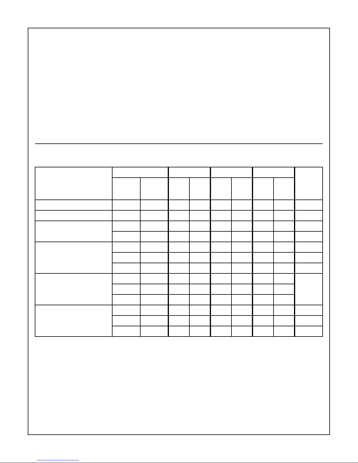
PARAMETER
TEST CONDITIONS CDP1802A CDP1802AC CDP1802BC
UNITS
(NOTE 2)
V
CC
(V)
V
DD
(V) MIN MAX MIN MAX MIN MAX
DC Operating Voltage Range - - 4 10.5 4 6.5 4 6.5 V
Input Voltage Range - - V
SS
V
DD
V
SS
V
DD
V
SS
V
DD
V
Maximum Clock Input Rise or
Fall Time
4 to 6.5 4 to 6.5 - - - 1 - 1 µs
4 to 10.5 4 to 10.5 - 1 - - - - µs
Minimum Instruction
Time
(Note 3)
5 5 5-5-3.2- µs
5 10 4----- µs
10 10 2.5 - - - - - µs
Maximum DMA Transfer Rate 5 5 - 400 - 400 - 667 KBytes/s
5 10 -500----
10 10 - 800 - - - -
Maximum Clock Input Frequency,
f
CL
, Load Capacitance
(C
L
) = 50pF
5 5 DC 3.2 DC 3.2 DC 5 M Hz
5 10DC4----MHz
10 10 DC 6.4 - - - - MHz
NOTES:
1. Printed circuit board mount: 57mm x 57mm minimum area x 1.6mm thick G10 epoxy glass, or equivalent.
2. V
CC
must never exceed VDD.
3. Equals 2 machine cycles - one Fetch and one Execute operation for all instructions except Long Branch and Long Skip, which require 3
machine cycles - one Fetch and two Execute operations.
4. θ
JA
is measured with component mounted on an evaluation board in free air.
CDP1802A, CDP1802AC, CDP1802BC
Page 5
3-7
Static Electrical Specifications at T
A
= -40oC to +85oC, Except as Noted
PARAMETER SYMBOL
TEST CONDITIONS CDP1802A
CDP1802AC,
CDP1802BC
UNITS
V
OUT
(V)
V
IN
(V)
V
CC
,
V
DD
(V) MIN
(NOTE 1)
TYP MAX MIN
(NOTE 1)
TYP MAX
Quiescent Device Current I
DD
- - 5 - 0.1 50 - 1 200 µA
- - 10 - 1 200 - - - µA
Output Low Drive (Sink)
Current I
OL
0.4 0, 5 5 1.1 2.2 - 1.1 2.2 - mA
(Except XTAL
) 0.5 0, 10 10 2.2 4.4 - - - - mA
XTAL
0.4 5 5 170 350 - 1 70 350 - µA
Output High Drive (Source)
Current I
OH
4.6 0, 5 5 -0.27 -0.55 - -0.27 -0.55 - mA
(Except XTAL
) 9.5 0, 10 10 -0.55 -1.1 - - - - mA
XTAL
4.6 0 5 -125 -250 - -125 -250 - µA
Output Voltage - 0, 5 5 - 0 0.1 - 0 0.1 V
Low Level V
OL
- 0, 10 10 - 0 0.1 - - - V
Output Voltage - 0, 5 5 4.9 5 - 4.9 5 - V
High Level V
OH
- 0, 10 10 9.9 10 - - - - V
Input Low Voltage V
IL
0.5, 4.5 - 5 - - 1.5 - - 1.5 V
0.5, 4.5 - 5, 10 - - 1 - - - V
1, 9-10--3---V
Input High Voltage V
IH
0.5, 4.5 - 5 3.5 - - 3.5 - - V
0.5, 4.5 - 5, 10 4 - - - - - V
1, 9-107-----V
CLEAR
Input Voltage V
H
- - 5 0.4 0.5 - 0.4 0.5 - V
Schmitt Hysteresis - - 5, 10 0.3 0.4 - - - - V
- - 10 1.5 2 - - - - V
Input Leakage Current I
IN
Any
Input
0, 5 5 - ±10
-4
±1-±10
-4
±1 µA
0, 10 10 - ±10
-4
±1---µA
Three-State Output Leakage I
OUT
0, 5 0, 5 5 - ±10
-4
±1-±10
-4
±1 µA
Current 0, 10 0, 10 10 - ±10
-4
±1---µA
Operating Current
CDP1802A, AC
at f = 3.2MHz
I
DDI
(Note 2)
--5-24-24mA
CDP1802BC
at f = 5.0MHz
--5----36mA
Minimum Data Retention
Voltage
V
DR
VDD = V
DR
-22.4- 22.4V
Data Retention Current I
DR
VDD = 2.4V - 0.05 - - 0.5 - µA
CDP1802A, CDP1802AC, CDP1802BC
Page 6
3-8
Input Capacitance C
IN
- 5 7.5 - 5 7.5 pF
Output Capacitance C
OUT
- 10 15 - 10 15 pF
NOTES:
1. Typical values are for T
A
= +25oC and nominal VDD.
2. Idle “00” at M(0000), C
L
= 50pF.
Dynamic Electrical Specifications T
A
= -40oC to +85oC, CL = 50pF, VDD ±5%, Except as Noted
PARAMETER SYMBOL
TEST
CONDITIONS
CDP1802A,
CDP1802AC CDP1802BC
UNITSV
CC
(V) VDD (V)
(NOTE 1)
TYP MAX
(NOTE 1)
TYP MAX
PROPAGATION DELAY TIMES
Clock to TPA, TPB t
PLH
, t
PHL
5 5 200 300 200 300 ns
5 10 150 250 - - ns
10 10 100 150 - - ns
Clock-to-Memory High-Address Byte t
PLH
, t
PHL
5 5 600 850 475 525 ns
5 10 400 600 - - ns
10 10 300 400 - - ns
Clock-to-Memory Low-Address Byte Valid t
PLH
, t
PHL
5 5 250 350 175 250 ns
5 10 150 250 - - ns
10 10 100 150 - - ns
Clock to MRD
t
PHL
5 5 200 300 175 275 ns
5 10 150 250 - - ns
10 10 100 150 - - ns
Clock to MRD
t
PLH
5 5 200 350 175 275 ns
5 10 150 290 - - ns
10 10 100 175 - - ns
Clock to MWR
t
PLH
, t
PHL
5 5 200 300 175 225 ns
5 10 150 250 - - ns
10 10 100 150 - - ns
Clock to (CPU DATA to BUS) Val id t
PLH
, t
PHL
5 5 300 450 250 375 ns
5 10 250 350 - - ns
10 10 100 200 - - ns
Static Electrical Specifications at T
A
= -40oC to +85oC, Except as Noted (Continued)
PARAMETER SYMBOL
TEST CONDITIONS CDP1802A
CDP1802AC,
CDP1802BC
UNITS
V
OUT
(V)
V
IN
(V)
V
CC
,
V
DD
(V) MIN
(NOTE 1)
TYP MAX MIN
(NOTE 1)
TYP MAX
CDP1802A, CDP1802AC, CDP1802BC
Page 7
3-9
Clock to State Code t
PLH
, t
PHL
5 5 300 450 250 400 ns
5 10 250 350 - - ns
10 10 150 250 - - ns
Clock to Q t
PLH
, t
PHL
5 5 250 400 200 300 ns
5 10 150 250 - - ns
10 10 100 150 - - ns
Clock to N (0 - 2) t
PLH
, t
PHL
5 5 300 550 275 350 ns
5 10 200 350 - - ns
10 10 150 250 - - ns
MINIMUM SET UP AND HOLD TIMES
Data Bus Input Set Up t
SU
55-2025-20 0ns
5 10 0 50 - - ns
10 10 -10 40 - - ns
Data Bus Input Hold t
H
(Note 2)
5 5 150 200 125 150 ns
5 10 100 125 - - ns
10 10 75 100 - - ns
DMA
Set Up t
SU
55030030ns
5 10 0 20 - - ns
10 10 0 10 - - ns
DMA
Hold t
H
(Note 2)
5 5 150 250 100 150 ns
5 10 100 200 - - ns
10 10 75 125 - - ns
Interrupt Set Up t
SU
5 5 -75 0 -75 0 ns
510-50 0 - - ns
10 10 -25 0 - - ns
Interrupt Hold t
H
(Note 2)
5 5 100 150 75 125 ns
5 10 75 100 - - ns
10 10 50 75 - - ns
WAIT
Set Up t
SU
5 5 10 50 20 40 ns
5 10 -10 15 - - ns
10 10 0 25 - - ns
Dynamic Electrical Specifications T
A
= -40oC to +85oC, CL = 50pF, VDD ±5%, Except as Noted (Continued)
PARAMETER SYMBOL
TEST
CONDITIONS
CDP1802A,
CDP1802AC CDP1802BC
UNITSV
CC
(V) VDD (V)
(NOTE 1)
TYP MAX
(NOTE 1)
TYP MAX
CDP1802A, CDP1802AC, CDP1802BC
Page 8
3-10
EF1-4 Set Up t
SU
55-3020-30 0ns
5 10 -20 30 - - ns
10 10 -10 40 - - ns
EF1-4 Hold t
H
(Note 2)
5 5 150 200 100 150 ns
5 10 100 150 - - ns
10 10 75 100 - - ns
Minimum Pulse Width Times
CLEAR
Pulse Width t
WL
(Note 2)
5 5 150 300 100 150 ns
5 10 100 200 - - ns
10 10 75 150 - - ns
CLOCK
Pulse Width t
WL
5 5 125 150 90 100 ns
5 10 100 125 - - ns
10 10 60 75 - - ns
NOTES:
1. Typical values are for T
A
= +25oC and nominal VDD.
2. Maximum limits of minimum characteristics are the values above which all devices function.
Timing Specifications as a function of T(T = 1/f
CLOCK
) at TA = -40 to +85oC, Except as Noted
PARAMETERS SYMBOL
TEST CONDITIONS
CDP1802A,
CDP1802AC CDP1802BC
UNITSV
CC
(V) VDD (V) MIN
(NOTE 1)
TYP MIN
(NOTE 1)
TYP
High-Order Memory-Address Byte
Set Up to TPA Time
t
SU
5 5 2T-550 2T-400 2T-325 2T-275 ns
5 10 2T-350 2T250 - - ns
10 10 2T -250 2T-200 - - ns
High-Order Memory-Address Byte
Hold After TPA Time
t
H
5 5 t/2-25 T/2-15 T/2-25 T/2-15 ns
5 10 T/2-35 T/2-25 - - ns
10 10 T/2-10 T/2-+0 - - ns
Low-Order Memory-Address Byte
Hold After WR Time
t
H
5 5 T-30 T+0 T-30 T +0 ns
510T-20T+0- -ns
10 10 T-10 T+0 - - ns
CPU Data to Bus Hold After WR
Time
t
H
5 5 T-200 T-150 T-175 T-125 ns
5 10 T-150 T-100 - - ns
10 10 T-100 T-50 - - ns
Dynamic Electrical Specifications T
A
= -40oC to +85oC, CL = 50pF, VDD ±5%, Except as Noted (Continued)
PARAMETER SYMBOL
TEST
CONDITIONS
CDP1802A,
CDP1802AC CDP1802BC
UNITSV
CC
(V) VDD (V)
(NOTE 1)
TYP MAX
(NOTE 1)
TYP MAX
CDP1802A, CDP1802AC, CDP1802BC
Page 9
3-11
Required Memory Access Time Address to Data
t
ACC
5 5 5T-375 5T-250 5T-225 5T-175 ns
5 10 5T-250 5T-150 - - ns
10 10 5T -190 5T-100 - - ns
MRD
to TPA t
SU
5 5 T/2-25 T/2-18 T/2-20 T/2-15 ns
5 10 T/2-20 T/2-15 - - ns
10 10 T/2-15 T/2-10 - - ns
NOTE:
1. Typical values are for T
A
= +25oC and nominal VDD.
Timing Specifications as a function of T(T = 1/f
CLOCK
) at TA = -40 to +85oC, Except as Noted
PARAMETERS SYMBOL
TEST CONDITIONS
CDP1802A,
CDP1802AC CDP1802BC
UNITSV
CC
(V) VDD (V) MIN
(NOTE 1)
TYP MIN
(NOTE 1)
TYP
Timing Waveforms
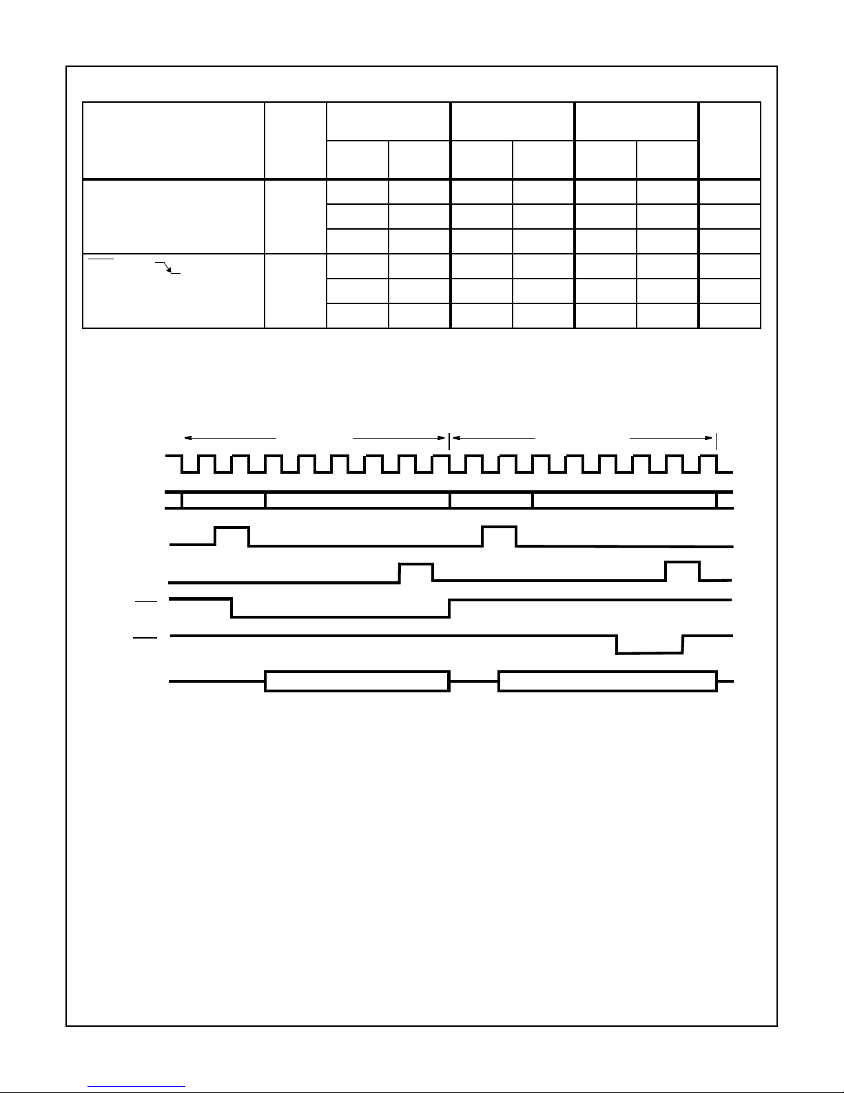
FIGURE 3. BASIC DC TIMING WAVEFORM, ONE INSTRUCTION CYCLE
FETCH (READ) EXECUTE (WRITE)
00 01 10 11 20 21 30 31 40 41 50 51 60 61 70 71 00 01 10 11 20 21 30 31 40 41 50 51 60 61 70 71 00
HI BYTE LOW BYTEHI BYTE LOW BYTE
CLOCK
ADDRESS
TPA
TPB
MRD
MWR
DATA VALID INPUT DATA VALID OUTPUT DATA
CDP1802A, CDP1802AC, CDP1802BC
Page 10
3-12
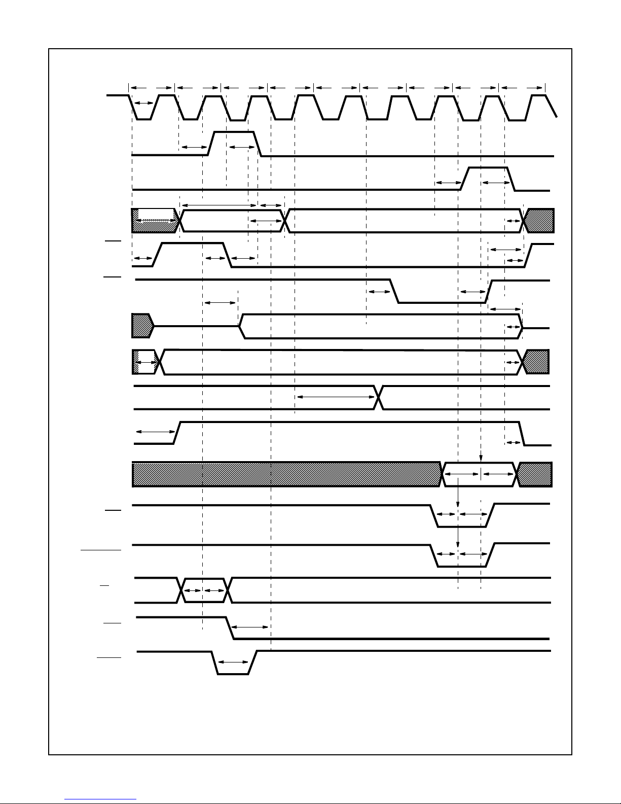
NOTES:
1. This timing diagram is used to show signal relationships only and does not represent any specific machine cycle.
2. All measurements are referenced to 50% point of the waveforms.
3. Shaded areas indicate “Don’t Care” or undefined state. Multiple transitions may occur during this period.
FIGURE 4. TIMING WAVEFORM
Timing Waveforms (Continued)
CLOCK
TPA
TPB
MEMORY
MRD
MWR
(I/O EXEC UTION
Q
DATA FROM
DMA
INTERRUPT
EF 1-4
WAIT
CLEAR
REQUEST
REQUEST
BUS TO CPU
N0, N1, N2
STATE
DATA FROM
CPU TO BUS
(MEMORY
WRITE CYCLE)
(MEMORY
ADDRESS
READ CYCLE)
CODES
CYCLE)
t
W
00 10 20 30 40 50 60 70 0001 11 21 31 41 51 61 71 01
0 1 2 3 4 5 6 7 0
t
PLH
t
PHL
t
PLH
t
PHL
t
PLH
, t
PHL
t
SU
DMA SAMPLED (S1, S2, S3)
t
H
ADDRESS BYTE
HIGH ORDER
t
PHL
t
PLH
t
SU
t
PLH
, t
PHL
t
PLH
, t
PHL
t
PLH
t
H
t
PLH
t
H
t
PLH
, t
PHL
t
PLH
, t
PHL
t
PLH
, t
PHL
ADDRESS BYTE
LOW ORDER
t
PHL
t
PLH
t
PHL
t
PLH
t
PHL
t
PLH
t
PLH
DATA
LATCHED IN CPU
t
SU
t
H
t
SU
t
H
t
SU
t
H
INTERRUPT
SAMPLED (S1, S2)
FLAG LINES
SAMPLED (IN S1)
ANY NEGATIVE
TRANSITION
t
SU
t
W
t
SUtH
CDP1802A, CDP1802AC, CDP1802BC
Page 11

3-13
Machine Cycle Timing Waveforms (Propagation Delays Not Shown)
FIGURE 5. GENERAL TIMING WAVEFORMS
FIGURE 6. NON-MEMORY CYCLE TIMING WAVEFORMS
FIGURE 7. MEMO RY WRITE CYCLE TIMING WAVEFORMS
CLOCK
TPA
TPB
MACHINE
MA
CYCLE
01 2345 6701 23456701 2345670
CYCLE n CYCLE (n + 1) CYCLE (n + 2)
LOW ADDRESSHIGH ADDLOW ADDRESSHIGH ADDLOW ADDRESSHIGH ADD
MEMORY READ CYCLENON MEMORY CYCLEMEMORY READ CYCLE
INSTRUCTION
MRD
MWR (HIGH)
MEMORY
OUTPUT
FETCH (S0) EXECUTE (S1) FETCH (S0)
EXECUTE
ALLOWABLE MEMORY ACCESS
VALID OUTPUT VALID
OUTPUT
“DON’T CARE” OR INTERNAL DELAYS
HIGH IMPEDANCE STATE
MEMORY
OUTPUT
ALLOWABLE MEMORY ACCESS
VALID OUTPUT VALID
OUTPUT
MEMORY READ CYCLEMEMORY WRITE CYCLEMEMORY READ CYCLE
INSTRUCTION FETCH (S0) EXECUTE (S1) FETCH (S0)
EXECUTE
CPU OUTPUT
OFF VALID DATA OFF
VALID
MWR
MRD
TO MEMORY
“DON’T CARE” OR INTERNAL DELAYS
HIGH IMPEDANCE STATE
CDP1802A, CDP1802AC, CDP1802BC
Page 12

3-14
FIGURE 8. MEMORY READ CYCLE TIMING WAVEFORMS
FIGURE 9. LONG BRANCH OR LONG SKIP CYCLE TIMING WAVEFORMS
Machine Cycle Timing Waveforms (Propagation Delays Not Shown) (Continued)
MEMORY READ CYCLEMEMORY READ CYCLEMEMORY READ CYCLE
INSTRUCTION FETCH (S0) EXECUTE (S1) FETCH (S0)
EXECUT
E
MEMORY
OUTPUT
ALLOWABLE MEMORY ACCESS
VALID OUTPUT
VALID
OUTPUT
MRD
MWR (HIGH)
“DON’T CARE” OR INTERNAL DELAYS
HIGH IMPEDANCE STATE
VALID
OUTPUT
MEMORY
OUTPUT
ALLOWABLE MEMORY ACCESS
VALID OUTPUT
VALID
OUTPUT
MEMORY READ CYCLEMEMORY READ CYCLEMEMORY READ CYCLE
INSTRUCTION FETCH (S0) EXECUTE (S1) EXECUTE (S1)
FETCH (S
0)
MRD
MWR (HIGH)
“DON’T CARE” OR INTERNAL DELAYS
HIGH IMPEDANCE STATE
VALID OUTPUT
CDP1802A, CDP1802AC, CDP1802BC
Page 13

3-15
FIGURE 10. INPUT CYCLE TIMING WAVEFORMS
FIGURE 11. OUTPUT CYCLE TIMING WAVEFORMS
Machine Cycle Timing Waveforms (Propagation Delays Not Shown) (Continued)
CLOCK
0123
456701234567
MEMORY
OUTPUT
ALLOWABLE MEMORY ACCESS
VALID OUTPUT
TPA
TPB
MACHINE
INSTRUCTION
MRD
N0 - N2
DATA
MWR
CYCLE
BUS
MEMORY READ CYCLE MEMORY WRITE CYCLE
VALID DATA FROM INPUT DEVICE
N = 9 - F
EXECUTE (S1)
CYCLE ( n + 1)CYCLE n
FETCH (S0)
NOTE 1
“DON’T CARE” OR INTERNAL DELAYS
HIGH IMPEDANCE STATE
(NOTE 1)
USER GENERATED SIGNAL
0
CLOCK
0123
456701234567
TPA
TPB
MACHINE
INSTRUCTION
CYCLE
EXECUTE (S1)
CYCLE (n + 1)CYCLE n
FETCH (S0)
DATA BUS
ALLOWABLE MEMORY ACCESS
VA LID OUTPUT
VALID DATA FROM MEMORY
ALLOWABLE MEMORY ACCESS
MEMORY READ CYCLEMEMORY READ CYCLE
MRD
N0 - N2
DATA STROBE
(MRD
• TPB • N)
NOTE 1
“DON’T CARE” OR INTERNAL DELAYS
HIGH IMPEDANCE STATE
(NOTE 1)
USER GENERATED SIGNAL
0
N = 1 - 9
CDP1802A, CDP1802AC, CDP1802BC
Page 14

3-16
FIGURE 12. DMA IN CYCLE TIMING WAVEFORMS
FIGURE 13. DMA OUT
CYCLE TIMING WAVEFORMS
Machine Cycle Timing Waveforms (Propagation Delays Not Shown) (Continued)
CLOCK
0123
45670123456701 23
TPA
TPB
MACHINE
I
NSTRUCTION
DMA-IN
MRD
MWR
MEMORY
DATA BUS
CYCLE
OUTPUT
4567
NOTE 1
MEMORY READ CYCLE MEMORY READ, WRITE MEMORY WRITE CYCLE
OR NON-MEMORY CYCLE
“DON’T CARE” OR INTERNAL DELAYS
HIGH IMPEDANCE STATE
(NOTE 1)
USER GENERATED SIGNAL
VALID DATA FROM INPUT DEVICE
CYCLE n
FETCH (S0)
CYCLE (n+1)
EXECUTE (S1)
CYCLE (n+2)
DMA (S2)
VA LID OUTPUT
01234567012345670123456
CLOCK
TPA
TPB
MACHINE
CYCLE
INSTRUCTION
DMA OUT
MRD
MWR
MEMORY
OUTPUT
DATA
STROBE
(S2 • TPB)
CYCLE n CYCLE (n + 1) CYCLE (n + 2)
DMA (S2)EXECUTE (S1)FETCH (S0)
VALID OUTPUT VALID DATA FROM MEMORY
NOTE 1
MEMORY READ CYCLE MEMORY READ, WRITE MEMORY READ CYCLE
OR NON-MEMORY CYCLE
“DON’T CARE” OR INTERNAL DELAYS
HIGH IMPEDANCE STATE
USER GENERATED SIGNAL
(NOTE 1)
(NOTE 1)
CDP1802A, CDP1802AC, CDP1802BC
Page 15

3-17
FIGURE 14. INTERRUPT CYCLE TIMING WAVEFORMS
Performance Curves
FIGURE 15. CDP1802A, AC TYPICAL MA XIMUM CLOCK
FREQUENCY AS A FUNCTION OF TEMPERATURE
FIGURE 16. CDP1802BC TYPICAL MAXIMUM CLOCK
FREQUENCY AS A FUNCTION OF TEMPERATURE
Machine Cycle Timing Waveforms (Propagation Delays Not Shown) (Continued)
01234567012345670123456
CLOCK
TPA
TPB
MACHINE
CYCLE
INSTRUCTION
CYCLE n CYCLE (n + 1) CYCLE (n + 2)
INTERRUPT (S3)EXECUTE (S1)FETCH (S0)
MRD
MWR
INTERRUPT
MEMORY
OUTPUT
VA LID OUTPUT
NOTE 1
MEMORY READ CYCLE
MEMORY READ, WRITE
NON-MEMORY CYCLE
OR NON-MEMORY CYCLE
“DON’T CARE” OR INTERNAL DELAYS
HIGH IMPEDANCE STATE
(NOTE 1)
(
INTERNAL) IE
USER GENERATED SIGNAL
8
7
6
5
4
3
2
1
0
25 35 45 55 65 75 85 95 105 115 125
f
CL
, SYSTEM MAXIMUM CLOCK
FREQUENCY (MHz)
TA, AMBIENT TEMPERATURE (oC)
CL, LOAD CAPACITANCE = 50pF
VCC = VDD = 10V
VCC = 5V, VDD = 10V
VCC = VDD = 5V
CL, LOAD CAPACITANCE = 50pF
VCC = VDD = 5V
8
7
6
5
4
3
2
1
0
25 35 45 55 65 75 85 95 105 115 125
f
CL
, SYSTEM MAXIMUM CLOCK
FREQUENCY (MHz)
TA, AMBIENT TEMPERATURE (oC)
CDP1802A, CDP1802AC, CDP1802BC
Page 16

3-18
FIGURE 17. TYPICAL TRANSITION TIME vs LOAD CAPACI-
TANCE FOR ALL TYPES
FIGURE 18. CDP1802A, AC MINIMUM OUTPUT HIGH (SOURCE)
CURRENT CHARACTERISTICS
FIGURE 19. CDP1802A, AC MINIMUM OUTPUT LOW (SINK)
CURRENT CHARACTERISTICS
FIGURE 20. CDP1802BC MINIMUM OUTPUT HIGH (SOURCE)
CURRENT CHARACTERISTICS
Performance Curves (Continued)
400
350
300
250
200
150
100
50
0
0 25 50 75 100 125 150 175 200
t
THL,
t
TLH
, TRANSITION TIME (ns)
CL, LOAD CAPACITANCE (pF)
TA = 25oC
VCC = VDD = 10V
VCC = VDD = 5V
VCC = VDD = 5V
VCC = VDD = 10V
t
TLH
t
THL
VGS, GATE-TO-VOL TAGE = -5V
TA, AMBIENT TEMPERATURE = -40oC TO +85oC
-10V
V
DS
, DRAIN-TO-SOURCE VOLTAGE (V)
-10-9 -8-7-6 -5-4-3-2-10
1
2
3
4
5
6
7
I
OH
, OUTPUT HIGH (SOURCE) CURRENT (mA)
VGS, GATE-TO-SOURCE = 10V
TA = -40oC TO +85oC
5V
V
DS
, DRAIN-TO-SOURCE VOLTAGE (V)
I
OL
, OUTPUT LOW (SINK) CURRENT (mA)
012345678910
5
10
15
20
25
30
35
VGS, GA T E-TO-VOLTAGE = -5V
V
DS
, DRAIN-TO-SOURCE VOLTAGE (V)
-5 -4 -3 -2 -1 0
1
2
3
4
I
OH
, OUTPUT HIGH (SOURCE) CURRENT (mA)
CDP1802A, CDP1802AC, CDP1802BC
Page 17

3-19
Signal Descriptions
Bus 0 to Bus 7 (Data Bus)
8-bit bidirectional DATA BUS lines. These lines are used for
transferring data between the memory, the microprocessor,
and I/O devices.
N0 to N2 (I/O Control Lines)
Activated by an I/O instruction to signal the I/O control logic of
a data transfer between memory and I/O interface. These
lines can be used to issue command codes or device selection codes to the I/O devices (independently or combined with
the memory byte on the data bus when an I/O instruction is
being executed). The N bits are low at all times except when
an I/O instruction is being executed. During this time their
state is the same as the corresponding bit s in the N reg ister.
The direction of data flow is defined in the I/O instruction b y bit
N3 (internally) and is indicated by the level of the MRD signal.
MRD
= VCC: Data from I/O to CPU and Memory
MRD
= VSS: Data from Memory to I/O
EF1
to EF4 (4 Flags)
These inputs enable the I/O controllers to transfer status
information to the processor. The levels can be tested by the
conditional branch instructions. They can be used in conjunction with the INTERRUPT request line to establish interrupt priorities. These flags can also be used by I/O devices
to “call the attention” of the process or, in which case the program must routinely test the status of these flag(s). The
flag(s) are sampled at the beginning of every S1 cycle.
FIGURE 21. CDP1802BC MINIMUM OUTP UT LOW (SINK)
CURRENT CHARACTERISTICS
FIGURE 22. TYPICAL CHANGE IN PROPAGA TION DELAY AS A
FUNCTION OF A CHANGE IN LOAD CAPACIT ANCE
FOR ALL TYPES
NOTE: IDLE = “00” AT M(0000), BRANCH = “3707” AT M(8107), CL = 50pF
FIGURE 23. TYPICAL POWER DISSIPATION AS A FUNCTION OF CLOCK FREQUENCY FOR BRANCH INSTRUCTION AND IDLE
INSTRUCTION FOR ALL TYPES
Performance Curves (Continued)
VGS, GATE-TO-SOURCE = 5V
TA = -40oC TO +85oC
V
DS
, DRAIN-TO-SOURCE VOLTAGE (V)
I
OL
, OUTPUT LOW (SINK) CURRENT (mA)
012345
5
10
20
150
125
100
75
50
25
0
25 50 100 150 200
∆t
PLH
, ∆t
PHL
, ∆ PROPAGATION DELAY
TIME (ns)
∆CL, ∆ LOAD CAPACITANCE (pF)
TA = 25oC
VCC = VDD = 10V
VCC = VDD = 5V
VCC = VDD = 5V
VCC = VDD = 10V
∆t
PLH
∆t
PHL
NOTE: ANY OUTPUT EXCEPT XTAL
TA = 25oC
P
D
, TYPICAL POWER DISSIPATION
FOR CDP1802D (mW)
fCL, CLOCK INPUT FREQUENCY (MHz)
0.01 0.1 1 10
0.1
1
10
100
1000
VCC = VDD = 10V
BRANCH
IDLE
VCC = VDD = 5V
CDP1802A, CDP1802AC, CDP1802BC
Page 18

3-20
INTERRUPT, DMA-lN, DMA-OUT (3 I/O Requests)
These inputs are sampled by the CPU during the interval
between the leading edge of TPB and the leading edge of
TPA.
Interrupt Action - X and P are stored in T after executing
current instruction; designator X is set to 2; designator P is
set to 1; interrupt enable is reset to 0 (inhibit); and instruction
execution is resumed. The interrupt action requires one
machine cycle ( S3).
DMA Action - Finish executing current instruction; R(0)
points to memory area for data transfer; data is loaded into
or read out of memory; and increment R(0).
NOTE: In the event of concurrent DMA an d Inter rupt re que sts,
DMA-lN has priority followed b y D M A-OUT a nd th en Inte rrupt.
SC0, SC1, (2 State Code Lines)
These outputs indicate that the CPU is: 1) fetching an
instruction, or 2) executing an instruction, or 3) processing a
DMA request, or 4) acknowledging an interrupt request. The
levels of state code are tabulated below. All states are valid
at TPA. H = V
CC
, L = VSS.
TPA, TPB (2 Timing Pulses)
Positive pulses that occur once in each machine cycle (TPB
follows TPA). They are used by I/O controller s to interpret
codes and to time interaction with the data bus. The trailing
edge of TPA is used by the memory system to latch the
higher-order byte of the 16-bit memory address. TPA is suppressed in IDLE when the CPU is in the load mode.
MA0 to MA7 (8 Memory Address Lines)
In each cycle, the higher-order byte of a 16-bit CPU memory
address appears on the memory address lines MA0-7 first.
Those bits required by the memory system can be strobed
into external address latches by timing pulse TPA. The low
order byte of the 16-bit address appears on the address lines
after the termination of TPA. Latching of all 8 higher-order
address bits would permit a memory system of 64K bytes .
MWR
(Write Pulse)
A negative pulse appearing in a memory-write cycle, after
the address lines have stabilized.
MRD
(Read Level)
A low level on MRD indicates a memory read cycle. It can be
used to control three-state outputs from the addressed memory which may have a common data input and output bus. If a
memory does not have a three-state high-impedance output,
MRD is useful for driving memory/bus separator gates. It is
also used to indicate the direction of data transfer during an
I/O instruction. For additional information see Table 1.
Q
Single bit output from the CPU which can be set or reset
under program control. During SEQ or REQ instruction execution, Q is set or reset betwee n the traili ng edge of TPA and
the leading edge of TPB.
CLOCK
Input for externally generated single-phase clock. The clock is
counted down internally to 8 clock pulses per machine cyc le.
XTAL
Connection to be u sed w it h c lock in put terminal, for an external crystal, if the on-chip oscillator is utilized. The crystal is
connected between terminals 1 and 39 (CLOCK and XTAL)
in parallel with a resistance (10MΩ typ). Frequency trimming
capacitors may be required at terminals 1 and 39. For additional information, see Applic ati on No te AN656 5.
WAIT
, CLEAR (2 Control Lines)
Provide four control modes as listed in the following truth table:
VDD, VSS, VCC (Power Levels)
The internal voltage supply VDD is isolated from the
Input/Output voltage supply V
CC
so that the processor may
operate at maximum speed while interfacing with peripheral
devices operating at lower voltage. V
CC
must be less than or
equal to V
DD
. All outputs swing from VSS to VCC. The recom-
mended input voltage swing is V
SS
to VCC.
Architecture
The CPU block diagram is shown in Figure 2. The principal
feature of this syste m i s a regi st er array (R) consisting of sixteen 16-bit scratchpad registers. Individual registers in the
array (R) are designated (selected) by a 4-bit binary code
from one of the 4-bit registers labeled N, P and X. The contents of any registe r can be dir ected to any one of the following three paths:
1. The e xterna l m em ory (m ulti pl exe d, hig her-o rde r byte first,
on to 8 memory address lines).
2. The D re gis ter (eith er o f the two b yt es c an be gat ed to D ).
3. The increment/decrement circuit where it is increased or
decreased by one and stored back in the selected 16-bit
register.
STATE TYPE
STATE CODE LINES
SC1 SC0
S0 (Fetch) L L
S1 (Execute) L H
S2 (DMA) H L
S3 (Interrupt) H H
CLEAR WAIT MODE
LLLOAD
LHRESET
HLPAUSE
H H RUN
CDP1802A, CDP1802AC, CDP1802BC
Page 19

3-21
The three pat hs, depen ding on the natu re of the in stru ction,
may operate independently or in various combinations in the
same machine cycle.
With two exceptions, CPU instruction consists of two 8clock-pulse machine cycles. The first cycle is the fetch cycle,
and the second - and third if necessary - are execute cycles.
During the fetch cycle the four bits in the P designator select
one of the 16 registers R(P) as the current program counter.
The selected regist er R( P) co nt a ins the a ddress of the memory location from which the instruction is to be fetched. When
the instruction is read out from the memory, the higher order
4 bits of the instruction byte are loaded into the register and
the lower order 4 bits into the N register. The content of the
program counter is a uto ma tic all y i nc rem ented by one so that
R(P) is now “pointing” to the next byte in the memory.
The X designator selects one of the 16 registers R(X) to
“point” to the memory fo r an o pera nd (or d at a ) i n cert a in ALU
or I/O operations.
The N designator can perform the following five functions
depending on the type of instruct ion fetche d:
1. Designate one of the 16 registers in R to be acted upon
during register operations.
2. Indicate to the I/O devices a command code or device
selection code for peripherals.
3. Indicate the specific operation to be executed during the
ALU instructions, types of test to be performed during the
Branch instruction, or the specific operation required in a
class of miscellaneous instructions (70 - 73 and 78 - 7B).
4. Indicate the value to be loaded into P to designate a new
register to be used as the program counter R(P).
5. Indicate the value to be loaded into X to designate a new
register to be used as data pointer R(X).
The registers in R can be assigned by a programmer in three
different ways: as program counters, as data pointers, or as
scratchpad locations (data registers) to hold two bytes of dat a.
Program Counters
Any register can be the main program counter; the address
of the selected regi ster is held in the P desi gnator. Other registers in R can be used as subroutine program counters. By
single instruction the contents of the P register can be
changed to effect a “call” to a subroutine. When interrupts
are being serviced, register R(1) is used as the program
counter for the user's interrupt servic ing routine. After reset,
and during a DMA operation, R(0) is used as the program
counter. At all other times the register designated as program counter is at the discretion of the user.
Data Pointers
The registers in R may be us ed as dat a poi nters to i ndica te a
location in memory. The register designated by X (i.e., R(X))
points to memory for the following instructions (see Table 1).
1. ALU operations F1 - F5, F7, 74, 75, 77
2. Output in structions 61 through 67
3. Input instructions 69 through 6F
4. Certain miscellaneous instructions - 70 - 73, 78, 60, F0
The register designated by N (i.e., R(N)) points to memory
for the “load D from me mo ry” ins truc ti ons 0N a nd 4N an d th e
“Store D” instruction 5N. The register designated by P (i.e.,
the program counter) is used as the data pointer for ALU
instructions F8 - FD, FF, 7C, 7D, 7F. During these instruction
executions, the operation is referred to as “data immediate”.
Another important use of R as a data pointer supports the
built-in Direct-Memory-Access (DMA) function. When a
DMA-ln or DMA-Out request is received, one machine cycle
is “stolen”. This operation occurs at the end of the execute
machine cycle in the current instruction. Register R(0) is
always used as the data pointer during the DMA operation.
The data is read from (DM A-O ut) o r w ritte n i nto (DMA-l n) th e
memory location pointed to by the R(0) register. At the end
of the trans fer, R(0) is increment ed by one so that the processor is ready to act upon the next DMA byte transfer
request. This feature in the 1800-series architecture saves a
substantial amo unt of logic when fast exch anges of blo cks of
data are required, such as with magnetic discs or during
CRT-display-refresh cycles.
Data Registers
When registers in R are used to store bytes of data, four
instructions are provided which allow D to receive from or
write into either the higher-order or lower-order byte portions
of the register de si gna ted by N. By this mechanism (together
with loading by data immediate) program pointer and data
pointer designations are initialized. Also, this technique
allows scratchpad registers in R to be used to hold general
data. By employing increment or decrement instructions,
such registers may be used as loop counters.
The Q Flip-Flop
An internal flip-flop, Q, can be set or reset by instruction and
can be sensed by co nditio nal bra nch in structi ons. T he outp ut
of Q is also available as a microprocessor output.
CDP1802A, CDP1802AC, CDP1802BC
Page 20
3-22
Interrupt Servicing
Register R(1) is always used as the program counter whenever interrupt servicing is initiated. When an interrupt
request occurs and the interrupt is allowed by the program
(again, nothing takes place until the completion of the current instruction), the contents of the X and P registers are
stored in the temporary register T, and X and P are set to
new values; hex digit 2 in X and hex digit 1 in P. Interrupt
Enable is automatically deactivated to inhibit further interrupts. The user's interrupt routine is now in control; the contents of T may b e save d by m eans o f a sin gle ins tructi on (7 8)
in the memory location pointed to by R(X). At the conclusion
of the interrupt, the user's routine may restore the pre-interrupted value of X and P with a single instruction (70 or 71).
The Interrupt Enable flip-flop can be activated to permit further interrupts or can be disabled to prevent them.
CPU Register Summary
CDP1802 Control Modes
The WAIT
and CLEAR lines provide four control modes as
listed in the following truth t ab le:
The function of the modes are defined as follows:
Load
Holds the CPU in the I D LE ex ec uti on s t a te and allows an I/O
device to load the memory with out the need for a “bootstrap”
loader. It modifies the IDLE condition so that DMA-lN operation does not force execution of the next inst ruc tio n.
Reset
Registers l, N, Q are reset, lE is set and 0’s (VSS) are placed on
the data bus. TPA and TPB are suppressed while reset is held
and the CPU is placed in S1. The f irst machine cycle after termination of reset is an initialization cycle which requires 9 clock
pulses. During this cycle the CPU remains in S1 and register X,
P, and R(0) are reset. Interrupt and DMA servicing are sup-
pressed during the initialization cycle. The ne xt cycle is an S0,
S1, or an S2 but never an S3. Wit h the u se of a 7 1 instruction
followed by 00 at memory locations 0000 and 0001, this feature
may be used to reset IE, so as to preclude interrupts until ready
for them. Power-up reset can be realized by connecting an RC
network directly to the CLEAR pin, since it has a Schmitt triggered input, see Figure 24.
Pause
Stops the internal CPU timing generator on the first negative
high-to-low transitio n of the input clock. The oscillator continues to operate, but s ubs eq uen t cl oc k tra ns iti ons are ign ore d.
Run
May be initiated from the Pause or Reset mode functions. If
initiated from Pause, the CPU resumes operation on the first
negative high-to-low transition of the input clock. When initiated from the Rese t o peration, the first machine cycle foll owing Reset is a lways the initia lization cycl e. The initiali zation
cycle is then follow e d by a DMA (S2) cycle or fetch (S0) from
location 0000 in memory.
Run-Mode State Transitions
The CPU state transitions when in the RUN and RESET
modes are shown in Fi gure 25. Each machine cycle requires
the same period of time, 8 clock pulses, except the initialization cycle, which requires 9 clock pulses. The execution of
an instruction requires either two or three machine cycles,
S0 followed by a single S1 cycle or two S1 cycles. S2 is the
response to a DMA request an d S3 is the interru pt respo nse.
Table 2 shows the conditions on Data Bus and Memory
Address lines during all machine states.
Instruction Set
The CPU instruction summar y is given in Table 1. Hexadecimal notation is used to refer to the 4-bit binary codes.
In all registers bit s are num bered f rom the l east s ignifi cant b it
(LSB) to the most significant bit (MSB) starting with 0.
R(W): Register designated by W, where
W = N or X, or P
R(W).0: Lower order byte of R(W)
R(W).1: Higher order byte of R(W)
Operation Notation
M(R(N)) → D; R(N) + 1 → R(N)
This notation means: The memory byte pointed to by R(N) is
D 8 Bits Data Register (Accumulator)
DF 1-Bit Data Flag (ALU Carry)
B 8 Bits Auxiliary Holding Register
R 16 Bits 1 of 16 Scratchpad Registers
P 4 Bits Designates which register is Program Counter
X 4 Bits Designates which register is Data Pointer
N 4 Bits Holds Low-Order Instruction Digit
I 4 Bits Holds High-Order Instruction Digit
T 8 Bits Holds old X, P after Interrupt (X is high nibble)
lE 1-Bit Interrupt Enable
Q 1-Bit Output Flip-Flop
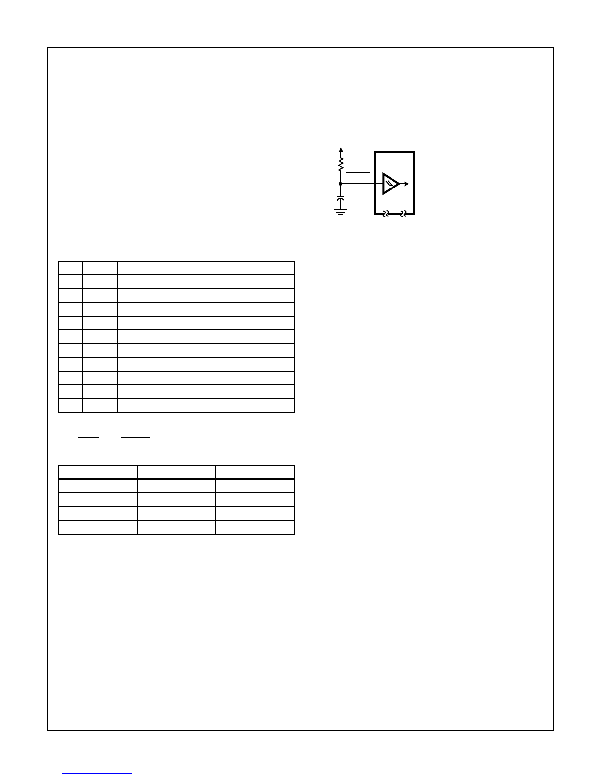
CLEAR
WAIT MODE
LLLOAD
L H RESET
H L PAUSE
H H RUN
CLEAR
V
CC
R
S
C
CDP1802
3
THE RC TIME CONSTANT
SHOULD BE GREATER THAN
THE OSCILLATOR START-UP
TIME (TYPICALLY 20ms)
FIGURE 24. RESET DIAGRAM
CDP1802A, CDP1802AC, CDP1802BC
Page 21

3-23
loaded into D, and R(N) is incremented by 1.
FIGURE 25. STATE TRANSITION DIAGRAM
T ABLE 1. INSTRUCTION SUMMARY (SEE NOTES)
INSTRUCTION MNEMONICOPCODE OPERATION
MEMORY REFERENCE
LOAD VIA N LDN 0N M(R(N)) → D; FOR N not 0
LOAD ADVANCE LDA 4N M(R(N)) → D; R(N) + 1 → R(N)
LOAD VIA X LDX F0 M( R(X)) → D
LOAD VIA X AND ADVANCE LDXA 72 M(R (X)) → D; R(X) + 1 → R(X)
LOAD IMMEDIATE LDl F8 M(R(P)) → D; R(P) + 1 → R(P)
STORE VIA N STR 5N D → M(R(N))
STORE VIA X AND DECREMENT STXD 73 D → M(R(X)); R(X) - 1 → R(X)
REGISTER OPERATIONS
INCREMENT REG N INC 1N R(N) + 1 → R(N)
DECREMENT REG N DEC 2N R(N) - 1 → R(N)
INCREMENT REG X IRX 60 R(X) + 1 → R(X)
GET LOW REG N GLO 8N R(N).0 → D
PUT LOW REG N PLO AN D → R(N).0
GET HIGH REG N GHl 9N R(N).1 → D
PUT HIGH REG N PHI BN D → R(N).1
LOGIC OPERATIONS (Note 1)
OR OR F1 M(R(X)) OR D → D
OR IMMEDIATE ORl F9 M(R(P)) OR D → D; R(P) + 1 → R(P)
S2 DMA
S1 RESET
S1 EXECUTE
S0 FETCH
S3 INT
S1 INIT
DMA DMA
DMA
• INT
DMA
DMA
IDLE • DMA
• INT
FORCE S1
(LONG BRANCH,
DMA
• IDLE • INT
DMA
DMA
INT • DMA
LONG SKIP, NOP, ETC.)
PRIORITY: FORCE S0, S1
DMA
IN
DMA
OUT
INT
INT • DMA
CDP1802A, CDP1802AC, CDP1802BC
Page 22

3-24
EXCLUSIVE OR XOR F3 M(R(X)) XOR D → D
EXCLUSIVE OR IMMEDIATE XRI FB M(R(P)) XOR D → D; R(P) + 1 → R(P)
AND AND F2 M(R(X)) AND D → D
AND IMMEDIATE ANl FA M(R(P)) AND D → D; R(P) + 1 → R(P)
SHIFT RIGHT SHR F6 SHIFT D RIGHT, LSB(D) → DF, 0 → MSB(D)
SHIFT RIGHT WITH CARRY SHRC 76
(Note 2)
SHIFT D RIGHT, LSB(D) → DF, DF → MSB(D)
RING SHIFT RIGHT RSHR 76
(Note 2)
SHIFT D RIGHT, LSB(D) → DF, DF → MSB(D)
SHIFT LEFT SHL FE SHIFT D LEFT, M SB(D) → DF, 0 → LSB(D)
SHIFT LEFT WITH CARRY SHLC 7E
(Note 2)
SHIFT D LEFT, MSB(D) → DF, DF → LSB(D)
RING SHIFT LEFT RSHL 7E
(Note 2)
SHIFT D LEFT, MSB(D) → DF, DF → LSB(D)
ARITHMETIC OPERATIONS (Note 1)
ADD ADD F4 M(R(X)) + D → DF, D
ADD IMMEDIATE ADl FC M(R(P)) + D → DF, D; R(P) + 1 → R(P)
ADD WITH CARRY ADC 74 M(R(X)) + D + DF → DF, D
ADD WITH CARRY, IMMEDIATE ADCl 7C M(R(P)) + D + DF → DF, D; R(P) + 1 → R(P)
SUBTRACT D SD F5 M(R(X)) - D → DF, D
SUBTRACT D IMMEDIATE SDl FD M(R(P)) - D → DF, D; R(P) + 1 → R(P)
SUBTRACT D WITH BORROW SDB 75 M(R(X)) - D - (NOT DF) → DF, D
SUBTRACT D WITH BORROW, IMMEDIATE SDBl 7D M( R(P)) - D - (Not DF) → DF, D; R(P) + 1 → R(P)
SUBTRACT MEMORY SM F7 D-M(R(X)) → DF, D
SUBTRACT MEMORY IMMEDIATE SMl FF D-M(R(P)) → DF, D; R(P) + 1 → R(P)
SUBTRACT MEMORY WITH BORROW SM B 77 D-M(R(X ))-(NO T DF) → DF, D
SUBTRACT MEMORY WITH BORROW, IMMEDI-
ATE
SMBl 7F D-M(R(P))-(NOT DF) → DF, D; R(P) + 1 → R(P)
BRANCH INSTRUCTIONS - SHORT BRANCH
SHORT BRANCH BR 30 M(R(P)) → R(P).0
NO SHORT BRANCH (See SKP) NBR 38
(Note 2)
R(P) + 1 → R(P)
SHORT BRANCH IF D = 0 BZ 32 IF D = 0, M(R(P)) → R(P).0, ELSE R (P) + 1 → R(P)
SHORT BRANCH IF D NOT 0 BNZ 3A IF D NOT 0, M(R(P)) → R(P).0, ELSE R(P) + 1 → R(P)
SHORT BRANCH IF DF = 1 BDF 33
(Note 2)
IF DF = 1, M(R(P)) → R(P).0, ELSE R(P) + 1 → R(P)
SHORT BRANCH IF POS OR ZERO BPZ
SHORT BRANCH IF EQUAL OR GREATER BGE
SHORT BRANCH IF DF = 0 BNF 3B
(Note 2)
IF DF = 0, M(R(P)) → R(P).0, ELSE R(P) + 1 → R(P)
SHORT BRANCH IF MINUS BM
SHORT BRANCH IF LESS BL
SHORT BRANCH IF Q = 1 BQ 31 IF Q = 1, M(R(P)) → R( P).0, ELSE R(P) + 1 → R(P)
SHORT BRANCH IF Q = 0 BNQ 39 IF Q = 0, M(R(P)) → R(P).0, ELSE R(P) + 1 → R(P)
TABLE 1. INSTRUCTION SUMMARY (SEE NOTES) (Continued)
INSTRUCTION MNEMONICOPCODE OPERATION
CDP1802A, CDP1802AC, CDP1802BC
Page 23

3-25
SHORT BRANCH IF EF1 = 1 (EF1 = VSS) B1 34 IF EF1 =1, M(R(P)) → R(P).0, ELSE R (P) + 1 → R(P)
SHORT BRANCH IF EF1 = 0 (EF1
= VCC) BN1 3C IF EF1 = 0, M(R(P)) → R(P).0, ELSE R(P) + 1 → R(P)
SHORT BRANCH IF EF2 = 1 (EF2
= VSS) B2 35 IF EF2 = 1, M(R(P)) → R(P).0, ELSE R(P) + 1 → R(P)
SHORT BRANCH IF EF2 = 0 (EF2 = VCC) BN2 3D IF EF2 = 0, M(R(P)) → R(P).0, ELSE R(P) + 1 → R(P)
SHORT BRANCH IF EF3 = 1 (EF3
= VSS) B3 36 IF EF3 = 1, M(R(P)) → R(P).0, ELSE R(P) + 1 → R(P)
SHORT BRANCH IF EF3 = 0 (EF3
= VCC) BN3 3E IF EF3 = 0, M(R(P)) → R(P).0, ELSE R(P) + 1 → R(P)
SHORT BRANCH IF EF4 = 1 (EF4
= VSS) B4 37 IF EF4 = 1, M(R(P)) → R(P).0, ELSE R(P) + 1 → R(P)
SHORT BRANCH IF EF4 = 0 (EF4 = VCC) BN4 3F IF EF4 = 0, M(R(P)) → R(P).0, ELSE R(P) + 1 → R(P)
BRANCH INSTRUCTIONS - LONG BRANCH
LONG BRANCH LBR C0 M(R(P)) → R(P). 1, M(R(P) + 1) → R(P).0
NO LONG BRANCH (See LSKP) NLBR C8
(Note 2)
R(P) = 2 → R(P)
LONG BRANCH IF D = 0 LBZ C2 lF D = 0, M(R(P)) → R(P).1, M(R(P) +1) → R(P).0,
ELSE R(P) + 2 → R(P)
LONG BRANCH IF D NOT 0 LBNZ CA IF D Not 0, M(R(P)) → R(P).1, M(R(P) + 1) → R(P).0, ELSE
R(P) + 2 → R(P)
LONG BRANCH IF DF = 1 LBDF C3 lF DF = 1, M(R(P)) → R(P).1, M(R(P) + 1) → R(P).0, ELSE
R(P) + 2 → R(P)
LONG BRANCH IF DF = 0 LBNF CB IF DF = 0, M(R(P)) → R(P).1, M(R(P) + 1) → R(P).0, ELSE
R(P) + 2 → R(P)
LONG BRANCH IF Q = 1 LBQ C1 IF Q = 1, M(R(P)) → R(P).1, M(R(P) + 1) → R(P).0,
ELSE R(P) + 2 → R(P)
LONG BRANCH lF Q = 0 LBNQ C9 lF Q = 0, M(R(P)) → R(P).1, M(R(P) + 1) → R(P).0
EISE R(P) + 2 → R(P)
SKIP INSTRUCTIONS
SHORT SKIP (See NBR) SKP 38
(Note 2)
R(P) + 1 → R(P)
LONG SKIP (See NLBR) LSKP C8
(Note 2)
R(P) + 2 → R(P)
LONG SKIP IF D = 0 LSZ CE IF D = 0, R(P) + 2 → R(P), ELSE CONTINUE
LONG SKIP IF D NOT 0 LSNZ C6 IF D Not 0, R(P) + 2 → R(P), ELSE CONTINUE
LONG SKIP IF DF = 1 LSDF C F IF DF = 1, R(P) + 2 → R(P), ELSE CONTINUE
LONG SKIP IF DF = 0 LSNF C7 IF DF = 0, R(P) + 2 → R(P), ELSE CONTINUE
LONG SKIP lF Q = 1 LSQ CD IF Q = 1, R ( P) + 2 → R(P), ELSE CONTINUE
LONG SKIP IF Q = 0 LSNQ C5 IF Q = 0, R(P) + 2 → R(P), ELSE CONTINUE
LONG SKIP IF lE = 1 LSlE CC IF IE = 1, R(P) + 2 → R(P), ELSE CONTINUE
CONTROL INSTRUCTIONS
IDLE lDL 00
(Note 3)
WAIT FOR DMA OR INTERRUPT; M(R(0)) → BUS
NO OPERATION NOP C4 CONTINUE
SET P SEP DN N → P
SET X SEX EN N → X
SET Q SEQ 7B 1 → Q
TABLE 1. INSTRUCTION SUMMARY (SEE NOTES) (Continued)
INSTRUCTION MNEMONICOPCODE OPERATION
CDP1802A, CDP1802AC, CDP1802BC
Page 24

3-26
RESET Q REQ 7A 0 → Q
SAVE SAV 78 T → M(R(X))
PUSH X, P TO STACK MARK 79 (X, P) → T; (X, P) → M(R(2)), THEN P → X; R(2) - 1 → R(2)
RETURN RET 70 M(R(X)) → (X, P); R(X) + 1 → R(X), 1 → lE
DISABLE DlS 71 M(R(X)) → (X, P); R(X) + 1 → R(X), 0 → lE
INPUT - OUTPUT BYTE TRANSFER
OUTPUT 1 OUT 1 61 M(R(X)) → BUS; R (X) + 1 → R(X); N LINES = 1
OUTPUT 2 OUT 2 62 M(R(X)) → BUS; R (X) + 1 → R(X); N LINES = 2
OUTPUT 3 OUT 3 63 M(R(X)) → BUS; R (X) + 1 → R(X); N LINES = 3
OUTPUT 4 OUT 4 64 M(R(X)) → BUS; R (X) + 1 → R(X); N LINES = 4
OUTPUT 5 OUT 5 65 M(R(X)) → BUS; R (X) + 1 → R(X); N LINES = 5
OUTPUT 6 OUT 6 66 M(R(X)) → BUS; R (X) + 1 → R(X); N LINES = 6
OUTPUT 7 OUT 7 67 M(R(X)) → BUS; R (X) + 1 → R(X); N LINES = 7
INPUT 1 INP 1 69 BUS → M(R(X)); BUS → D; N LINES = 1
INPUT 2 INP 2 6A BUS → M(R(X)); BUS → D; N LINES = 2
INPUT 3 INP 3 6B BUS → M(R(X)); BUS → D; N LINES = 3
INPUT 4 INP 4 6C BUS → M(R(X)); BUS → D; N LINES = 4
INPUT 5 INP 5 6D BUS → M(R(X)); BUS → D; N LINES = 5
INPUT 6 INP 6 6E BUS → M(R(X)); BUS → D; N LINES = 6
INPUT 7 INP 7 6F BUS → M(R(X)); BUS → D; N LINES = 7
TABLE 1. INSTRUCTION SUMMARY (SEE NOTES) (Continued)
INSTRUCTION MNEMONICOPCODE OPERATION
CDP1802A, CDP1802AC, CDP1802BC
Page 25

3-27
NOTES: (For Table 1)
1. The arithmetic operations and the shift instructions are the only instructions that can alter the DF.
After an add instruction:
DF = 1 denotes a carry has occurred
DF = 0 Denotes a carry has not occurred
After a subtract instruction:
DF = 1 denotes no borrow. D is a true positive number
DF = 0 denotes a borrow. D is two’s complement
The syntax “-(not DF)” denotes the subtraction of the borrow.
2. This instruction is associated with more than one mnemonic. Each mnemonic is individually listed.
3. An idle instruction initiates a repeating S1 cycle. The processor will continue to idle until an I/O request (INTERRUPT
, DMA-lN, or DMA- OUT) is
activated. When the request is acknowledged, the idle cycle is terminated and the I/O request is serviced, and then normal operation is resumed.
4. Long-Branch, Long-Skip and No Op instructions require three cycles to complete (1 fetch + 2 execute).
Long-Branch instructions are three bytes long. The first byte specifies the condition to be te sted; and the second and third byte, the
branching address.
The long-branch instructions can:
a. Branch unconditionally
b. Test for D = 0 or D ≠ 0
c. Test for DF = 0 or DF = 1
d. Test for Q = 0 or Q = 1
e. Effect an unconditional no branch
If the tested condition is met, then branching takes place; the branching address bytes are loaded in the high-and-low order bytes of the
current program counter, respectively. This operation effects a branch to any memory location.
If the tested condition is not met, the branching address bytes are skipped over, and the next instruction in sequence is fetched and executed. This operation is taken for the case of unconditional no branch (NLBR).
5. The short-branch instructions are two bytes long. The first byte specifies the condition to be tested, and the second specifies the branching address.
The short branch instruction can:
a. Branch unconditionally
b. Test for D = 0 or D ≠ 0
c. Test for DF = 0 or DF = 1
d. Test for Q = 0 or Q = 1
e. Test the status (1 or 0) of the four EF flags
f. Effect an unconditional no branch
If the tested condition is met, then branching takes place; the branching address byte is loaded into the low-order byte position of the
current program counter. This effects a branch within the current 256-byte page of the memory, i.e., the page which holds the branching
address. If the tested condition is not met, the branching address byte is skipped over, and the next instruction in sequence is fetched
and executed. This same action is taken in the case of unconditional no branch (NBR).
6. The skip instructions are one byte long. There is one Unconditional Short-Skip (SKP) and eight Long-Skip instructions.
The Unconditional Short-Skip instruction takes 2 cycles to complete (1 fetch + 1 execute). Its action is to skip over the byte following it.
Then the next instruction in sequence is fetched and executed. This SKP instruction is identical to the unconditional no-branch instruction (NBR) except that the skipped-over byte is not considered part of the program.
The Long-Skip instructions take three cycles to complete (1 fetch + 2 execute).
They can:
a. Skip unconditionally
b. Test for D = 0 or D ≠ 0
c. Test for DF = 0 or DF = 1
d. Test for Q = 0 or Q = 1
e. Test fo r IE = 1
If the tested condition is met, then Long Skip takes place; the current program counter is incremented twice. Thus two bytes are skipped
over, and the next instruction in sequence is fetched and executed. If the tested condition is not met, then no action is taken. Execution
is continued by fetching the next instruction in sequence.
TABLE 1. INSTRUCTION SUMMARY (SEE NOTES) (Continued)
INSTRUCTION MNEMONICOPCODE OPERATION
CDP1802A, CDP1802AC, CDP1802BC
Page 26

3-28
T ABLE 2. CONDITIONS ON DA TA BUS AND MEMORY ADDRESS LINES DURING ALL MACHINE STATES
STATE I N SYMBOL OPERATION
DATA
BUS
MEMORY
ADDRESS MRD
MWR
N
LINES NOTES
S1 RESET 0 → I, N, Q, X, P; 1 → lE 00 XXXX 1 1 0 1
Initialize, Not Programmer
Accessible
0000 → R00XXXX1102
S0 FETCH MRP → l, N; RP + 1 → RP MRP RP 0 1 0 3
S1 0 0 lDL IDLE MR0 RO 0 1 0 4, Fig. 8
01 - F LDN MRN → D MRN RN 0 1 0 Fig. 8
1 0 - F INC RN + 1 → RN Float RN 1 1 0 Fig. 6
2 0 - F DEC RN - 1 → RN Float RN 1 1 0 Fig. 6
3 0 - F Short Branch Taken: MRP → RP.0
Not Taken; RP + 1 → RP
MRP RP 0 1 0 Fig. 8
40 - F LDA MRN → D; RN + 1 → RN MRN RN 0 1 0 Fig. 8
50 - F STR D → MRN D RN 1 0 0 Fig. 7
60 IRX RX + 1 → RX MRX RX 0 1 0 Fig. 7
61 OUT 1MRX → BUS; RX + 1 → RX MRX RX 0 1 1 Fig. 11
2OUT 2 2Fig. 11
3OUT 3 3Fig. 11
4OUT 4 4Fig. 11
5OUT 5 5Fig. 11
6OUT 6 6Fig. 11
7OUT 7 7Fig. 11
9 INP 1 BUS → MRX, D Data from
I/O Device
RX 1 0 1 Fig. 10
AINP 2 2Fig. 10
BINP 3 3Fig. 10
CINP 4 4Fig. 10
DINP5 5Fig. 10
EINP6 6Fig. 10
FINP7 7Fig. 10
7 0 RET MRX → (X, P); RX + 1 → RX;
1 → lE
MRX RX 0 1 0 Fig. 8
1 DlS MRX → (X, P); RX + 1 → RX;
0 → lE
MRX RX 0 1 0 Fig. 8
2 LDXA MRX → D; RX + 1 → RX MRX RX 0 1 0 Fig. 8
3STXDD → MRX; RX - 1 → RX D RX 1 0 0 Fig. 7
4 ADC MRX + D + DF → DF, D MRX RX 0 1 0 Fig. 8
5 SDB MRX - D - DFN → DF, D MRX RX 0 1 0 Fig. 8
6 SHRC LSB(D) → DF; DF → MSB(D) Float RX 1 1 0 Fig. 6
7 SMB D - MRX - DFN → DF, D MRX RX 0 1 0 Fig. 8
8SAVT → MRX T RX 1 0 0 Fig. 7
CDP1802A, CDP1802AC, CDP1802BC
Page 27

3-29
S1 7 9 MARK (X, P) → T, MR2; P → X;
R2 - 1 → R2
TR2100Fig. 7
AREQ0 → Q Float RP 1 1 0 Fig. 6
BSEQ1 → Q Float RP 1 1 0 Fig. 6
C ADCl MRP + D + DF → DF, D;
RP + 1
MRP RP 0 1 0 Fig. 8
D SDBl MRP - D - DFN → DF, D;
RP + 1
MRP RP 0 1 0 Fig. 8
E SH LC MSB(D) → DF; DF → LSB(D) Float RP 1 1 0 Fig. 6
F SMBl D - MRP - DFN → DF, D;
RP + 1
MRP RP 0 1 0 Fig. 8
8 0 - F GLO RN.0 → D RN.0 RN 1 1 0 Fig. 6
9 0 - F GHl RN.1 → D RN.1 RN 1 1 0 Fig. 6
A0 - F PLO D → RN.0 D RN 1 1 0 Fig. 6
B0 - F PHI D → RN.1 D RN 1 1 0 Fig. 6
S1#1 C 0 - 3,
8 - B
Long Branch Taken: MRP → B; RP + 1 → RPMRP RP 0 1 0 Fig. 9
#2 Taken: B → RP.1;
MRP → RP.0
M(RP + 1) RP + 1 0 1 0 Fig. 9
S1#1 Not Taken: RP + 1 → RP MRP RP 0 1 0 Fig. 9
#2 Not Taken: RP + 1 → RP M(RP + 1) RP + 1 0 1 0 Fig. 9
S1#1 5
6
7
C
D
E
F
Long Skip Taken: RP + 1 → RP MRP RP 0 1 0 Fig. 9
#2 Taken: RP + 1 → RP M(RP + 1) RP + 1 0 1 0 Fig. 9
S1#1 Not Taken: No Operation MRP RP 0 1 0 Fig. 9
#2 Not Taken: No Operation MRP RP 0 1 0 Fig. 9
S1#1 4 NOP No Operation MRP RP 0 1 0 Fig. 9
#2 No Operation MRP RP 0 1 0 Fig. 9
S1 D 0 - F SEP N → PNNRN110Fig. 6
E0 - F SEX N → XNNRN110Fig. 6
S1 F 0 LDX MRX → D MRX RX 0 1 0 Fig. 8
1
2
3
4
5
7
OR
AND
XOR
ADD
SD
SM
MRX OR D → D
MRX AND D → D
MRX XOR D → D
MRX + D → DF, D
MRX - D → DF, D
D - MRX → DF, D
MRX RX 0 1 0 Fig. 8
6SHRLSB(D) → DF; 0 → MSB(D) Float RX 1 1 0 Fig. 6
TABLE 2. CONDITIONS ON DATA BUS AND MEMORY ADDRESS LINES DURING ALL MACHINE STATES (Continued)
STATE I N SYMBOL OPERATION
DATA
BUS
MEMORY
ADDRESS MRD
MWR
N
LINES NOTES
CDP1802A, CDP1802AC, CDP1802BC
Page 28

3-30
All Intersil U.S. products are manufa ct ured , asse mbled and tested utilizing ISO9000 quality systems.
Intersil Corporation’s quality certifications can be viewed at www.intersil.com/design/quality
Intersil products are sold by description only. Intersil Corporation reserves the right to make changes in circuit design, software and/or specifications at any time wit hout
notice. Accordingly, the reader is cautioned to verify that data sheets are current before placing orders. Information furnished by Intersil is believed to be accurate and
reliable. However, no responsibility is assumed by Intersil or its subsidi aries for it s use; nor for any infri ngemen t s of pat ent s or other rights of third parties which may result
from its use. No license is granted by implication or otherwise under any patent or patent rights of Intersil or its subsidiaries.
For information regarding Intersil Corporation and its products, see www.intersil.com
Operating and Handling Considerations
Handling
All inputs and out puts of Inter sil CMOS devic es have a network for electrostatic protection during handling.
Operating
Operating Voltage - During operation near the maximum
supply voltage limit care should be taken to avoid or suppress
power supply turn-on and turn-off transient s, pow er supply ripple, or ground noise; any of these conditions must not cause
V
DD
- VSS to exceed the absolute maximum rating.
Input Signals - To prevent damage to the input protection
circuit, input signals should never be greater than V
DD
nor
less than V
SS
. Input currents must not exceed 10mA ev en
when the power supply is off.
Unused Inputs - A connection must be provided at every
input terminal. All unuse d inp ut term in als must be co nne cted
to either V
DD
or VSS, whichever is appropriate.
Output Sh ort Circu its - Shorting of out puts to V
DD
or V
SS
may damage CMOS devices by exceeding the maximum
device dissipation.
S1 F 8 LDl MRP → D; RP + 1 → RP MRP RP 0 1 0 Fig. 8
9ORlMRP OR D → D; RP + 1 → RP
A ANl MRP AND D → D; RP + 1 → RP
B XRl MRP XOR D → D; RP + 1 →
RP
CADlMRP + D → DF , D; RP + 1 →
RP
D SDl MRP - D → DF, D; RP + 1 →
RP
F SMl D - MRP → DF, D; RP +1 →
RP
ESHLMSB(D) → DF; 0 → LSB(D) Float RP 1 1 0 Fig. 6
S2 DMA IN BUS → MR0; R0 + 1 → R0 Data from
I/O Device
R0 1 0 0 6, Fig. 12
DMAOUT MR0 → BUS; R0 + 1 → R0 MR0 R0 0 1 0 6, Fig. 13
S3 INTERRUPT X, P → T; 0 → lE, 1 → P;
2 → X
Float RN 1 1 0 Fig. 14
S1 LOAD IDLE (CLEAR
, WAlT = 0) M(R0 - 1) R0 - 1 0 1 0 5, Fig. 8
NOTES:
1. lE = 1, TPA, TPB suppressed, state = S1.
2. BUS = 0 for entire cycle.
3. Next state always S1.
4. Wait for DMA or INTERRUPT.
5. Suppress TPA, wait for DMA.
6. IN REQUEST has priority over OUT REQUEST .
7. See Timing Waveforms, Figure 5 through Figure 14 for machine cycles.
TABLE 2. CONDITIONS ON DATA BUS AND MEMORY ADDRESS LINES DURING ALL MACHINE STATES (Continued)
STATE I N SYMBOL OPERATION
DATA
BUS
MEMORY
ADDRESS MRD
MWR
N
LINES NOTES
 Loading...