Intersil Corporation CDP1020 Datasheet
CDP1020
Data Sheet April 1999
SMBus/I2C ACPI Dual Device Bay
Controller
The CDP1020 is an ACPI compliant Device Bay Controller
(DBC) that can control two device bays. The controller
interfaces to the host system through the industry standard
2
I
C or System Management Bus (SMBus) and is fully
compliant with Device BaySpecification0.90.TheCDP1020
is designed to be compatible with the integratedSMBushost
controller of the PiiX4/PiiX6 in Intel Architecture platforms.
The CDP1020 is designed to be placed on the host
motherboard, on a riser, or adjacent to the Device Bay
connectors. The required clock source is generated from an
internal oscillator on the CLK pin, with an external RC to set
the frequency. This lowers the system cost and allows the
CDP1020 to remain active during S3-S5 system states
where all clock generators have been stopped.
One of the key features of this device is the on-chip level
shifters that provide slew rate controlled, direct gate drive for
external N-Channel MOSFETs (Intersil HUF76113DK8
recommended) to switch the device bay V
Switching an N-Channel device as opposed to a P-Channel
reduces both device cost and device count, resulting in an
overall lower system cost.
Configuration data for the CDP1020, including subsystem
vendor ID, subsystem revision, bay size and device bay
capabilities are designed to be written into the CDP1020 by
the system BIOS at power up. The registers for this data are
write-once-only and thus become read-only after the initial
BIOS write.
supplies.
ID
File Number
4704
Features
• Fully Compliant with Device Bay Specification 0.90 and
ACPI Specification 1.0
• Industry Standard SMBus/I
2
C Interface
• Controls for Two Device Bays
• Onboard Level Shifting for Direct Drive of N-Channel
MOSFET VID Switches
• Integrated Pull-up Resistors on 1394PRx, USBPRx,
SECUREx, and REMREQx Inputs
• RC Type Oscillator - Low Cost and Low Power
Consumption
• Operational Voltage from 3.3 to 5.5V
• “5V Tolerant” Inputs at all Operating Voltages
• Write-Once BIOS/External Configuration
• Removal Request Input for Each Bay
• Security Lock Input for Each Bay
• High Current Device Bay LED Indicator Drivers With
Separate High-Side Power Input
• Configurable Level/Pulse Bay Solenoid Drivers
• Programmable Insertion Time Out Delay
• HCMOS Technology; 28 Lead Plastic SOIC
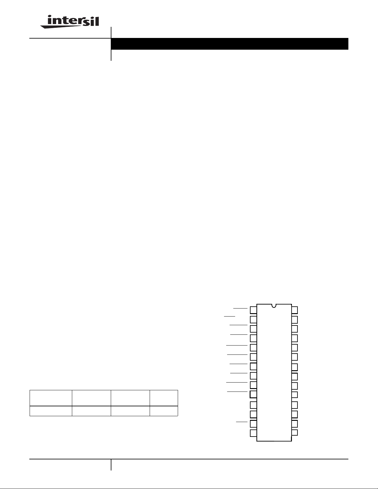
Pinout
CDP1020 (SOIC)
TOP VIEW
The address selection pins (AD1 and AD0) allow the
CDP1020 to occupy any one of four I
2
C/SMBus addresses.
This enables up to four CDP1020 devices to coexist in a
system.
The CDP1020 implements high current outputs for direct
drive (with a limiting resistor) of the optional bay status
LEDs. These indicators are two color (green/amber)
common anode or anti-parallel LEDs that indicate the device
bay status per the Device Bay Specification 0.90.
Ordering Information
PART
NUMBER
CDP1020 0 to 85 28 Ld SOIC M28.3
For More Information Contact:
Mike Coletta (714) 433-0600
Terry Pierce (407) 729-5835
TEMP. RANGE
(oC) PACKAGE PKG. NO.
2-418
CAUTION: These devices are sensitive to electrostatic discharge; follow proper IC Handling Procedures.
SDA
SCK
ALRT
GATE
1
2
3
4
5
6
7
8
9
10
11
12
13
14
RESET
TEST (VDD)
1394PR0
USBPR0
REMREQ0
SECURE0
1394PR1
USBPR1
REMREQ1
SECURE1
http://www.intersil.com or 407-727-9207
28
AD1
27
AD0
26
CLK
25
V
SS
24
V
DD
23
V
LED
22
LEDA1
21
LEDG1
LEDA0
20
19
LEDG0
18
SFTLOCK1
SFTLOCK0
17
16
PWREN1
15
PWREN0V
| Copyright © Intersil Corporation 1999
CDP1020
Pin Descriptions
PIN NUMBER PIN NAME IN/OUT PIN DESCRIPTION
1
2
3 1394PR0 IN Bay 0 1394 Presence Input with Active Pull-up
4
5
6
7
8
9
10
11 SDA IN/OUT SMBus/I
12 SCK IN/OUT SMBus/I
13
14 V
15 PWREN0 OUT Bay 0 Power Enable 12V NMOS Gate Drive Output
16 PWREN1 OUT Bay 1 Power Enable 12V NMOS Gate Drive Output
17 SFTLOCK0 OUT Bay 0 Software Controlled Lock Mechanism Driver
18 SFTLOCK1 OUT Bay 1 Software Controlled Lock Mechanism Driver
19 LEDG0 OUT Bay 0 Status Indicator (Green LED) Driver
20 LEDA0 OUT Bay 0 Status Indicator (Amber LED) Driver
21 LEDG1 OUT Bay 1 Status Indicator (Green LED) Driver
22 LEDA1 OUT Bay 1 Status Indicator (Amber LED) Driver
23 V
24 V
25 V
26 CLK IN External Clock Schmitt Input (for RC oscillator)
27 AD0 IN SMBus/I
28 AD1 IN SMBus/I
RESET IN Device Bay Controller Master Reset Schmitt Input
TEST - Test pin used by manufacturer only. Must be externally connected to V
USBPR0 IN Bay 0 USB Presence Input with Active Pull-up
REMREQ0 IN Bay 0 Remove Request Input with Active Pull-up
SECURE0 IN Bay 0 Security Input with Active Pull-up
1394PR1 IN Bay 1 1394 Presence Input with Active Pull-up
USBPR1 IN Bay 1 USB Presence Input with Active Pull-up
REMREQ1 IN Bay 1 Remove Request Input with Active Pull-up
SECURE1 IN Bay 1 Security Input with Active Pull-up
2
C Data Schmitt Input/Open-Drain Output
2
C Clock Schmitt Input/Open-Drain Output
ALRT OUT SMBus Alert Open-Drain Output
GATE
LED
DD
SS
- Power Supply Input for PWREN0/PWREN1 Drivers
- Power Supply Input for LED Driver (LEDAx, LEDGx)
- Power Supply Input (Power)
- Power Supply Return (Ground or GND)
2
C Address Configuration Bit 0
2
C Address Configuration Bit 1
DD
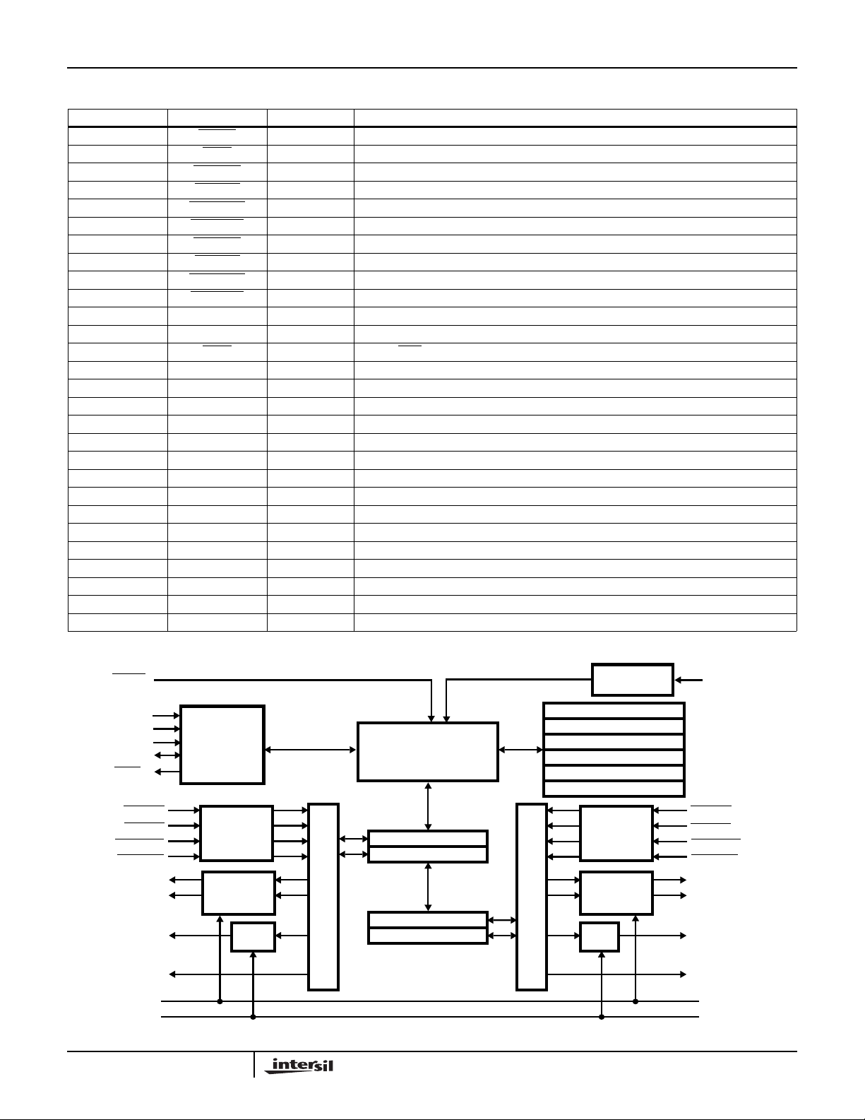
Block Diagram
RESET CLK
AD1
AD0
SCK
SDA
ALRT
1394PR0
USBPR0
REMREQ0
SECURE0
LEDA0
LEDG0
PWREN0
SFTLOCK0
V
LED
V
GATE
I2C/SMBus
INTERFACE
DEBOUNCE
LOGIC and
PULLUP Rs
TIMER/
LEVEL
SHIFTER
LEVEL
SHIFT
DEVICE BAY 0 CONTROLLER
DEVICE BAY
CONTROLLER LOGIC
BSTR0 - $10
BCER0 - $14
BSTR1 - $18
BCER1 - $1C
OSCILLATOR
CIRCUITRY
VENDOR - $00
REVISION - $04
SUBSYS VENDOR - $08
SUBSYS REV- $0A
DBCCR - $0C
SFR - $FC
DEBOUNCE
LOGIC and
PULLUP Rs
TIMER/
LEVEL
SHIFTER
LEVEL
SHIFT
DEVICE BAY 1 CONTROLLER
1394PR1
USBPR1
REMREQ1
SECURE1
LEDA1
LEDG1
PWREN1
SFTLOCK1
V
LED
V
GATE
2-419
CDP1020
Absolute Maximum Ratings Thermal Information
Supply Voltage, VDD . . . . . . . . . . . . . . . . . . . . . . . . . . -0.5V to +6V
Supply Voltage, V
Supply Voltage, V
. . . . . . . . . . . . . . . . . . . . . . . . . VDD to 13V
GATE
. . . . . . . . . . . . . . . . . . . . . . . . . -0.5V to +6V
LED
Input Voltage, VIN . . . . . . . . . . . . . . . . . . VSS - 0.3V to VDD + 0.3V
Test Mode, VIN . . . . . . . . . . . . . . . . . . . . VSS - 0.3V to 2 x VDD + 0.3V
Current Drain Per Pin Excluding VDD and VSS, I . . . . . . . . . . 40mA
Operating Conditions
Voltage Range. . . . . . . . . . . . . . . . . . . . . . . . . . . . . +3.0V to +5.0V
Temperature Range. . . . . . . . . . . . . . . . . . . . . . . . . . . 0oC to 85oC
Input High Voltage . . . . . . . . . . . . . . . . . . . . . . . (0.8 x VDD) to V
CAUTION: Stresses above those listed in “Absolute Maximum Ratings” may cause permanent damage to the device. This is a stress only rating and operationofthe
device at these or any other conditions above those indicated in the operational sections of this specification is not implied.
NOTE:
1. θJA is measured with the component mounted on an evaluation PC board in free air.
DD
Thermal Resistance (Typical, Note 1) θJA (oC/W)
28 Ld SOIC . . . . . . . . . . . . . . . . . . . . . . . . . . . . . . . 60
Maximum Junction Temperature . . . . . . . . . . . . . . . . . . . . . . .150oC
Maximum Storage Temperature Range (T
). . . . -65oC to 150oC
STG
Maximum Lead Temperature (Soldering 10s) . . . . . . . . . . . . .300oC
(SOIC - Lead Tips Only)
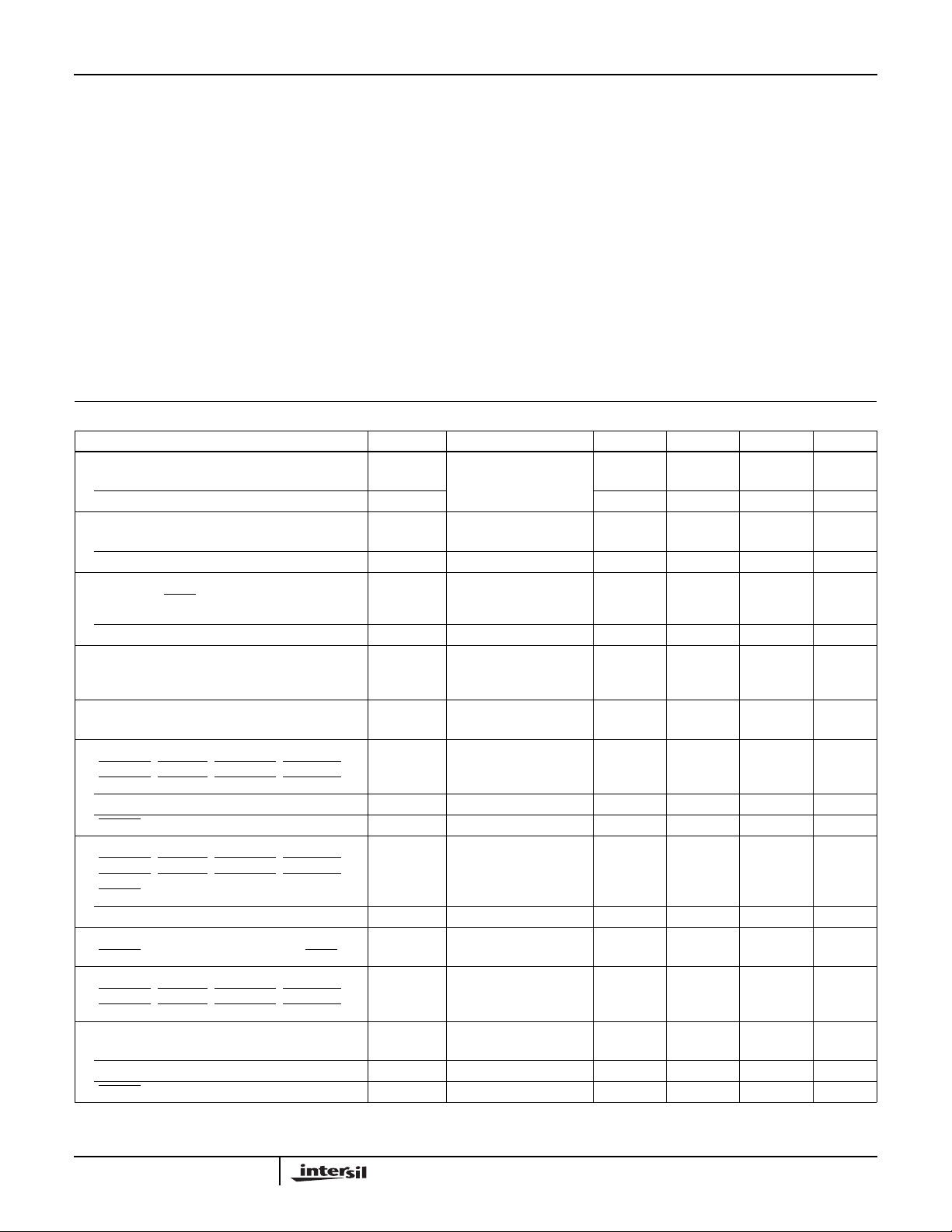
DC Electrical Specifications, 5.0V V
= 5.0V ±10%, TA = 0oC to 85oC
DD
PARAMETER SYMBOL CONDITIONS MIN TYP MAX UNITS
Output Voltage -10µA < I
All Outputs V
SFTLOCK0, SFTLOCK1 V
OL
OH
Output High Voltage
LEDA0, LEDG0, LEDA1, LEDG1 V
SFTLOCK0, SFTLOCK1 V
OH
OH
I
LOAD
I
LOAD
Output Low Voltage
SCK, SDA,
ALRT, SFTLOCK0, SFTLOCK1,
V
OL
I
LOAD
LEDG0, LEDA0, LEDG1, LEDA1
PWREN0, PWREN1 V
OL
I
LOAD
Gate Output High Voltage
PWREN0, PWREN1 V
GOH
I
LOAD
Gate Output Current Source
PWREN0, PWREN1 I
GATE
Input High Voltage
1394PR0, USBPR0, REMREQ0, SECURE0,
V
IH
1394PR1, USBPR1, REMREQ1, SECURE1
SCK, SDA V
RESET, CLK V
IH
IH
Input Low Voltage
1394PR0, USBPR0, REMREQ0, SECURE0,
V
IL
1394PR1, USBPR1, REMREQ1, SECURE1,
RESET, CLK
SCK, SDA V
IL
Input/Output Leakage Current:
RESET, CLK, AD0, AD1, SCK, SDA, ALRTI
IOL
Input Pullup Current
1394PR0, USBPR0, REMREQ0, SECURE0,
I
IN
1394PR1, USBPR1, REMREQ1, SECURE1
Input Hysteresis Voltage
SCK, SDA V
CLK V
RESET V
HYS
HYS
HYS
< 10µA
LOAD
- - 0.1 V
VDD - 0.1 - - V
= -16.0mA V
- 1.0 - - V
LED
= -0.7mA VDD - 0.3 - - V
= 1.6mA - - 0.4 V
= 60µA - - 0.4 V
< 10µAV
GATE
-0.5V
V
GATE
-0.3V
V
GATE
-15 -35 -50 µA
0.7•V
0.7•V
0.7•V
V
V
DD
DD
DD
SS
SS
-VDDV
-VDDV
-VDDV
- 0.2•V
- 0.2•V
DD
DD
--±10 µA
50 200 400 µA
0.02 0.10 0.40 V
0.6 1.0 1.3 V
0.8 1.1 1.4 V
V
V
V
2-420
CDP1020
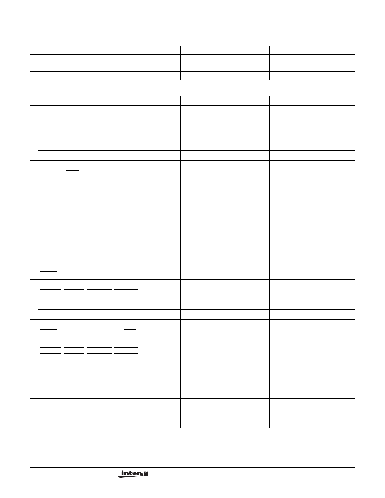
DC Electrical Specifications, 5.0V V
= 5.0V ±10%, TA = 0oC to 85oC (Continued)
DD
PARAMETER SYMBOL CONDITIONS MIN TYP MAX UNITS
Capacitance C
Supply Current (RUN) I
DC Electrical Specifications, 3.3V V
DD
OUT
C
IN
f
DD
= 4.0MHz External - 1.3 5.0 mA
CLK
= 3.3V ±10%, TA = 0oC to 85oC
PARAMETER SYMBOL CONDITIONS MIN TYP MAX UNITS
Output Voltage -10µA < I
All Outputs V
SFTLOCK0, SFTLOCK1 V
OL
OH
Output High Voltage
LEDA0, LEDG0, LEDA1, LEDG1 V
SFTLOCK0, SFTLOCK1 V
OH
OH
I
LOAD
I
LOAD
Output Low Voltage
SCK, SDA,
ALRT, SFTLOCK0, SFTLOCK1,
V
OL
I
LOAD
LEDG0, LEDA0, LEDG1, LEDA1
PWREN0, PWREN1 V
OL
I
LOAD
Gate Output High Voltage
PWREN0, PWREN1 V
GOH
I
LOAD
Gate Output Current Source
PWREN0, PWREN1 I
GATE
Input High Voltage
1394PR0, USBPR0, REMREQ0, SECURE0,
V
IH
1394PR1, USBPR1, REMREQ1, SECURE1
SCK, SDA V
RESET, CLK V
IH
IH
Input Low Voltage
1394PR0, USBPR0, REMREQ0, SECURE0,
V
IL
1394PR1, USBPR1, REMREQ1, SECURE1,
RESET, CLK
SCK, SDA V
IL
Input/Output Leakage Current:
RESET, CLK, AD0, AD1, SCK, SDA, ALRTI
IOL
Input Pullup Current
1394PR0, USBPR0, REMREQ0, SECURE0,
I
IN
1394PR1, USBPR1, REMREQ1, SECURE1
Input Hysteresis Voltage
SCK, SDA V
CLK V
RESET V
Capacitance C
Supply Current (RUN) I
HYS
HYS
HYS
OUT
C
DD
IN
- - 12 pF
--8pF
< 10µA
LOAD
- - 0.1 V
VDD - 0.1 - - V
= -6.0mA V
- 1.0 - - V
LED
= -0.4mA VDD - 0.3 - - V
= 1.6mA - - 0.4 V
= 50µA - - 0.4 V
< 10µAV
GATE
-0.5V
V
GATE
-0.3V
V
GATE
-10 -20 -30 µA
0.7•V
0.7•V
0.7•V
V
V
DD
DD
DD
SS
SS
-VDDV
-VDDV
-VDDV
- 0.2•V
- 0.2•V
DD
DD
--±10 µA
20 80 160 µA
0.05 0.15 0.45 V
0.4 0.8 1.1 V
0.3 0.5 0.8 V
- - 12 pF
--8pF
- 0.9 4.5 mA
V
V
V
2-421
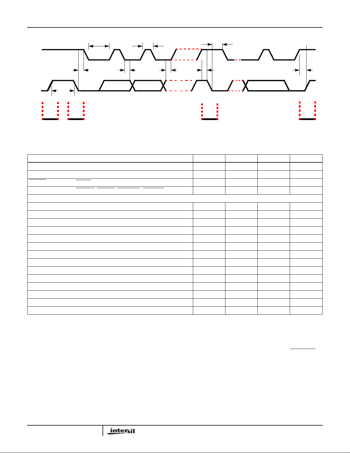
CDP1020
t
LOW
SCK
t
HD:STA
SDA
t
BUF
STOP START START
t
HD:DAT
t
HIGH
t
SU:DAT
STOP
t
SU:STA
t
HD:STA
FIGURE 1. CONTROL TIMING
Control Timing V
= 3.3V ±10%, TA = 0oC to 85oC
DD
PARAMETER SYMBOL MIN MAX UNITS
Frequency Of Operation (4.0MHz nominal) (CLK Pin) f
Suspend Recovery Start-up Time t
RESET Pulse Width (RESET Pin) t
Input Debounce Time (1394PRx, USBPRx, REMREQx, SECUREx Pins) t
CLK
RSUS
RL
DB
2.0 4.5 MHz
0.9 1 ms
6-t
50 - ms
SMBus SCK and SDA Pins
SCK Frequency f
SMBus Free Time t
Hold Time After (Repeated) Start Condition t
Repeated Start Condition Setup Time t
Stop Condition Setup Time t
Data Hold Time t
Data Setup Time t
SCK Time-out Period t
HD:STA
SU:STA
SU:STO
HD:DAT
SU:DAT
TIMEOUT
SCK Low Period t
SCK High Period t
Slave SCK Extend Period (cumulative) t
Master SCK Extend Period (cumulative) t
LOW:SEXT
LOW:MEXT
SCK/SMBDAT Fall Time t
SCK/SMBDAT Rise Time t
SMB
BUF
LOW
HIGH
F
R
10 100 kHz
4.7 - µs
4.0 - µs
4.7 - µs
4.0 - µs
300 - ns
250 - ns
25 35 ms
4.7 - µs
4.0 50 µs
-25ms
-10ms
- 300 ns
- 1000 ns
t
SU:STO
OSC
Notational Conventions
The following conventions are used throughout this
document:
• Hexadecimal numbers are denoted with a “$” symbol
preceding the number.
• Binary numbers are represented with a “%” symbol
proceeding the number, or a “b” following.
• Because of the large mix of active-low and active-high
signals used in connection with the CDP1020, the terms
“asserted” and “de-asserted” will be used exclusively. An
active low signal is asserted when it is at a logic 0 and deasserted when it is at a logic 1 state. Conversely,an active
high signal is at a logic 1 state when asserted and at a
logic 0 state when de-asserted. The terms reset, clear,
2-422
and “low” can also mean logic 0; set or “high” can also
mean logic 1.
• Active low signals are represented with an overline; active
high signals have no overline. For example,
REMREQ0 is
active low, PWREN0 is active high.
• There are many pins, signals, registers, and software bits
common to both Bay 0 and Bay 1; these names may
include the Bay number suffix (0 or 1), an “x” to represent
either,or no suffix at all. For example, PWREN, PWREN0,
or PWRENx may each be used to describe output pin(s).
CDP1020
Functional Pin Descriptions
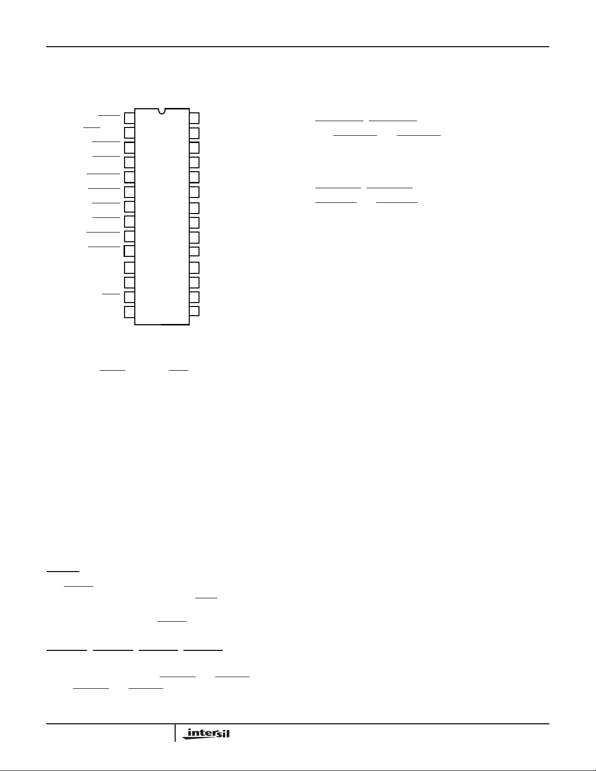
This section provides a description of each of the 28 pins of
the CDP1020 as shown in Figure 2.
SDA
SCK
ALRT
GATE
, V
1
2
3
4
5
6
7
8
9
10
11
12
13
14
, and VSS (Power Supply)
LED
RESET
TEST (VDD)
1394PR0
USBPR0
REMREQ0
SECURE0
1394PR1
USBPR1
REMREQ1
SECURE1
FIGURE 2. PINOUT DIAGRAM FOR THE CDP1020
NOTE: The following pins are “5V Tolerant” Inputs at all Operating
Voltages:CLK, RESET, SCK, SDA, ALRT. This means that the input
voltages can range up to the maximum allowed (5V typical),
regardless of the operating voltage of the IC.
VDD, V
GATE
Power is supplied to the CDP1020 using these pins. VDDis
connected to the positive logic supply (typically either 3.3V
or 5V), V
is connected to the positive supply for the
GATE
PWREN0 and PWREN1 gate drivers (typically 12V), V
connected to the positive power supply for the LED drivers
(typically 5V), and V
is connected to the negative supply
SS
(Ground).
NOTE: V
to the CDP1020 without the presence of the VDDand VSSsupplies.
Applying power to these inputs without the presence of the main
power supply could result in a condition where all level-shifted
outputs (PWRENx, LEDGx and LEDAx) track their power supply
input voltage, thus enabling any of their output circuitry.
GATE
and V
powersupplies should neverbe connected
LED
RESET (Reset Input)
The RESET input is a low level active input, which resets the
CDP1020. Resetting the device forces
the device to reset the state of each bay (see
Reset
for more details). The RESET pin contains an internal
Schmitt Trigger to improve noise immunity.
1394PR0, 1394PR1, USBPR0, USBPR1
These four pins are the device presence inputs to the device
bay controller for both bay 0 (
bay 1 (
1394PR1 and USBPR1). If the (peripheral) device
uses the 1394 or USB (or both), that pin(s) on its connector
1394PR0 and USBPR0) and
28
AD1
27
AD0
26
CLK
25
V
SS
24
V
DD
23
V
LED
22
LEDA1
21
LEDG1
LEDA0
20
19
LEDG0
18
SFTLOCK1
SFTLOCK0
17
16
PWREN1
15
PWREN0V
LED
ALRThigh and forces
Effects Of
is tied to GND (active low); when a device is inserted or
removed, these pins are monitored to reflect whether a
device is present (or not), and which of the two busses it
uses. All of these pins are CMOS inputs with internal active
pull-ups to V
DD
.
REMREQ0, REMREQ1
The REMREQ0 and REMREQ1 inputs are driven from the
“REMOVE REQUEST” buttons for bay 0 and bay 1,
respectively. These pins are CMOS inputs, with internal
active pull-ups to V
DD
.
SECURE0, SECURE1
SECURE0 and SECURE1 are inputs which are integral to
the bay security feature; each input should be connected
such that it will be asserted when an optional hardware lock
is engaged for the related bay. The state of these inputs are
observable by the operating system through the SL_STS
bits in the bay status registers. Both of these pins are CMOS
inputs with internal active pull-ups to V
DD
.
SDA (I2C/SMBus Data Input/Output)
The SDA pin is the serial data input to the SMBus interface
logic of the CDP1020; it contains an internal Schmitt Trigger
to improve noise immunity. When in slave-transmit mode,
this pin is an open drain output. Input thresholds for the SDA
input are fully compliant with SMBus Specification 1.0 (see
Electrical Specifications). Refer to the
Interface
text for more details.
I2C/SMBus
SCK (I2C/SMBus Clock Input)
The SCK pin is the serial clock input to the SMBus interface
logic of the CDP1020; it contains an internal Schmitt Trigger
to improve noise immunity. Since the CDP1020 never acts
as a SMBus master, this pin is a dedicated clock input
is
(except for clock-stretching protocol, where it uses an opendrain low-sideoutput). Input thresholds for the SCK input are
fully compliant with SMBus Specification 1.0 (see Electrical
Specifications). Refer to the
I2C/SMBus Interface
text for
more details.
PWREN0, PWREN1
PWREN0 and PWREN1 are the outputs from the gate drive
level-shifter circuitry located on the CDP1020. These pins
will output V
(typically 12V) to drive the gates of the V
GATE
ID
control MOSFETs per Device Bay Specification 0.90.
SFTLOCK0, SFTLOCK1
SFTLOCK0 and SFTLOCK1 are CMOS outputs designed to
control the software locking mechanism installed in each
bay. These outputs are designed to drive solenoid driver
circuitry (such as an NFET), not a solenoid directly. The
output can be programmed via the Special Function Register
(SFR) to be a level or a pulse of a user defined duration.
Refer to the
Hardware
text for more details.
2-423
CDP1020
LEDG0, LEDA0, LEDG1, LEDA1
The LEDGx and LEDAxare the output LED drive pins for the
device bay status LED located in each bay. The status
indicators should be two color, green/amber,common anode
or anti-parallel LEDs. These pins drive the LEDs directly
through an external current limiting resistor; no additional
buffering is necessary. The high side of these output drivers
is powered directly from the V
and is not tied to the V
rail of the device.
DD
(typically 5V) power input
LED
CLK (Clock Input)
The Clock input (CLK) provides the time base reference for
operation of the device bay controller logic, including:
debounce timing, state sequencing, LED timing, etc. SMBus
transfers between the CDP1020 and the SMBus Host
controller are not based on the clock input. The clockinput of
the CDP1020 has the circuitry necessary for oscillating an
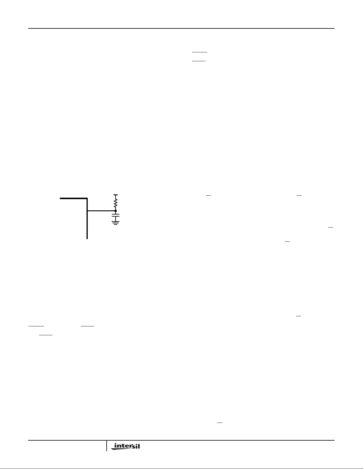
external resistor-capacitor circuit, as shown in Figure 3.
External clock sources (like those from a can oscillator)
should not be used with the CDP1020.
V
DD
26
CLK
Through the use of these pins, up to four devices may be
placed on the same bus (addresses $90, $92, $94, $96).
TEST
TEST is a CMOS input used only by Intersil for testing, and
is not recommended for the user; it must be externally
connected to V
DD
.
I2C/SMBus Interface
The CDP1020 contains a standard implementation of an
2
I
C/SMBus serial interface. The CDP1020 is always an
2
I
C/SMBus slave device. Its serial interface supports single
or burst mode reads and writes using standard I
mechanisms.
Reading from and Writing to the CDP1020
The I2C/SMBus slave address of the CDP1020 is
%10010XXY, where the “XX” bits are defined by the
AD1:AD0 input pins, and the “Y” is the R/W (Read/Write) bit.
Every access of the CDP1020 begins when the I
master generates a start condition (or repeated start
condition) followed b y tr ansmitting an address/control b yte
with the address equal to the CDP1020’s slave address and
the R/
W bit set appropriately . Note that the R/ W bit can be
considered the 8th (Least Significant Bit) in the address, even
though that may not be the standard I
2
C/SMBus notation.
2
C/SMBus
2
C/SMBus
CDP1020
FIGURE 3. RC OSCILLATOR CONFIGURATION
The CDP1020 is designed to operate optimally with an input
frequency of 4MHz. All of the internal timing, including
debounce, insertion delay, and solenoid pulse durations are
based on a 4MHz input. While the CDP1020 will operate
overa wide range of frequency, a nominal input frequency of
4MHz is strongly recommended. Refer to the
Interface
text at the end of this document for more
Hardware
information on the RC oscillator,including recommended RC
values.
ALRT (I2C/SMBus Alert Output)
The ALRT pin is the used by the CDP1020 to signal the
SMBus Host Controller that an interrupt event within the
controller has occurred and the device wishes to be read by
the operating system. This pin is an open drain output. Refer
to the
I2C/SMBus Interface
.
text for more details.
AD0, AD1
AD0 and AD1 are sampled by the CDP1020 immediately
after reset and are used as the 2 least significant bits of the
2
I
C/SMBus slave address of the CDP1020. These pins are
CMOS inputs, and should be tied to the same power plane
as the device (V
for a logic high; VSS for a logic low).
DD
A write operation is defined as the condition when the
2
I
C/SMBus master transmits the slaveaddress with the R/W
bit clear. A read operation is defined as the transmission of
the CDP1020 slave address with the R/
W bit set. Thus,
when looked upon as an 8-bit address, write operations will
have even addresses (for example, $90), while read
operations will be odd ($91).
For write operations, the command byte following the
address/control byte is used to set the internal
pointer
of the CDP1020. An I2C/SMBus
address
send byte
command
will therefore behave as a “set the address pointer”
command. The address pointer is initialized to $00 following
a reset. The byte written to the CDP1020 immediately
following an address/control byte with the R/
W bit clear will
always be used to set the CDP1020 internal address pointer.
Subsequent bytes written to the CDP1020 in a transmission
following the address/command and address pointer bytes
are written directly into the register space of the CDP1020.
The address pointer of the CDP1020 is auto-incrementing;
once a byte is written into the register space, the address
pointer increments to the next location. In this way multiple
byte writes to adjacent address locations within the
CDP1020 may be performed within a single I
2
C/SMBus
transmission. Figure 5 shows examples for a single byte and
a multiple byte write to the CDP1020.
Read operations are performed when the
I2C/SMBus master
transmits a start condition and the CDP1020 slave address
with the R/
W bit set. Following the address/command byte
2-424
 Loading...