

7-1259
CAUTION: These devices are sensitive to electrostatic discharge; follow proper IC Handling Procedures.
1-888-INTERSIL or 321-724-7143 | Copyright © Intersil Corporation 1999
CD4585BMS
CMOS 4-Bit Magnitude Comparator
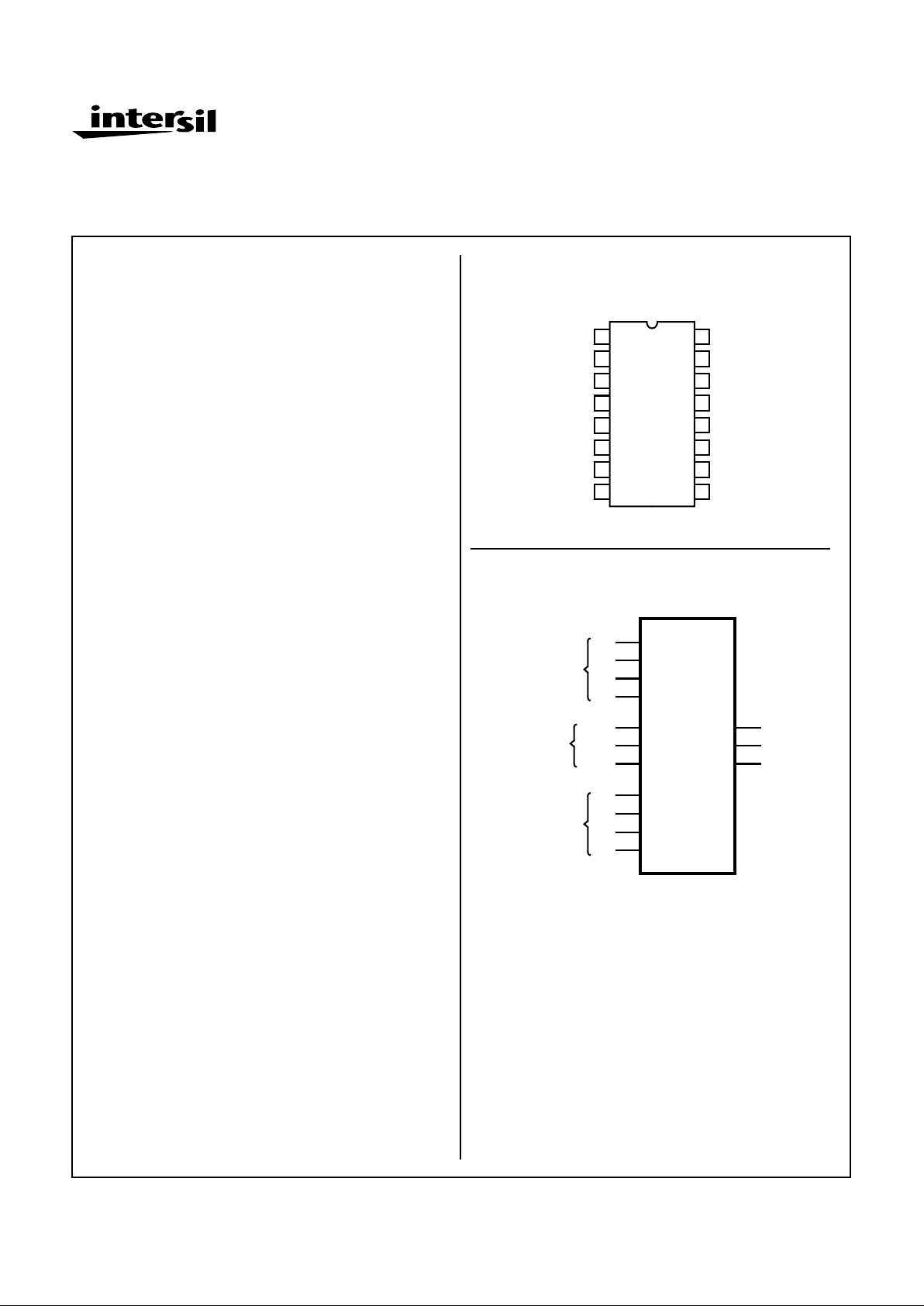
Pinout
CD4585BMS
TOP VIEW
Functional Diagram
14
15
16
9
13
12
11
10
1
2
3
4
5
7
6
8
B2
A2
(A = B)OUT
(A > B)IN
(A < B)IN
(A = B)IN
VSS
A1
VDD
B3
(A > B)OUT
(A < B)OUT
B0
A0
B1
A3
10
7
2
15
4
6
5
11
9
1
14
A0
A1
A2
A3
A > B
A = B
A < B
B0
B1
B2
B3
13
3
12
A > B
A = B
A < B
WORD “A”
CASCADING
INPUTS
WORD “B”
VDD = 16 VSS = 8
Features
• High Voltage Type (20V Rating)
• Expansion to 8, 12, 16 . . .4N Bits by Cascading Units
• Medium Speed Operation
- Compares Two 4-Bit Words in 180ns (Typ.) at 10V
• 100% Tested for Quiescent Current at 20V
• Standardized Symmetrical Output Characteristics
• 5V, 10V and 15V Parametric Ratings
• Maximum Input Current of 1µA at 18V Over Full Pack-
age Temperature Range; 100nA at 18V and +25oC
• Noise Margin (Over Full Package/Temperature Range)
- 1V at VDD = 5V
- 2V at VDD = 10V
- 2.5V at VDD = 15V
• Meets All Requirements of JEDEC Tentative Standard
No. 13B, “Standard Specifications for Description of
‘B’ Series CMOS Devices”
Applications
• Servo Motor Controls
• Process Controllers
Description
CD4585BMS is a 4-bit magnitude comparator designed for
use in computer and logic applications that require the comparison of two 4-bit words. This logic circuit determines
whether one 4-bit word (Binary or BCD) is “less than”, “equal
to” or “greater than” a second 4-bit word.
The CD4585BMS has eight comparing inputs (A3, B3,
through A0, B0), three outputs (A < B, = B, A > B) and three
cascading inputs (A < B, A = B, A > B) that permit system
designers to expand the comparator function to 8, 12, 16 . .
.4N bits. When a single CD4585BMS is used, the cascading
inputs are connected as follows: (A < B) = low, (A = B) =
high, (A > B) = high.
Cascading thses units for comparision of more than 4 bits is
accomplished as shown in Figure 9.
The CD4585BMS is supplied in these 16-lead outline packages:
Braze Seal DIP H4T
Frit Seal DIP H1E
Ceramic Flatpack H6W
December 1992
File Number
3347
7-1260
Specifications CD4585BMS
Absolute Maximum Ratings Reliability Information
DC Supply Voltage Range, (VDD) . . . . . . . . . . . . . . . -0.5V to +20V
(Voltage Referenced to VSS Terminals)
Input Voltage Range, All Inputs . . . . . . . . . . . . .-0.5V to VDD +0.5V
DC Input Current, Any One Input . . . . . . . . . . . . . . . . . . . . . . . .±10mA
Operating Temperature Range. . . . . . . . . . . . . . . . -55oC to +125oC
Package Types D, F, K, H
Storage Temperature Range (TSTG) . . . . . . . . . . . -65oC to +150oC
Lead Temperature (During Soldering) . . . . . . . . . . . . . . . . . +265oC
At Distance 1/16 ± 1/32 Inch (1.59mm ± 0.79mm) from case for
10s Maximum
Thermal Resistance . . . . . . . . . . . . . . . . θ
ja
θ
jc
Ceramic DIP and FRIT Package. . . . . 80oC/W 20oC/W
Flatpack Package . . . . . . . . . . . . . . . . 70oC/W 20oC/W
Maximum Package Power Dissipation (PD) at +125oC
For TA = -55oC to +100oC (Package Type D, F, K) . . . . . . 500mW
For TA = +100oC to +125oC (Package Type D, F, K). . . . . .Derate
Linearity at 12mW/oC to 200mW
Device Dissipation per Output Transistor . . . . . . . . . . . . . . . 100mW
For TA = Full Package Temperature Range (All Package Types)
Junction Temperature . . . . . . . . . . . . . . . . . . . . . . . . . . . . . . +175oC
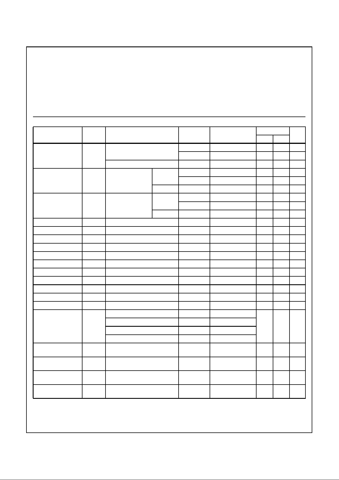
TABLE 1. DC ELECTRICAL PERFORMANCE CHARACTERISTICS
PARAMETER SYMBOL CONDITIONS (NOTE 1)
GROUP A
SUBGROUPS TEMPERATURE
LIMITS
UNITSMIN MAX
Supply Current IDD VDD = 20V, VIN = VDD or GND 1 +25oC-10µA
2 +125oC - 1000 µA
VDD = 18V, VIN = VDD or GND 3 -55oC-10µA
Input Leakage Current IIL VIN = VDD or GND VDD = 20 1 +25oC -100 - nA
2 +125oC -1000 - nA
VDD = 18V 3 -55oC -100 - nA
Input Leakage Current IIH VIN = VDD or GND VDD = 20 1 +25oC - 100 nA
2 +125oC - 1000 nA
VDD = 18V 3 -55oC - 100 nA
Output Voltage VOL15 VDD = 15V, No Load 1, 2, 3 +25oC, +125oC, -55oC - 50 mV
Output Voltage VOH15 VDD = 15V, No Load (Note 3) 1, 2, 3 +25oC, +125oC, -55oC 14.95 - V
Output Current (Sink) IOL5 VDD = 5V, VOUT = 0.4V 1 +25oC 0.53 - mA
Output Current (Sink) IOL10 VDD = 10V, VOUT = 0.5V 1 +25oC 1.4 - mA
Output Current (Sink) IOL15 VDD = 15V, VOUT = 1.5V 1 +25oC 3.5 - mA
Output Current (Source) IOH5A VDD = 5V, VOUT = 4.6V 1 +25oC - -0.53 mA
Output Current (Source) IOH5B VDD = 5V, VOUT = 2.5V 1 +25oC - -1.8 mA
Output Current (Source) IOH10 VDD = 10V, VOUT = 9.5V 1 +25oC - -1.4 mA
Output Current (Source) IOH15 VDD = 15V, VOUT = 13.5V 1 +25oC - -3.5 mA
N Threshold Voltage VNTH VDD = 10V, ISS = -10µA 1 +25oC -2.8 -0.7 V
P Threshold Voltage VPTH VSS = 0V, IDD = 10µA 1 +25oC 0.7 2.8 V
Functional F VDD = 2.8V, VIN = VDD or GND 7 +25oC VOH >
VDD/2
VOL <
VDD/2
V
VDD = 20V, VIN = VDD or GND 7 +25oC
VDD = 18V, VIN = VDD or GND 8A +125oC
VDD = 3V, VIN = VDD or GND 8B -55oC
Input Voltage Low
(Note 2)
VIL VDD = 5V, VOH > 4.5V, VOL < 0.5V 1, 2, 3 +25oC, +125oC, -55oC - 1.5 V
Input Voltage High
(Note 2)
VIH VDD = 5V, VOH > 4.5V, VOL < 0.5V 1, 2, 3 +25oC, +125oC, -55oC 3.5 - V
Input Voltage Low
(Note 2)
VIL VDD = 15V, VOH > 13.5V,
VOL < 1.5V
1, 2, 3 +25oC, +125oC, -55oC- 4 V
Input Voltage High
(Note 2)
VIH VDD = 15V, VOH > 13.5V,
VOL < 1.5V
1, 2, 3 +25oC, +125oC, -55oC11 - V
NOTES: 1. All voltages referenced to device GND, 100% testing being
implemented.
2. Go/No Go test with limits applied to inputs.
3. For accuracy, voltage is measured differentially to VDD. Limit
is 0.050V max.
7-1261
Specifications CD4585BMS
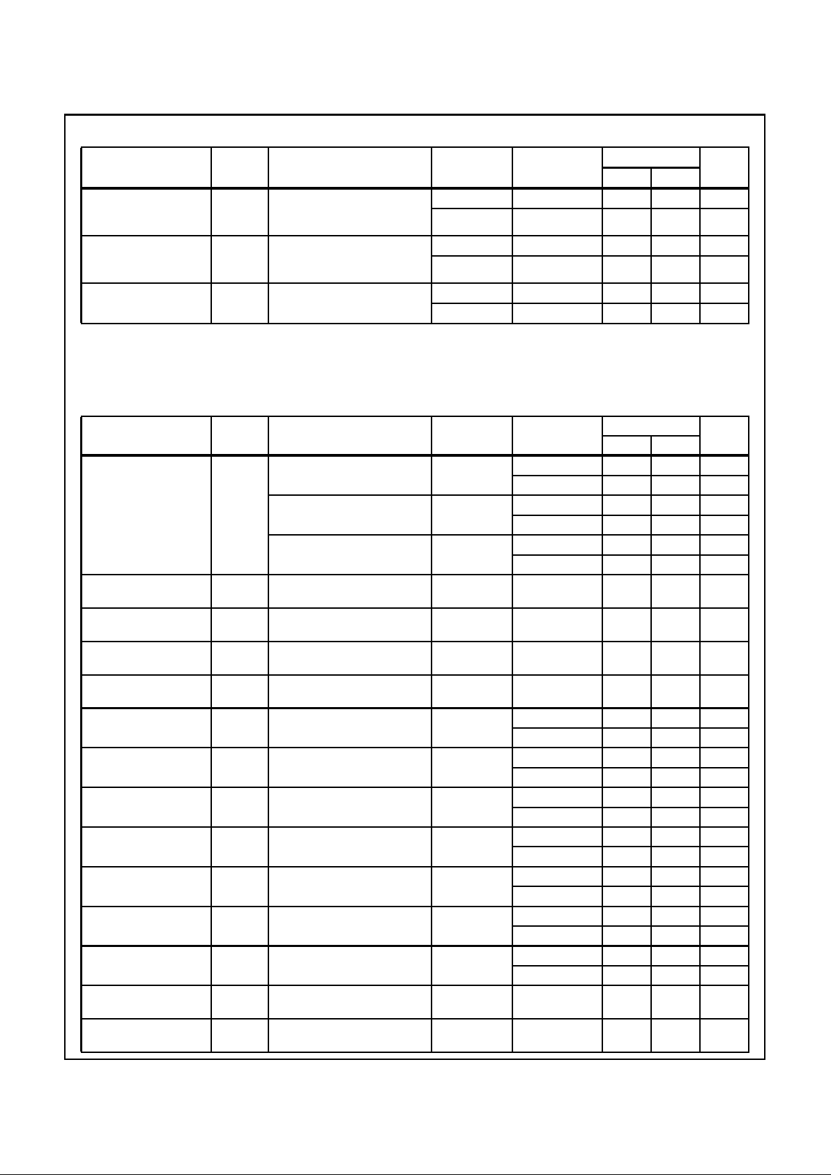
TABLE 2. AC ELECTRICAL PERFORMANCE CHARACTERISTICS
PARAMETER SYMBOL CONDITIONS (NOTE 1, 2)
GROUP A
SUBGROUPS TEMPERATURE
LIMITS
UNITSMIN MAX
Propagation Delay
Comparing
Inputs to Outputs
TPHL1
TPLH1
VDD = 5V, VIN = VDD or GND 9 +25oC - 600 ns
10, 11 +125oC, -55oC - 810 ns
Propagation Delay
Cascading Inputs to Outputs
TPHL2
TPLH2
VDD = 5V, VIN = VDD or GND 9 +25oC - 400 ns
10, 11 +125oC, -55oC - 540 ns
Transition Time TTHL
TTLH
VDD = 5V, VIN = VDD or GND 9 +25oC - 200 ns
10, 11 +125oC, -55oC - 270 ns
NOTES:
1. CL = 50pF, RL = 200K, Input TR, TF < 20ns.
2. -55oC and +125oC limits guaranteed, 100% testing being implemented.
TABLE 3. ELECTRICAL PERFORMANCE CHARACTERISTICS
PARAMETER SYMBOL CONDITIONS NOTES TEMPERATURE
LIMITS
UNITSMIN MAX
Supply Current IDD VDD = 5V, VIN = VDD or GND 1, 2 -55oC, +25oC- 5 µA
+125oC - 150 µA
VDD = 10V, VIN = VDD or GND 1, 2 -55oC, +25oC- 10µA
+125oC - 300 µA
VDD = 15V, VIN = VDD or GND 1, 2 -55oC, +25oC- 10µA
+125oC - 600 µA
Output Voltage VOL VDD = 5V, No Load 1, 2 +25oC, +125oC,
-55oC
-50mV
Output Voltage VOL VDD = 10V, No Load 1, 2 +25oC, +125oC,
-55oC
-50mV
Output Voltage VOH VDD = 5V, No Load 1, 2 +25oC, +125oC,
-55oC
4.95 - V
Output Voltage VOH VDD = 10V, No Load 1, 2 +25oC, +125oC,
-55oC
9.95 - V
Output Current (Sink) IOL5 VDD = 5V, VOUT = 0.4V 1, 2 +125oC 0.36 - mA
-55oC 0.64 - mA
Output Current (Sink) IOL10 VDD = 10V, VOUT = 0.5V 1, 2 +125oC 0.9 - mA
-55oC 1.6 - mA
Output Current (Sink) IOL15 VDD = 15V, VOUT = 1.5V 1, 2 +125oC 2.4 - mA
-55oC 4.2 - mA
Output Current (Source) IOH5A VDD = 5V, VOUT = 4.6V 1, 2 +125oC - -0.36 mA
-55oC - -0.64 mA
Output Current (Source) IOH5B VDD = 5V, VOUT = 2.5V 1, 2 +125oC - -1.15 mA
-55oC - -2.0 mA
Output Current (Source) IOH10 VDD = 10V, VOUT = 9.5V 1, 2 +125oC - -0.9 mA
-55oC - -1.6 mA
Output Current (Source) IOH15 VDD =15V, VOUT = 13.5V 1, 2 +125oC - -2.4 mA
-55oC - -4.2 mA
Input Voltage Low VIL VDD = 10V, VOH > 9V , VOL < 1V 1, 2 +25oC, +125oC,
-55oC
-3V
Input Voltage High VIH VDD = 10V , VOH > 9V, VOL < 1V 1, 2 +25oC, +125oC,
-55oC
+7 - V
7-1262
Specifications CD4585BMS
Propagation Delay
Comparing Inputs to
Outputs
TPHL1
TPLH1
VDD = 10V 1, 2, 3 +25oC - 250 ns
VDD = 15V 1, 2, 3 +25oC - 160 ns
Propagation Delay
Cascading Inputs to Outputs
TPHL2
TPLH2
VDD = 10V 1, 2, 3 +25oC - 160 ns
VDD = 15V 1, 2, 3 +25oC - 120 ns
Transition Time TTHL
TTLH
VDD = 10V 1, 2, 3 +25oC - 100 ns
VDD = 15V 1, 2, 3 +25oC - 80 ns
Input Capacitance CIN Any Inputs 1, 2 +25oC - 7.5 pF
NOTES:
1. All voltages referenced to device GND.
2. The parameters listed on Table 3 are controlled via design or process and are not directly tested. These parameters are characterized
on initial design release and upon design changes which would affect these characteristics.
3. CL = 50pF, RL = 200K, Input TR, TF < 20ns.
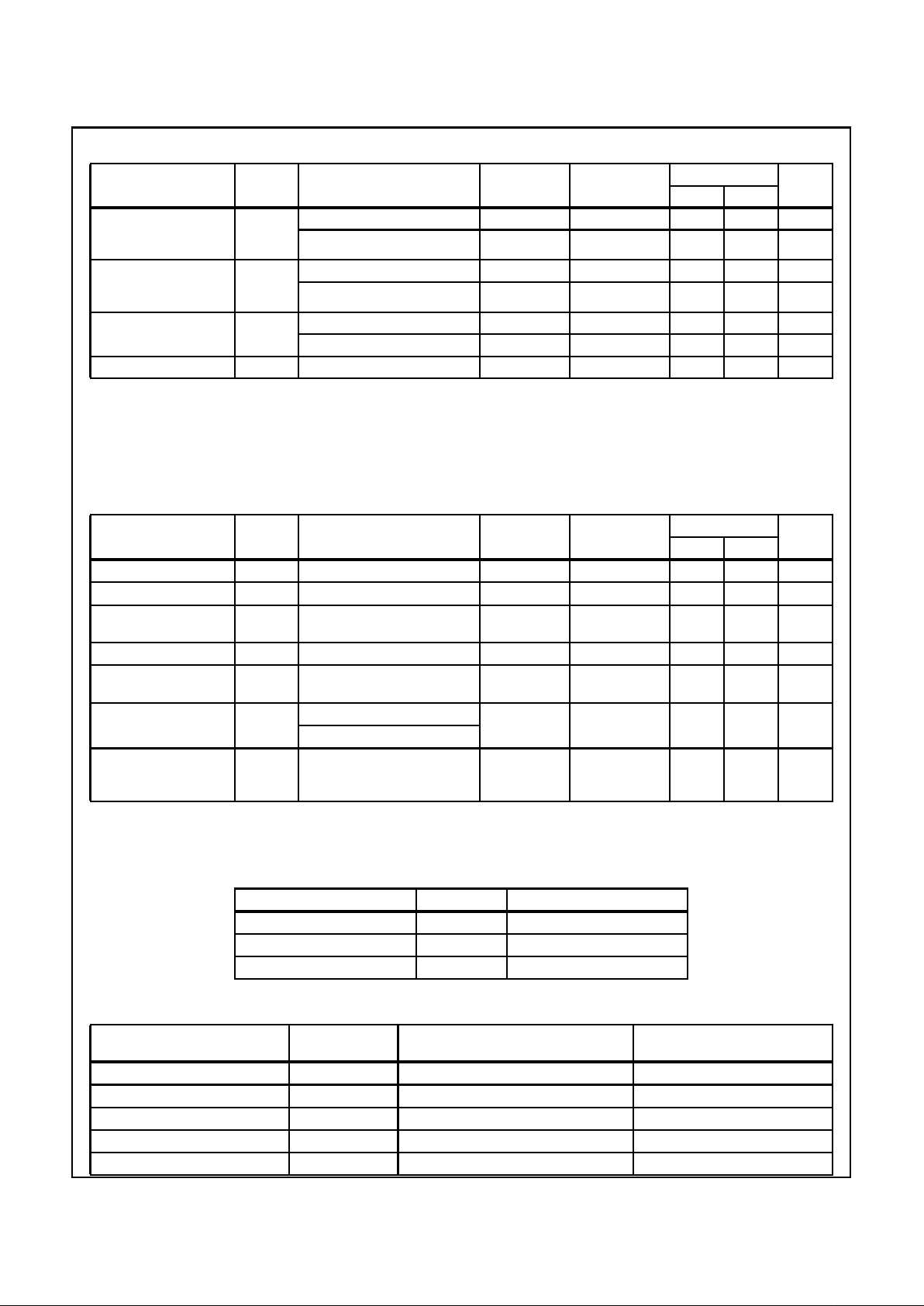
TABLE 4. POST IRRADIATION ELECTRICAL PERFORMANCE CHARACTERISTICS
PARAMETER SYMBOL CONDITIONS NOTES TEMPERATURE
LIMITS
UNITSMIN MAX
Supply Current IDD VDD = 20V, VIN = VDD or GND 1, 4 +25oC-25µA
N Threshold Voltage VNTH VDD = 10V, ISS = -10µA 1, 4 +25oC -2.8 -0.2 V
N Threshold Voltage
Delta
∆VTN VDD = 10V, ISS = -10µA 1, 4 +25oC-±1V
P Threshold Voltage VTP VSS = 0V, IDD = 10µA 1, 4 +25oC 0.2 2.8 V
P Threshold Voltage
Delta
∆VTP VSS = 0V, IDD = 10µA 1, 4 +25oC-±1V
Functional F VDD = 18V, VIN = VDD or GND 1 +25oC VOH >
VDD/2
VOL <
VDD/2
V
VDD = 3V, VIN = VDD or GND
Propagation Delay Time TPHL
TPLH
VDD = 5V 1, 2, 3, 4 +25oC - 1.35 x
+25oC
Limit
ns
NOTES: 1. All voltages referenced to device GND.
2. CL = 50pF, RL = 200K, Input TR, TF < 20ns.
3. See Table 2 for +25oC limit.
4. Read and Record
TABLE 5. BURN-IN AND LIFE TEST DELTA PARAMETERS +25oC
PARAMETER SYMBOL DELTA LIMIT
Supply Current - MSI-2 IDD ± 1.0µA
Output Current (Sink) IOL5 ± 20% x Pre-Test Reading
Output Current (Source) IOH5A ± 20% x Pre-Test Reading
TABLE 6. APPLICABLE SUBGROUPS
CONFORMANCE GROUP
MIL-STD-883
METHOD GROUP A SUBGROUPS READ AND RECORD
Initial Test (Pre Burn-In) 100% 5004 1, 7, 9 IDD, IOL5, IOH5A
Interim Test 1 (Post Burn-In) 100% 5004 1, 7, 9 IDD, IOL5, IOH5A
Interim Test 2 (Post Burn-In) 100% 5004 1, 7, 9 IDD, IOL5, IOH5A
PDA (Note 1) 100% 5004 1, 7, 9, Deltas
Interim Test 3 (Post Burn-In) 100% 5004 1, 7, 9 IDD, IOL5, IOH5A
TABLE 3. ELECTRICAL PERFORMANCE CHARACTERISTICS (Continued)
PARAMETER SYMBOL CONDITIONS NOTES TEMPERATURE
LIMITS
UNITSMIN MAX

1263
All Intersil semiconductor products are manufactured, assembled and tested under ISO9000 quality systems certification.
Intersil products are sold by description only. Intersil Corporation reserves the right to make changes in circuit design and/or specifications at any time without
notice. Accordingly, the reader is cautioned to verify that data sheets are current before placing orders. Information furnished by Intersil is believed to be accurate
and reliable. However, no responsibility is assumed by Intersil or its subsidiaries for its use; nor for any infringements of patents or other rights of third parties which
may result from its use. No license is granted by implication or otherwise under any patent or patent rights of Intersil or its subsidiaries.
For information regarding Intersil Corporation and its products, see web site http://www.intersil.com
Sales Office Headquarters
NORTH AMERICA
Intersil Corporation
P. O. Box 883, Mail Stop 53-204
Melbourne, FL 32902
TEL: (321) 724-7000
FAX: (321) 724-7240
EUROPE
Intersil SA
Mercure Center
100, Rue de la Fusee
1130 Brussels, Belgium
TEL: (32) 2.724.2111
FAX: (32) 2.724.22.05
ASIA
Intersil (Taiwan) Ltd.
Taiwan Limited
7F-6, No. 101 Fu Hsing North Road
Taipei, Taiwan
Republic of China
TEL: (886) 2 2716 9310
FAX: (886) 2 2715 3029
Specifications CD4585BMS
PDA (Note 1) 100% 5004 1, 7, 9, Deltas
Final Test 100% 5004 2, 3, 8A, 8B, 10, 11
Group A Sample 5005 1, 2, 3, 7, 8A, 8B, 9, 10, 11
Group B Subgroup B-5 Sample 5005 1, 2, 3, 7, 8A, 8B, 9, 10, 11, Deltas Subgroups 1, 2, 3, 9, 10, 11
Subgroup B-6 Sample 5005 1, 7, 9
Group D Sample 5005 1, 2, 3, 8A, 8B, 9 Subgroups 1, 2 3
NOTE: 1. 5% Parameteric, 3% Functional; Cumulative for Static 1 and 2.
TABLE 7. TOTAL DOSE IRRADIATION
CONFORMANCE GROUPS
MIL-STD-883
METHOD
TEST READ AND RECORD
PRE-IRRAD POST-IRRAD PRE-IRRAD POST-IRRAD
Group E Subgroup 2 5005 1, 7, 9 Table 4 1, 9 Table 4
TABLE 8. BURN-IN AND IRRADIATION TEST CONNECTIONS
FUNCTION OPEN GROUND VDD 9V ± -0.5V
OSCILLATOR
50kHz 25kHz
Static Burn-In 1
Note 1
3, 12, 13 1, 2, 4 - 11, 14, 15 16
Static Burn-In 2
Note 1
3, 12, 13 8 1, 2, 4 - 7, 9 - 11,
14 - 16
Dynamic BurnIn Note 1
- 5 - 9, 11, 14, 15 1, 4, 16 3, 12, 13 2 10
Irradiation
Note 2
3, 12, 13 8 1, 2, 4 - 7, 9 - 11,
14 - 16
NOTE:
1. Each pin except VDD and GND will have a series resistor of 10K ± 5%, VDD = 18V ± 0.5V
2. Each pin except VDD and GND will have a series resistor of 47K ± 5%; Group E, Subgroup 2, sample size is 4 dice/wafer, 0 failures,
VDD = 10V ± 0.5V
TABLE 6. APPLICABLE SUBGROUPS (Continued)
CONFORMANCE GROUP
MIL-STD-883
METHOD GROUP A SUBGROUPS READ AND RECORD

7-1264
CD4585BMS
Logic Diagram
FIGURE 1. LOGIC DIAGRAM
TRUTH TABLE
INPUTS
OUTPUTSCOMPARING CASCADING
A3, B3 A2, B2 A1, B1 A0, B0 A < B A = B A > B A < B A = B A > B
A3 > B3XXXXX1001
A3 = B3A2 > B2XXXX1001
A3 = B3A2 = B2A1 > B1XXX1001
A3 = B3A2 = B2A1 = B1A0 > B0XX1001
A3 = B3A2 = B2A1 = B1A0 = B0001001
A3 = B3 A2 = B2 A1 = B1 A0 = B0 0 1 X 0 1 0
A3 = B3 A2 = B2 A1 = B1 A0 = B0 1 0 X 1 0 0
A3 = B3 A2 = B2 A1 = B1 A0 < B0 X X X 1 0 0
A3 = B3A2 = B2A1 < B1XXXX100
A3 = B3A2 < B2XXXXX100
A3 < B3XXXXXX100
X = Don’t Care Logic 1 = High Level Logic 0 = Low Level
12
(A < B)OUT
(A = B)OUT
(A > B)OUT
3
13
15
14
2
1
7
9
10
11
5
6
4(A > B)IN
(A = B)IN
(A < B)IN
B0
A0
B1
A1
B2
A2
B3
A3
*
*
*
*
*
*
*
*
*
*
*
VDD
VSS
* INPUTS PROTECTED BY
CMOS PROTECTION
NETWORK

7-1265
CD4585BMS
Typical Performance Characteristics
FIGURE 2. TYPICAL OUTPUT LOW (SINK) CURRENT
CHARACTERISTICS
FIGURE 3. MINIMUM OUTPUT LOW (SINK) CURRENT
CHARACTERISTICS
FIGURE 4. TYPICAL OUTPUT HIGH (SOURCE) CURRENT
CHARACTERISTICS
FIGURE 5. MINIMUM OUTPUT HIGH (SOURCE) CURRENT
CHARACTERISTICS
FIGURE 6. TYPICAL TRANSITION TIME AS A FUNCTION OF
LOAD CAPACITANCE
FIGURE 7. TYPICAL PROPAGATION DELAY TIME (“COMPAR-
ING INPUTS” TO OUTPUTS) AS A FUNCTION OF
LOAD CAPACITANCE
10V
5V
AMBIENT TEMPERATURE (TA) = +25oC
GATE-TO-SOURCE VOLTAGE (VGS) = 15V
0 5 10 15
15
10
5
20
25
30
DRAIN-TO-SOURCE VOLTAGE (VDS) (V)
OUTPUT LOW (SINK) CURRENT (IOL) (mA)
10V
5V
AMBIENT TEMPERATURE (TA) = +25oC
GATE-TO-SOURCE VOLTAGE (VGS) = 15V
0 5 10 15
7.5
5.0
2.5
10.0
12.5
15.0
DRAIN-TO-SOURCE VOLTAGE (VDS) (V)
OUTPUT LOW (SINK) CURRENT (IOL) (mA)
-10V
-15V
AMBIENT TEMPERATURE (TA) = +25oC
GATE-TO-SOURCE VOLTAGE (VGS) = -5V
0
-5
-10
-15
DRAIN-TO-SOURCE VOLTAGE (VDS) (V)
-20
-25
-30
0-5-10-15
OUTPUT HIGH (SOURCE) CURRENT (IOH) (mA)
-10V
-15V
AMBIENT TEMPERATURE (TA) = +25oC
0
-5
-10
-15
DRAIN-TO-SOURCE VOLTAGE (VDS) (V)
0-5-10-15
OUTPUT HIGH (SOURCE) CURRENT (IOH) (mA)
GATE-TO-SOURCE VOLTAGE (VGS) = -5V
AMBIENT TEMPERATURE (TA) = +25oC
LOAD CAPACITANCE (CL) (pF)
0 40 60 80 10020
0
50
100
150
200
SUPPLY VOLTAGE (VDD) = 5V
10V
15V
TRANSITION TIME (tTHL, tTLH) (ns)
AMBIENT TEMPERATURE (TA) = +25oC
100
0
PROPAGATION DELAY TIME (tPHL, tPLH) (ns)
LOAD CAPACITANCE (CL) (pF)
SUPPLY VOLTAGE (VDD) = 5V
10V
15V
200
300
20 40 60 80 100

7-1266
CD4585BMS
FIGURE 9. TYPICAL SPEED CHARACTERISTICS OF A 12-BIT COMPARATOR
Chip Dimensions and Pad Layout
FIGURE 8. TYPICAL DYNAMIC POWER DISSIPATION AS A FUNCTION OF CLOCK INPUT FREQUENCY
Typical Performance Characteristics (Continued)
8642
CLOCK INPUT FREQUENCY (fIN) (kHz)
0.1
8
6
4
2
10
DYNAMIC POWER DISSIPATION (PD) (µW)
AMBIENT TEMPERATURE (TA) = +25oC
SUPPLY VOLTAGE (VDD) = 15V
10V
10V
5V
8
6
4
2
10
2
8
6
4
2
10
3
8
6
4
2
10
4
8642
1
8642
10
8642
10
2
8642
10
3
10
4
CL = 50pF
CL = 15pF
A4 A5 A6 A7
B4 B5 B6 B7
(A > B)OUT
(A = B)OUT
(A < B)OUT
A0 A1 A2 A3
(A > B)IN
(A = B)IN
(A < B)IN
CD4585BMS
B0 B1 B2 B3
CD4585BMS
A8 A9 A10 A11
B8 B9 B10 B11
CD4585BMS
VDD VDD VDD
tp TOTAL = tp (COMPARE)
INPUTS
+ 2 x tp (CASCADE)
INPUTS
, AT VDD = 10V
Dimensions in parenthese are in millimeters and are
derived from the basic inch dimensions as indicated.
Grid graduations are in mils (10
-3
inch).
METALLIZATION: Thickness: 11kÅ − 14kÅ, AL.
PASSIVATION: 10.4kÅ - 15.6kÅ, Silane
BOND PADS: 0.004 inches X 0.004 inches MIN
DIE THICKNESS: 0.0198 inches - 0.0218 inches
 Loading...