Intersil Corporation CD4536BMS Datasheet

CD4536BMS
December 1992
Features
• High Voltage Type (20V Rating)
0
24
• 24 Flip-Flop Stage - Counts from 2
• Last 16 Stages Selectable by BCD Select Code
• Bypass Input Allows Bypassing First 8 Stages
• On-Chip RC Oscillator Provision
• Clock Inhibit Input
• Schmitt Trigger in clock Line Permits Operation with
Very Long Rise and Fall Times
• On-Chip Monostable Output Provision
• Typical fCL = 3MHz at VDD = 10V
• Test Mode Allows Fast Test Sequence
• Set and Reset Inputs
• Capable of Driving Two Low Power TTL Loads, One
Lower Power Schottky Load, or Two HTL Loads Over
the Rated Temperature Range
• 100% Tested for Quiescent Current at 20V
• 5V, 10V and 15V Parametric Ratings
• Standardized, Symmetrical Output Characteristics
• Meets All Requirements of JEDEC Tentative Standard
No. 13B, “Standard Specifications for Description of
‘B’ Series CMOS Devices”
to 2
CMOS Programmable Timer
Description
CD4536BMS is a programmable timer consisting of 24 ripple
binary counter stages. The salient feature of this device is its
flexibility. The device can count from 1 to 2
stages can be bypassed to allow an output, selectable by a
4-bit code, from any one of the remaining 16 stages. It can
be driven by an external clock or an RC oscillator that can be
constructed using on-chip components. Input IN1 serves as
either the external clock input or the input to the on-chip RC
oscillator. OUT1 and OUT2 are connection terminals for the
external RC components. In addition, an on-chip monostable
circuit is provided to allow a variable pulse width output. V arious timing functions can be achieved using combinations of
these capabilities.
A logic 1 on the 8-BYPASS input enables a bypass of the
first 8 stages and makes stage 9 the first counter stage of
the last 16 stages. Selection of 1 of 16 outputs is accomplished by the decoder and the BCD inputs A, B, C and D.
MONO IN is the timing input for the on-chip monostable
oscillator. Grounding of the MONO IN terminal through a
resistor of 10kΩ or higher, disables the one-shot circuit and
connects the decoder directly to the DECODE OUT terminal.
A resistor to VDD and a capacitor to ground from the MONO
IN terminal enables the one-shot circuit and controls its
pulse width.
A fast test mode is enabled by a logic 1 on 8-BYPASS, SET,
and RESET. This mode divides the 24-stage counter into
three 8-stage sections to facilitate a fast test sequence.
The CD4536BMS is supplied in these 16-lead outline packages:
24
or the first 8
Braze Seal DIP H4X
Frit Seal DIP H1F
Ceramic Flatpack H6W
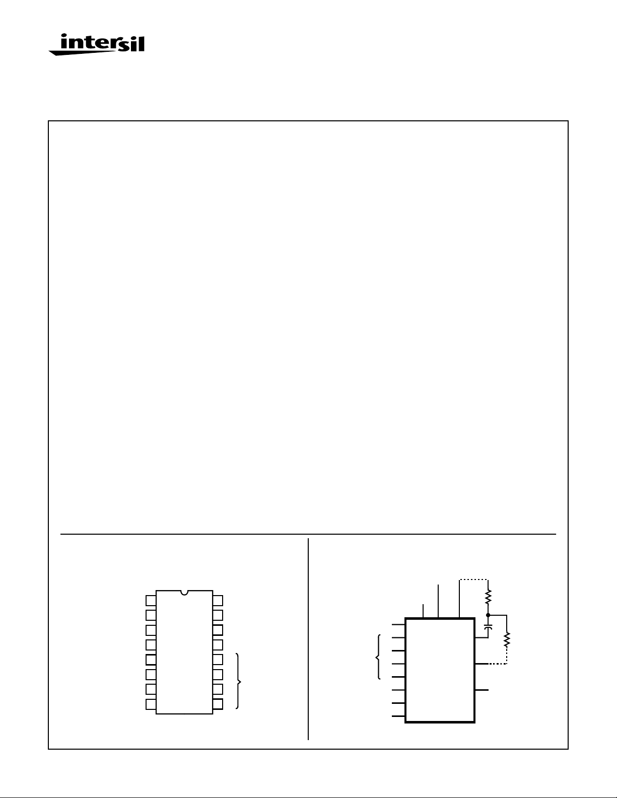
Pinout
CD4536BMS
TOP VIEW
16
1
SET
IN 1
OUT 1
OUT 2
VSS
2
3
4
5
6
7
8
RESET
8-BYPASS
CLOCK INHIBIT
CAUTION: These devices are sensitive to electrostatic discharge; follow proper IC Handling Procedures.
1-888-INTERSIL or 321-724-7143 | Copyright © Intersil Corporation 1999
VDD
15
MONO IN
14
OSC INHIBIT
13
DECODE OUT
12
D
11
C
10
B
9
A
BINARY
SELECT
Functional Diagram
BINARY
SELECT
RESET
MONO IN
7-1236
8-BYPASS
6
9
A
10
B
11
C
12
D
1
SET
2
15
CLOCK
INHIBIT
OSC
INHIBIT
14
IN 1
73
RS
4
OUT 1
5
OUT 2
13
RT
DECODE
OUT
VSS = 8
VDD = 16
File Number
3345

Specifications CD4536BMS
Absolute Maximum Ratings Reliability Information
DC Supply Voltage Range, (VDD) . . . . . . . . . . . . . . . -0.5V to +20V
(Voltage Referenced to VSS Terminals)
Input Voltage Range, All Inputs . . . . . . . . . . . . .-0.5V to VDD +0.5V
DC Input Current, Any One Input . . . . . . . . . . . . . . . . . . . . . . . .±10mA
Operating Temperature Range. . . . . . . . . . . . . . . . -55oC to +125oC
Package Types D, F, K, H
Storage Temperature Range (TSTG). . . . . . . . . . . -65oC to +150oC
Lead Temperature (During Soldering) . . . . . . . . . . . . . . . . . +265oC
At Distance 1/16 ± 1/32 Inch (1.59mm ± 0.79mm) from case for
10s Maximum
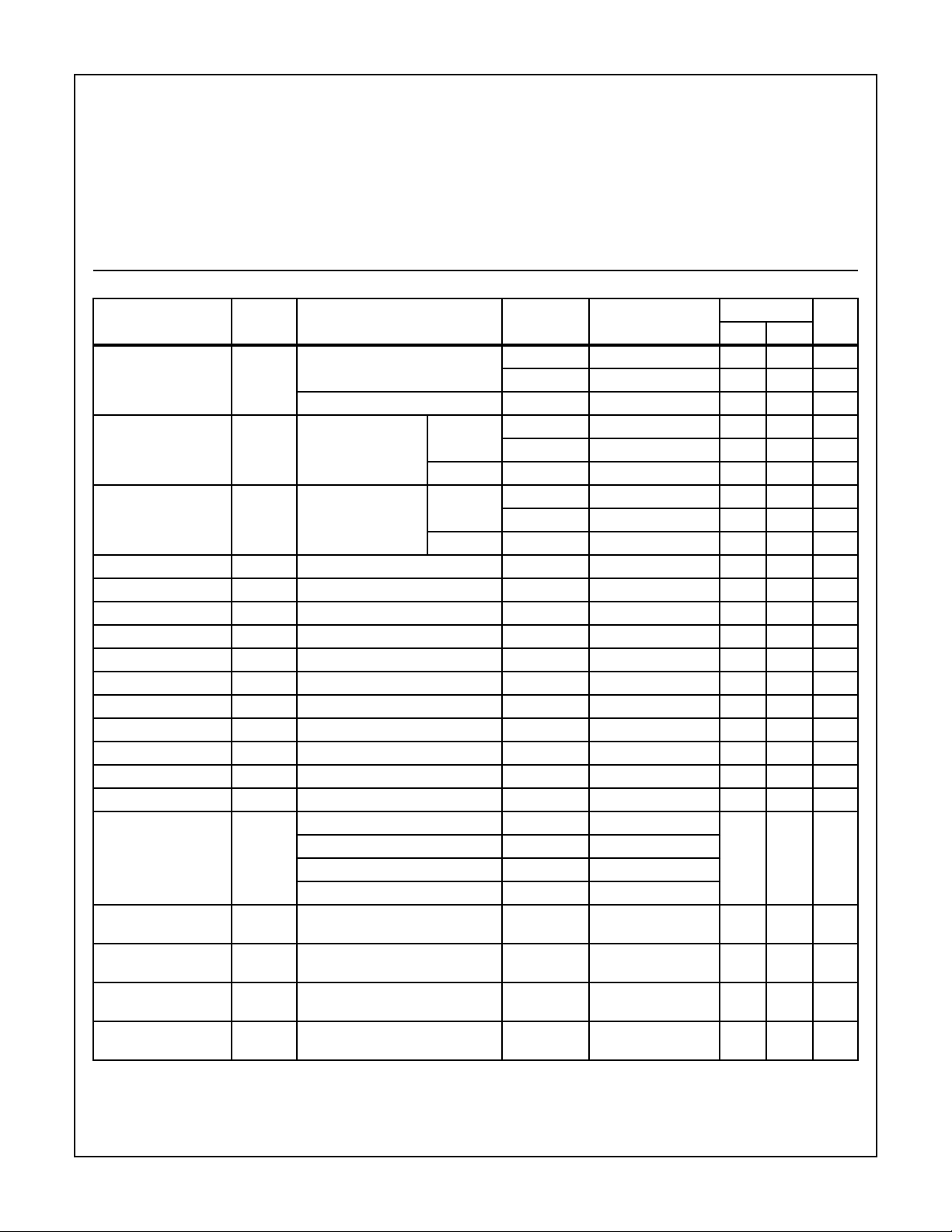
TABLE 1. DC ELECTRICAL PERFORMANCE CHARACTERISTICS
PARAMETER SYMBOL CONDITIONS (NOTE 1)
Supply Current IDD VDD = 20V, VIN = VDD or GND 1 +25oC-10µA
VDD = 18V, VIN = VDD or GND 3 -55oC-10µA
Input Leakage Current IIL VIN = VDD or GND VDD = 20 1 +25oC -100 - nA
VDD = 18V 3 -55oC -100 - nA
Input Leakage Current IIH VIN = VDD or GND VDD = 20 1 +25oC - 100 nA
VDD = 18V 3 -55oC - 100 nA
Output Voltage VOL15 VDD = 15V, No Load 1, 2, 3 +25oC, +125oC, -55oC - 50 mV
Output Voltage VOH15 VDD = 15V, No Load (Note 3) 1, 2, 3 +25oC, +125oC, -55oC 14.95 - V
Output Current (Sink) IOL5 VDD = 5V, VOUT = 0.4V 1 +25oC 0.53 - mA
Output Current (Sink) IOL10 VDD = 10V, VOUT = 0.5V 1 +25oC 1.4 - mA
Output Current (Sink) IOL15 VDD = 15V, VOUT = 1.5V 1 +25oC 3.5 - mA
Output Current (Source) IOH5A VDD = 5V, VOUT = 4.6V 1 +25oC - -0.53 mA
Output Current (Source) IOH5B VDD = 5V, VOUT = 2.5V 1 +25oC - -1.8 mA
Output Current (Source) IOH10 VDD = 10V, VOUT = 9.5V 1 +25oC - -1.4 mA
Output Current (Source) IOH15 VDD = 15V, VOUT = 13.5V 1 +25oC - -3.5 mA
N Threshold Voltage VNTH VDD = 10V, ISS = -10µA 1 +25oC -2.8 -0.7 V
P Threshold Voltage VPTH VSS = 0V, IDD = 10µA 1 +25oC 0.7 2.8 V
Functional F VDD = 2.8V, VIN = VDD or GND 7 +25oC VOH >
VDD = 20V, VIN = VDD or GND 7 +25oC
VDD = 18V, VIN = VDD or GND 8A +125oC
VDD = 3V, VIN = VDD or GND 8B -55oC
Input Voltage Low
(Note 2)
Input Voltage High
(Note 2)
Input Voltage Low
(Note 2)
Input Voltage High
(Note 2)
NOTES: 1. All voltages referenced to device GND, 100% testing being
implemented.
2. Go/No Go test with limits applied to inputs.
VIL VDD = 5V, VOH > 4.5V, VOL < 0.5V 1, 2, 3 +25oC, +125oC, -55oC - 1.5 V
VIH VDD = 5V, VOH > 4.5V, VOL < 0.5V 1, 2, 3 +25oC, +125oC, -55oC 3.5 - V
VIL VDD = 15V, VOH > 13.5V,
VOL < 1.5V
VIH VDD = 15V, VOH > 13.5V,
VOL < 1.5V
Thermal Resistance . . . . . . . . . . . . . . . . θ
Ceramic DIP and FRIT Package. . . . . 80oC/W 20oC/W
Flatpack Package . . . . . . . . . . . . . . . . 70oC/W 20oC/W
Maximum Package Power Dissipation (PD) at +125oC
For TA = -55oC to +100oC (Package Type D, F, K) . . . . . . 500mW
For TA = +100oC to +125oC (Package Type D, F, K). . . . . .Derate
Linearity at 12mW/oC to 200mW
Device Dissipation per Output Transistor . . . . . . . . . . . . . . . 100mW
For TA = Full Package Temperature Range (All Package Types)
Junction Temperature . . . . . . . . . . . . . . . . . . . . . . . . . . . . . . +175oC
GROUP A
SUBGROUPS TEMPERATURE
2 +125oC - 1000 µA
2 +125oC -1000 - nA
2 +125oC - 1000 nA
1, 2, 3 +25oC, +125oC, -55oC- 4 V
1, 2, 3 +25oC, +125oC, -55oC11 - V
3. For accuracy, voltage is measured differentially to VDD. Limit
is 0.050V max.
ja
LIMITS
VDD/2
VOL <
VDD/2
θ
jc
UNITSMIN MAX
V
7-1237

Specifications CD4536BMS
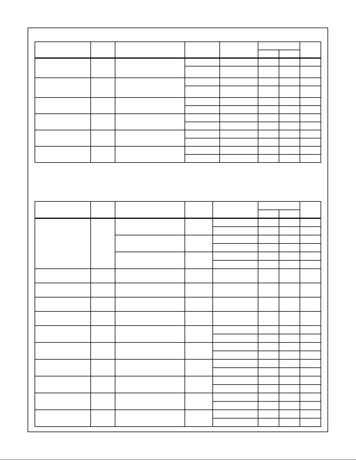
TABLE 2. AC ELECTRICAL PERFORMANCE CHARACTERISTICS
PARAMETER SYMBOL CONDITIONS (NOTE 1, 2)
Propagation Delay
Clock to Q1 8-Bypass
High
Propagation Delay
Clock to Q1 8-Bypass
Low
Propagation Delay
Clock to Q16
Propagation Delay
Reset to QN
Transition Time TTHL
Maximum Clock Input
Frequency
NOTES:
1. VDD = 5V, CL = 50pF, RL = 200K, Input TR, TF < 20ns.
2. -55oC and +125oC limits guaranteed, 100% testing being implemented.
TPHL1
TPLH1
TPHL2
TPLH2
TPHL3
TPLH3
TPHL4 VDD = 5V, VIN = VDD or GND 9 +25oC - 6000 ns
TTLH
FCL VDD = 5V, VIN = VDD or GND 9 +25oC .5 - MHz
VDD = 5V, VIN = VDD or GND 9 +25oC - 2000 ns
VDD = 5V, VIN = VDD or GND 9 +25oC - 5000 ns
VDD = 5V, VIN = VDD or GND 9 +25oC - 8000 ns
VDD = 5V, VIN = VDD or GND 9 +25oC - 200 ns
GROUP A
SUBGROUPS TEMPERATURE
10, 11 +125oC, -55oC - 2700 ns
10, 11 +125oC, -55oC - 6750 ns
10, 11 +125oC, -55oC - 10800 ns
10, 11 +125oC, -55oC - 8100 ns
10, 11 +125oC, -55oC - 270 ns
10, 11 +125oC, -55oC .37 - MHz
LIMITS
UNITSMIN MAX
TABLE 3. ELECTRICAL PERFORMANCE CHARACTERISTICS
LIMITS
PARAMETER SYMBOL CONDITIONS NOTES TEMPERATURE
o
Supply Current IDD VDD = 5V, VIN = VDD or GND 1, 2 -55
VDD = 10V, VIN = VDD or GND 1, 2 -55oC, +25oC-10µA
VDD = 15V, VIN = VDD or GND 1, 2 -55oC, +25oC-10µA
Output Voltage VOL VDD = 5V, No Load 1, 2 +25oC, +125oC, -
Output Voltage VOL VDD = 10V, No Load 1, 2 +25oC, +125oC, -
Output Voltage VOH VDD = 5V, No Load 1, 2 +25oC, +125oC, -
Output Voltage VOH VDD = 10V, No Load 1, 2 +25oC, +125oC, -
Output Current (Sink) IOL5 VDD = 5V, VOUT = 0.4V 1, 2 +125oC 0.36 - mA
Output Current (Sink) IOL10 VDD = 10V, VOUT = 0.5V 1, 2 +125oC 0.9 - mA
Output Current (Sink) IOL15 VDD = 15V, VOUT = 1.5V 1, 2 +125oC 2.4 - mA
Output Current (Source) IOH5A VDD = 5V, VOUT = 4.6V 1, 2 +125oC - -0.36 mA
Output Current (Source) IOH5B VDD = 5V, VOUT = 2.5V 1, 2 +125oC - -1.15 mA
Output Current (Source) IOH10 VDD = 10V, VOUT = 9.5V 1, 2 +125oC - -0.9 mA
C, +25oC-5µA
+125oC - 150 µA
+125oC - 300 µA
+125oC - 600 µA
-50mV
55oC
-50mV
55oC
4.95 - V
55oC
9.95 - V
55oC
-55oC 0.64 - mA
-55oC 1.6 - mA
-55oC 4.2 - mA
-55oC - -0.64 mA
-55oC - -2.0 mA
-55oC - -1.6 mA
UNITSMIN MAX
7-1238

Specifications CD4536BMS
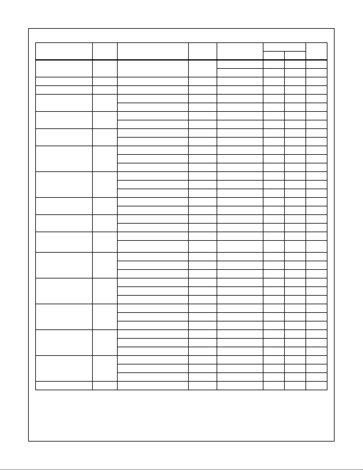
TABLE 3. ELECTRICAL PERFORMANCE CHARACTERISTICS
PARAMETER SYMBOL CONDITIONS NOTES TEMPERATURE
Output Current (Source) IOH15 VDD =15V, VOUT = 13.5V 1, 2 +125oC - -2.4 mA
Input Voltage Low VIL VDD = 10V, VOH > 9V , VOL < 1V 1, 2 +2 5oC, +125oC, -55oC- 3 V
Input Voltage High VIH VDD = 10V, VOH > 9V, VOL < 1V 1, 2 +2 5oC, +125oC, -55oC+7 - V
Propagation Delay
Clock to Q1 8-Bypass High
Propagation Delay
Clock to Q1 8-Bypass Low
Propagation Delay
Clock to Q16
Propagation Delay
Qn to Qn+1
Propagation Delay
Set to Qn
Propagation Delay
Reset to Qn
Transition Time TTHL
Maximum Clock Input
Frequency. Unlimited Input Rise or Fall Time
Minimum Clock Pulse
Width
Minimum Set Pulse Width TW VDD = 5V 1, 2, 3 +25oC - 400 ns
Minimum Reset Pulse
Width
Minimum Set Recovery
Time
Minimum Reset Recovery Time
Input Capacitance CIN Any Input 1, 2 +25oC - 7.5 pF
NOTES:
1. All voltages referenced to device GND.
2. The parameters listed on Table 3 are controlled via design or process and are not directly tested. These parameters are characterized
on initial design release and upon design changes which would affect these characteristics.
3. CL = 50pF, RL = 200K, Input TR, TF < 20ns.
TPHL1
TPLH1
TPHL2
TPLH2
TPHL3
TPLH3
TPHL
TPLH
TPLH VDD = 5V 1, 2, 3 +25oC - 600
TPHL4 VDD = 10V 1, 2, 3 +25oC - 2000 ns
TTLH
FCL VDD = 10V 1, 2, 3 +25oC 1.5 - MHz
TW VDD = 5V 1, 2, 3 +25oC - 400 ns
TW VDD = 5V 1, 2, 3 +25oC-6µs
TREM VDD = 5V 1, 2, 3 +25oC-5µs
TREM VDD = 5V 1, 2, 3 +25oC-7µs
VDD = 10V 1, 2, 3 +25oC - 1000 ns
VDD = 15V 1, 2, 3 +25oC - 700 ns
VDD = 10V 1, 2, 3 +25oC - 1600 ns
VDD = 15V 1, 2, 3 +25oC - 1200 ns
VDD = 10V 1, 2, 3 +25oC - 3000 ns
VDD = 15V 1, 2, 3 +25oC - 2000 ns
VDD = 5V 1, 2, 3 +25oC - 300
VDD = 10V 1, 2, 3 +25oC - 150
VDD = 15V 1, 2, 3 +25oC - 100
VDD = 10V 1, 2, 3 +25oC - 250
VDD = 15V 1, 2, 3 +25oC - 160
VDD = 15V 1, 2, 3 +25oC - 1500 ns
VDD = 10V 1, 2, 3 +25oC - 100 ns
VDD = 15V 1, 2, 3 +25oC - 80 ns
VDD = 15V 1, 2, 3 +25oC 2.5 - MHz
VDD = 10V 1, 2, 3 +25oC - 150 ns
VDD = 15V 1, 2, 3 +25oC - 100 ns
VDD = 10V 1, 2, 3 +25oC - 200 ns
VDD = 15V 1, 2, 3 +25oC - 120 ns
VDD = 10V 1, 2, 3 +25oC-2µs
VDD = 15V 1, 2, 3 +25oC - 1.5 µs
VDD = 10V 1, 2, 3 +25oC-2µs
VDD = 15V 1, 2, 3 +25oC - 1.6 µs
VDD = 10V 1, 2, 3 +25oC-3µs
VDD = 15V 1, 2, 3 +25oC-2µs
(Continued)
LIMITS
UNITSMIN MAX
-55oC - -4.2 mA
7-1239
 Loading...