

CD4527BMS
December 1992
Features
• High Voltage Type (20V Rating)
• Cascadable in Multiples of 4-Bits
• Set to “9” Input and “9” Detect Output
• 100% Tested for Quiescent Current at 20V
• 5V, 10V and 15V Parametric Ratings
• Maximum Input Current of 1µA at 18V Over Full Pack-
age Temperature Range; 100nA at 18V and +25
• Noise Margin (Over Full Package/Temperature Range)
- 1V at VDD = 5V
- 2V at VDD = 10V
- 2.5V at VDD = 15V
• Standardized Symmetrical Output Characteristics
• Meets All Requirements of JEDEC Tentative Standard
No. 13B, “Standard Specifications for Description of
‘B’ Series CMOS Devices”
Applications
• Numerical Control
• Instrumentation
• Digital Filtering
• Frequency Synthesis
CMOS BCD Rate Multiplier
Description
CD4527BMS is a low power 4-bit digital rate multiplier that
provides an output pulse rate which is the clock input pulse
rate multiplied by 1/10 times the BCD input. For example,
when the BCD input is 8, there will be 8 output pulses for
every 10 input pulses. This device may be used to perform
arithmetic operations (add, subtract, divide, raise to a
power), solve algebraic and differential equations, generate
natural logarithms and trigonometric functions, A/D and D/A
o
C
conversion, and frequency division.
For fractional multipliers with more than one digit,
CD4527BMS devices may be cascaded in two different
modes: the Add mode and the Multiply mode (see Figures 9
and 11). In the Add mode,
Output Rate =
(Clock Rate) [0.1BCD1 + 0.01BCD2 + 0.001BCD3 + . . .]
In the Multiply mode, the fraction programmed into the first
rate multiplier is multiplied by the fraction programmed into
the second one,
9
e.g.
10 10 100
4
x
36
=
or 36 output
pulses for every 100 clock input pulses.
The CD4527BMS is supplied in these 16-lead outline packages:
Braze Seal DIP H4X
Frit Seal DIP H1F
Ceramic Flatpack H6W
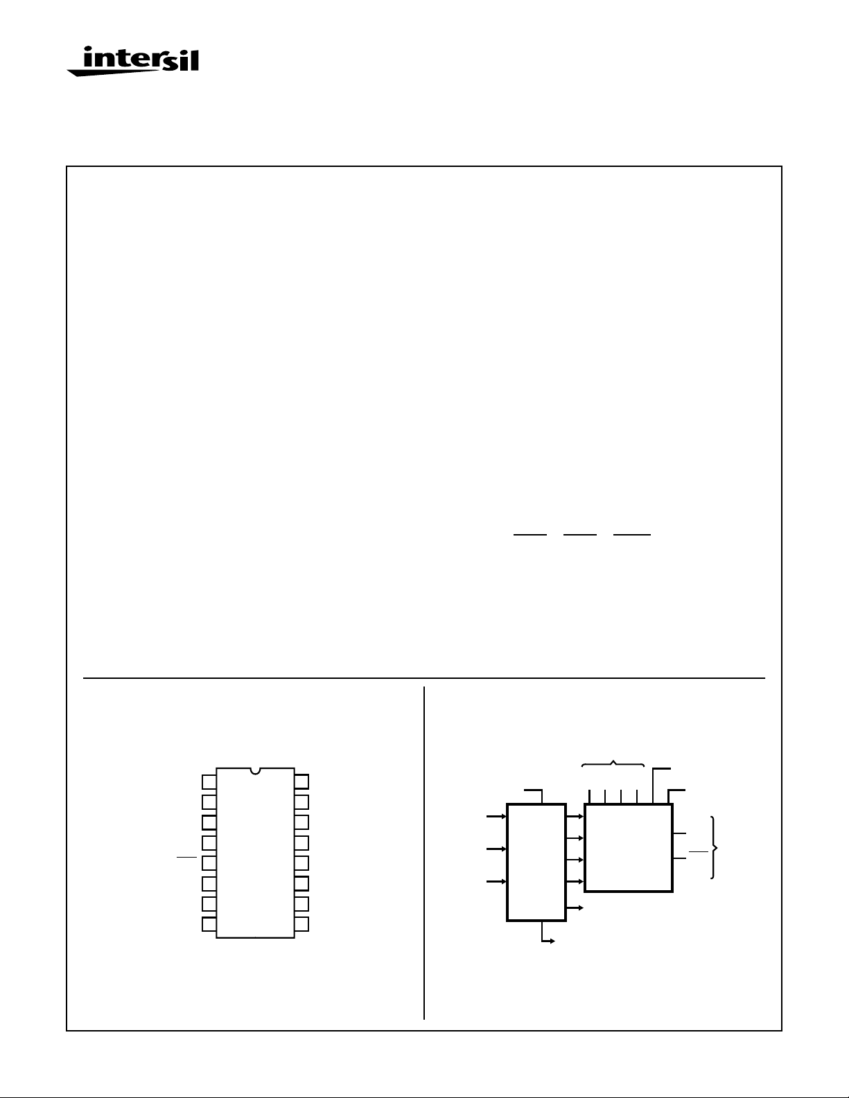
Pinout
CD4527BMS
TOP VIEW
VDD
16
15
B
A
14
CLEAR
13
CASCADE
12
INHIBIT IN (CARRY)
11
STROBE
10
9
CLOCK
OUT
OUT
VSS
1
2
C
3
D
4
5
6
7
8
“9” OUT
SET TO “9”
INHIBIT OUT (CARRY)
CAUTION: These devices are sensitive to electrostatic discharge; follow proper IC Handling Procedures.
1-888-INTERSIL or 321-724-7143 | Copyright © Intersil Corporation 1999
Functional Diagram
CLOCK
11
INHIBIT
(CARRY) IN
4
SET TO
NINE
13
CLEAR
7-1216
9
÷10
COUNTER
7
BCD RATE
SELECT INPUTS
A
14B15C2D3
RATE
SELECT
LOGIC
“9” OUT
1
INHIBIT
(CARRY) OUT
STROBE
10
CASCADE
12
OUT
6
RATE
OUTPUTS
OUT
5
VSS = 8
VDD = 16
File Number 3343
Specifications CD4527BMS
Absolute Maximum Ratings Reliability Information
DC Supply Voltage Range, (VDD) . . . . . . . . . . . . . . . -0.5V to +20V
(Voltage Referenced to VSS Terminals)
Input Voltage Range, All Inputs . . . . . . . . . . . . .-0.5V to VDD +0.5V
DC Input Current, Any One Input . . . . . . . . . . . . . . . . . . . . . . . .±10mA
Operating Temperature Range. . . . . . . . . . . . . . . . -55oC to +125oC
Package Types D, F, K, H
Storage Temperature Range (TSTG) . . . . . . . . . . . -65oC to +150oC
Lead Temperature (During Soldering) . . . . . . . . . . . . . . . . . +265oC
At Distance 1/16 ± 1/32 Inch (1.59mm ± 0.79mm) from case for
10s Maximum
TABLE 1. DC ELECTRICAL PERFORMANCE CHARACTERISTICS
PARAMETER SYMBOL CONDITIONS (NOTE 1)
Supply Current IDD VDD = 20V, VIN = VDD or GND 1 +25oC-10µA
VDD = 18V, VIN = VDD or GND 3 -55oC-10µA
Input Leakage Current IIL VIN = VDD or GND VDD = 20 1 +25oC -100 - nA
VDD = 18V 3 -55oC -100 - nA
Input Leakage Current IIH VIN = VDD or GND VDD = 20 1 +25oC - 100 nA
VDD = 18V 3 -55oC - 100 nA
Output Voltage VOL15 VDD = 15V, No Load 1, 2, 3 +25oC, +125oC, -55oC - 50 mV
Output Voltage VOH15 VDD = 15V, No Load (Note 3) 1, 2, 3 +25oC, +125oC, -55oC 14.95 - V
Output Current (Sink) IOL5 VDD = 5V, VOUT = 0.4V 1 +25oC 0.53 - mA
Output Current (Sink) IOL10 VDD = 10V, VOUT = 0.5V 1 +25oC 1.4 - mA
Output Current (Sink) IOL15 VDD = 15V, VOUT = 1.5V 1 +25oC 3.5 - mA
Output Current (Source) IOH5A VDD = 5V, VOUT = 4.6V 1 +25oC - -0.53 mA
Output Current (Source) IOH5B VDD = 5V, VOUT = 2.5V 1 +25oC - -1.8 mA
Output Current (Source) IOH10 VDD = 10V, VOUT = 9.5V 1 +25oC - -1.4 mA
Output Current (Source) IOH15 VDD = 15V, VOUT = 13.5V 1 +25oC - -3.5 mA
N Threshold Voltage VNTH VDD = 10V, ISS = -10µA 1 +25oC -2.8 -0.7 V
P Threshold Voltage VPTH VSS = 0V, IDD = 10µA 1 +25oC 0.7 2.8 V
Functional F VDD = 2.8V, VIN = VDD or GND 7 +25oC VOH >
VDD = 20V, VIN = VDD or GND 7 +25oC
VDD = 18V, VIN = VDD or GND 8A +125oC
VDD = 3V, VIN = VDD or GND 8B -55oC
Input Voltage Low
(Note 2)
Input Voltage High
(Note 2)
Input Voltage Low
(Note 2)
Input Voltage High
(Note 2)
NOTES: 1. All voltages referenced to device GND, 100% testing being
implemented.
2. Go/No Go test with limits applied to inputs.
VIL VDD = 5V, VOH > 4.5V, VOL < 0.5V 1, 2, 3 +25oC, +125oC, -55oC - 1.5 V
VIH VDD = 5V, VOH > 4.5V, VOL < 0.5V 1, 2, 3 +25oC, +125oC, -55oC 3.5 - V
VIL VDD = 15V, VOH > 13.5V,
VOL < 1.5V
VIH VDD = 15V, VOH > 13.5V,
VOL < 1.5V
Thermal Resistance . . . . . . . . . . . . . . . . θ
Ceramic DIP and FRIT Package. . . . . 80oC/W 20oC/W
Flatpack Package . . . . . . . . . . . . . . . . 70oC/W 20oC/W
Maximum Package Power Dissipation (PD) at +125oC
For TA = -55oC to +100oC (Package Type D, F, K) . . . . . . 500mW
For TA = +100oC to +125oC (Package Type D, F, K). . . . . .Derate
Linearity at 12mW/oC to 200mW
Device Dissipation per Output Transistor . . . . . . . . . . . . . . . 100mW
For TA = Full Package Temperature Range (All Package Types)
Junction Temperature . . . . . . . . . . . . . . . . . . . . . . . . . . . . . . +175oC
GROUP A
SUBGROUPS TEMPERATURE
2 +125oC - 1000 µA
2 +125oC -1000 - nA
2 +125oC - 1000 nA
1, 2, 3 +25oC, +125oC, -55oC- 4 V
1, 2, 3 +25oC, +125oC, -55oC11 - V
3. For accuracy, voltage is measured differentially to VDD. Limit
is 0.050V max.
ja
LIMITS
VDD/2
VOL <
VDD/2
θ
jc
UNITSMIN MAX
V
7-1217

Specifications CD4527BMS
TABLE 2. AC ELECTRICAL PERFORMANCE CHARACTERISTICS
GROUP A
PARAMETER SYMBOL CONDITIONS (NOTE 1, 2)
Propagation Delay
Clock to Output
Propagation Delay
Clear to Output
Propagation Delay
Cascade to Output
Transition Time TTHL
Maximum Clock Input
Frequency
NOTES:
1. CL = 50pF, RL = 200K, Input TR, TF < 20ns.
2. -55oC and +125oC limits guaranteed, 100% testing being implemented.
PARAMETER SYMBOL CONDITIONS NOTES TEMPERATURE
Supply Current IDD VDD = 5V, VIN = VDD or GND 1, 2 -55oC, +25oC- 5 µA
Output Voltage VOL VDD = 5V, No Load 1, 2 +25oC, +125oC,
Output Voltage VOL VDD = 10V, No Load 1, 2 +25oC, +125oC,
Output Voltage VOH VDD = 5V, No Load 1, 2 +25oC, +125oC,
Output Voltage VOH VDD = 10V, No Load 1, 2 +25oC, +125oC,
Output Current (Sink) IOL5 VDD = 5V, VOUT = 0.4V 1, 2 +125oC 0.36 - mA
Output Current (Sink) IOL10 VDD = 10V, VOUT = 0.5V 1, 2 +125oC 0.9 - mA
Output Current (Sink) IOL15 VDD = 15V, VOUT = 1.5V 1, 2 +125oC 2.4 - mA
Output Current (Source) IOH5A VDD = 5V, VOUT = 4.6V 1, 2 +125oC - -0.36 mA
Output Current (Source) IOH5B VDD = 5V, VOUT = 2.5V 1, 2 +125oC - -1.15 mA
Output Current (Source) IOH10 VDD = 10V, VOUT = 9.5V 1, 2 +125oC - -0.9 mA
Output Current (Source) IOH15 VDD =15V, VOUT = 13.5V 1, 2 +125oC - -2.4 mA
Input Voltage Low VIL VDD = 10V, VOH > 9V , VOL < 1V 1, 2 +25oC, +125oC,
TPHL1
TPLH1
TPHL2
TPLH2
TPHL3
TPLH3
TTLH
FCL VDD = 5V, VIN = VDD or GND 9 +25oC 1.2 - MHz
VDD = 5V, VIN = VDD or GND 9 +25oC - 300 ns
VDD = 5V, VIN = VDD or GND 9 +25oC - 760 ns
VDD = 5V, VIN = VDD or GND 9 +25oC - 180 ns
VDD = 5V, VIN = VDD or GND 9 +25oC - 200 ns
TABLE 3. ELECTRICAL PERFORMANCE CHARACTERISTICS
VDD = 10V, VIN = VDD or GND 1, 2 -55oC, +25oC- 10µA
VDD = 15V, VIN = VDD or GND 1, 2 -55oC, +25oC- 10µA
SUBGROUPS TEMPERATURE
10, 11 +125oC, -55oC - 405 ns
10, 11 +125oC, -55oC - 1026 ns
10, 11 +125oC, -55oC - 243 ns
10, 11 +125oC, -55oC - 270 ns
10, 11 +125oC, -55oC .89 - MHz
+125oC - 150 µA
+125oC - 300 µA
+125oC - 600 µA
-55oC
-55oC
-55oC
-55oC
-55oC 0.64 - mA
-55oC 1.6 - mA
-55oC 4.2 - mA
-55oC - -0.64 mA
-55oC - -2.0 mA
-55oC - -1.6 mA
-55oC - -4.2 mA
-55oC
LIMITS
UNITSMIN MAX
LIMITS
UNITSMIN MAX
-50mV
-50mV
4.95 - V
9.95 - V
-3V
7-1218
Specifications CD4527BMS
TABLE 3. ELECTRICAL PERFORMANCE CHARACTERISTICS (Continued)
PARAMETER SYMBOL CONDITIONS NOTES TEMPERATURE
Input Voltage High VIH VDD = 10V, VOH > 9V, VOL < 1V 1, 2 +25oC, +125oC,
-55oC
Propagation Delay
Clock to Output
Propagation Delay
Clear to Output
Propagation Delay
Cascade to Output
Propagation Delay
Clock to Out
Propagation Delay
Clock to INHIBIT Out
Propagation Delay
Clock to INHIBIT Out
Propagation Delay
INHIBIT IN to
INHIBIT Out
Propagation Delay
Clock to “9” or “15” Out
Propagation Delay
Set to Out
Transition Time TTHL
Maximum Clock Input
Frequency
Minimum Data Setup
Time - Inhibit
Minimum Inhibit Removal
Time
Minimum Clock Pulse
Width
Maximum Clock Rise and
Fall Time
TPHL1
TPLH1
TPHL2
TPLH2
TPHL3
TPLH3
TPHL
TPLH
TPHL VDD = 5V 1, 2, 3 +25oC - 640 ns
TPLH VDD = 5V 1, 2, 3 +25oC - 500 ns
TPHL
TPLH
TPHL
TPLH
TPHL
TPLH
TTLH
FCL VDD = 10V 1, 2 +25oC 2.5 - MHz
TREM VDD = 5V 1, 2, 3 +25oC - 240 ns
TW VDD = 5V 1, 2, 3 +25oC - 330 ns
TRCL
TFCL
VDD = 10V 1, 2, 3 +25oC - 150 ns
VDD = 15V 1, 2, 3 +25oC - 120 ns
VDD = 10V 1, 2, 3 +25oC - 350 ns
VDD = 15V 1, 2, 3 +25oC - 260 ns
VDD = 10V 1, 2, 3 +25oC - 90 ns
VDD = 15V 1, 2, 3 +25oC - 70 ns
VDD = 5V 1, 2, 3 +25oC - 220 ns
VDD = 10V 1, 2, 3 +25oC - 110 ns
VDD = 15V 1, 2, 3 +25oC - 90 ns
VDD = 10V 1, 2, 3 +25oC - 290 ns
VDD = 15V 1, 2, 3 +25oC - 200 ns
VDD = 10V 1, 2, 3 +25oC - 200 ns
VDD = 15V 1, 2, 3 +25oC - 150 ns
VDD = 5V 1, 2, 3 +25oC - 260 ns
VDD = 10V 1, 2, 3 +25oC - 120 ns
VDD = 15V 1, 2, 3 +25oC - 90 ns
VDD = 5V 1, 2, 3 +25oC - 600 ns
VDD = 10V 1, 2, 3 +25oC - 250 ns
VDD = 15V 1, 2, 3 +25oC - 180 ns
VDD = 5V 1, 2, 3 +25oC - 660 ns
VDD = 10V 1, 2, 3 +25oC - 300 ns
VDD = 15V 1, 2, 3 +25oC - 220 ns
VDD = 10V 1, 2, 3 +25oC - 100 ns
VDD = 15V 1, 2, 3 +25oC - 80 ns
VDD = 15V 1, 2 +25oC 3.5 - MHz
TS VDD = 5V 1, 2, 3 +25oC - 100 ns
VDD = 10V 1, 2, 3 +25oC - 40 ns
VDD = 15V 1, 2, 3 +25oC - 20 ns
VDD = 10V 1, 2, 3 +25oC - 130 ns
VDD = 15V 1, 2, 3 +25oC - 110 ns
VDD = 10V 1, 2, 3 +25oC - 170 ns
VDD = 15V 1, 2, 3 +25oC - 100 ns
VDD = 5V 1, 2, 3, 4 +25oC-15µs
VDD = 10V 1, 2, 3, 4 +25oC-15µs
VDD = 15V 1, 2, 3, 4 +25oC-15µs
LIMITS
UNITSMIN MAX
+7 - V
7-1219

Specifications CD4527BMS
TABLE 3. ELECTRICAL PERFORMANCE CHARACTERISTICS (Continued)
LIMITS
PARAMETER SYMBOL CONDITIONS NOTES TEMPERATURE
Minimum Clear Removal
Time
Minimum Set Removal
Time
Minimum Set or Clear
Pulse Width
Input Capacitance CIN Any Input 1, 2 +25oC - 7.5 pF
NOTES:
1. All voltages referenced to device GND.
2. The parameters listed on Table 3 are controlled via design or process and are not directly tested. These parameters are characterized
on initial design release and upon design changes which would affect these characteristics.
3. CL = 50pF, RL = 200K, Input TR, TF < 20ns.
4. If more than one unit is cascaded, TRCL should be made less than or equal to the sumof the transition time and the fixed propagation
delay of the output of the driving stage for the estimated capacitive load.
TREM VDD = 5V 1, 2, 3 +25oC - 60 ns
VDD = 10V 1, 2, 3 +25oC - 40 ns
VDD = 15V 1, 2, 3 +25oC - 30 ns
TREM VDD = 5V 1, 2, 3 +25oC - 150 ns
VDD = 10V 1, 2, 3 +25oC - 80 ns
VDD = 15V 1, 2, 3 +25oC - 50 ns
TW VDD = 5V 1, 2, 3 +25oC - 160 ns
VDD = 10V 1, 2, 3 +25oC - 90 ns
VDD = 15V 1, 2, 3 +25oC - 60 ns
UNITSMIN MAX
TABLE 4. POST IRRADIATION ELECTRICAL PERFORMANCE CHARACTERISTICS
LIMITS
PARAMETER SYMBOL CONDITIONS NOTES TEMPERATURE
Supply Current IDD VDD = 20V, VIN = VDD or GND 1, 4 +25oC-25µA
N Threshold Voltage VNTH VDD = 10V, ISS = -10µA 1, 4 +25oC -2.8 -0.2 V
N Threshold Voltage
Delta
P Threshold Voltage VTP VSS = 0V, IDD = 10µA 1, 4 +25oC 0.2 2.8 V
P Threshold Voltage
Delta
Functional F VDD = 18V, VIN = VDD or GND 1 +25oC VOH >
Propagation Delay Time TPHL
NOTES: 1. All voltages referenced to device GND.
2. CL = 50pF, RL = 200K, Input TR, TF < 20ns.
∆VTN VDD = 10V, ISS = -10µA 1, 4 +25oC-±1V
∆VTP VSS = 0V, IDD = 10µA 1, 4 +25oC-±1V
VOL <
VDD = 3V, VIN = VDD or GND
VDD = 5V 1, 2, 3, 4 +25oC - 1.35 x
TPLH
3. See Table 2 for +25oC limit.
4. Read and Record
TABLE 5. BURN-IN AND LIFE TEST DELTA PARAMETERS +25oC
PARAMETER SYMBOL DELTA LIMIT
Supply Current - MSI-2 IDD ± 1.0µA
Output Current (Sink) IOL5 ± 20% x Pre-Test Reading
Output Current (Source) IOH5A ± 20% x Pre-Test Reading
VDD/2
VDD/2
+25oC
Limit
UNITSMIN MAX
ns
V
TABLE 6. APPLICABLE SUBGROUPS
MIL-STD-883
CONFORMANCE GROUP
Initial Test (Pre Burn-In) 100% 5004 1, 7, 9 IDD, IOL5, IOH5A
Interim Test 1 (Post Burn-In) 100% 5004 1, 7, 9 IDD, IOL5, IOH5A
Interim Test 2 (Post Burn-In) 100% 5004 1, 7, 9 IDD, IOL5, IOH5A
METHOD GROUP A SUBGROUPS READ AND RECORD
7-1220

Specifications CD4527BMS
TABLE 6. APPLICABLE SUBGROUPS
MIL-STD-883
CONFORMANCE GROUP
PDA (Note 1) 100% 5004 1, 7, 9, Deltas
Interim Test 3 (Post Burn-In) 100% 5004 1, 7, 9 IDD, IOL5, IOH5A
PDA (Note 1) 100% 5004 1, 7, 9, Deltas
Final Test 100% 5004 2, 3, 8A, 8B, 10, 11
Group A Sample 5005 1, 2, 3, 7, 8A, 8B, 9, 10, 11
Group B Subgroup B-5 Sample 5005 1, 2, 3, 7, 8A, 8B, 9, 10, 11, Deltas Subgroups 1, 2, 3, 9, 10, 11
Subgroup B-6 Sample 5005 1, 7, 9
Group D Sample 5005 1, 2, 3, 8A, 8B, 9 Subgroups 1, 2 3
NOTE: 1. 5% Parameteric, 3% Functional; Cumulative for Static 1 and 2.
CONFORMANCE GROUPS
Group E Subgroup 2 5005 1, 7, 9 Table 4 1, 9 Table 4
FUNCTION OPEN GROUND VDD 9V ± -0.5V
Static Burn-In 1
Note 1
Static Burn-In 2
Note 1
Dynamic BurnIn Note 1
Irradiation
Note 2
NOTES:
1. Each pin except VDD and GND will have a series resistor of 10K ± 5%, VDD = 18V ± 0.5V
2. Each pin except VDD and GND will have a series resistor of 47K ± 5%; Group E, Subgroup 2, sample size is 4 dice/wafer, 0 failures,
VDD = 10V ± 0.5V
1, 5-7 2-4, 8-15 16
1, 5-7 8 2-4, 9-16
- 2, 4, 8, 10, 12-15 3, 16 1, 5-7 9 11
1, 5-7 8 2-4, 9-16
METHOD GROUP A SUBGROUPS READ AND RECORD
TABLE 7. TOTAL DOSE IRRADIATION
MIL-STD-883
METHOD
TABLE 8. BURN-IN AND IRRADIATION TEST CONNECTIONS
PRE-IRRAD POST-IRRAD PRE-IRRAD POST-IRRAD
(Continued)
TEST READ AND RECORD
OSCILLATOR
50kHz 25kHz
7-1221

Logic Diagram
CD4527BMS
14*
15
11*
INHIBIT IN
9*
CLOCK
VDD
A
*
B
2
*
C
*
3
D
TQ
A
C
Q
R
TQ
B
C
Q
R
S
TQ
C
C
Q
R
ALL INPUTS ARE PROTECTED
*
BY CMOS PROTECTION
NETWORK
*
STROBE*CASCADE
10 12
R1
R2
R3
R4
VSS
VSS = 8
VDD = 16
OUT
OUT
6
5
4*
SET TO
“9”
13*
CLEAR
S
TQ
D
Q
C
R
FIGURE 1.
“9”
INHIBIT
OUT
1
7
7-1222

CD4527BMS
TRUTH TABLE
INPUTS OUTPUTS
NUMBER OF PULSES OR INPUT LOGIC LEVEL
(0 = Low; 1 = High; X = Don’t Care)
NUMBER OF PULSES OR OUTPUT LOGIC LEVEL
(L = Low; H = High)
DCBA CLKINH IN STR CAS CLR * SET * OUT OUT INH OUT “9” OUT
0
0
0
0
10
0
0
0
1
10
0
0
1
0
10
0
0
1
1
10
0
1
0
0
10
0
1
0
1
10
0
1
1
0
10
0
1
1
1
10
1
0
0
0
10
1
0
0
1
10
1
0
1
0
10
1
0
1
1
10
1
1
0
0
10
1
1
0
1
10
1
1
1
0
10
1
1
1
1
10
X
X
X
X
10
X
X
X
X
10
X
X
X
X
10
1
X
X
X
10
0
X
X
X
10
X
X
X
X
10
0
0
0
0
0
0
0
0
0
0
0
0
0
0
0
0
1
0
0
0
0
0
0
0
0
0
0
0
0
0
0
0
0
0
0
0
0
0
0
1
0
0
0
0
0
0
0
0
0
0
0
0
0
0
0
0
0
0
0
0
0
0
1
0
0
0
0
0
0
0
0
0
0
0
0
0
0
0
0
0
0
0
0
0
0
1
1
0
0
0
0
0
0
0
0
0
0
0
0
0
0
0
0
0
0
0
0
0
0
1
**
10
L
1
2
3
4
5
6
7
8
9
8
9
8
9
8
9
L
H
L
L
***
10
H
1
2
3
4
5
6
7
8
9
8
9
8
9
8
9
**
H
H
H
1
1
1
1
1
1
1
1
1
1
1
1
1
1
1
1
H
1
1
H
H
L
1
1
1
1
1
1
1
1
1
1
1
1
1
1
1
1
**
1
1
L
L
H
* Clear and Set Inputs should not be high at the same time; device draws increased quiescent current when in this non-valid state.
** Depends on internal state of counter.
*** Output same as the first 16 lines of this truth table (depending on values of A, B, C, D).
Typical Performance Characteristics
AMBIENT TEMPERATURE (TA) = +25oC
30
25
20
15
10
5
OUTPUT LOW (SINK) CURRENT (IOL) (mA)
0 5 10 15
GATE-TO-SOURCE VOLTAGE (VGS) = 15V
10V
5V
DRAIN-TO-SOURCE VOLTAGE (VDS) (V)
FIGURE 2. TYPICAL OUTPUT LOW (SINK) CURRENT
CHARACTERISTICS
FIGURE 3. MINIMUM OUTPUT LOW (SINK) CURRENT
AMBIENT TEMPERATURE (TA) = +25oC
15.0
12.5
10.0
7.5
5.0
2.5
OUTPUT LOW (SINK) CURRENT (IOL) (mA)
0 5 10 15
GATE-TO-SOURCE VOLTAGE (VGS) = 15V
10V
5V
DRAIN-TO-SOURCE VOLTAGE (VDS) (V)
CHARACTERISTICS
7-1223

CD4527BMS
Typical Performance Characteristics (Continued)
DRAIN-TO-SOURCE VOLTAGE (VDS) (V)
0-5-10-15
AMBIENT TEMPERATURE (TA) = +25oC
GATE-TO-SOURCE VOLTAGE (VGS) = -5V
0
-5
-10
-15
-10V
-20
-25
-15V
-30
FIGURE 4. TYPICAL OUTPUT HIGH (SOURCE) CURRENT
CHARACTERISTICS
5
10
8
AMBIENT TEMPERATURE (TA) = +25oC
6
4
SUPPLY VOLTAGE (VDD) = 15V
2
4
10
POWER DISSIPATION PER (PD) (µW)
8
6
4
2
5V
3
10
8
6
4
2
2
10
8
6
4
2
10
1
10V
8642
10V
CL = 50pF
CL = 15pF
8642
2
10
10
3
10
4
10
INPUT FREQUENCY (fIN) (kHz)
FIGURE 6. TYPICAL DYNAMIC POWER DISSIPATION AS A
FUNCTION OF INPUT FREQUENCY
DRAIN-TO-SOURCE VOLTAGE (VDS) (V)
AMBIENT TEMPERATURE (TA) = +25oC
GATE-TO-SOURCE VOLTAGE (VGS) = -5V
-15V
OUTPUT HIGH (SOURCE) CURRENT (IOH) (mA)
FIGURE 5. MINIMUM OUTPUT HIGH (SOURCE) CURRENT
CHARACTERISTICS
200
AMBIENT TEMPERATURE (TA) = +25oC
150
100
50
864286428642
PROPAGATION DELAY TIME (tPHL, tPLH) (ns)
0
20 40 60 80 100
LOAD CAPACITANCE (CL) (pF)
FIGURE 7. TYPICAL PROPAGATION DELAY TIME AS A FUNC-
TION OF LOAD CAPACITANCE (CLOCK OR
STROBE TO OUT)
-10V
SUPPLY VOLTAGE (VDD) = 15V
0-5-10-15
0
-5
-10
-15
OUTPUT HIGH (SOURCE) CURRENT (IOH) (mA)
10V
5V
AMBIENT TEMPERATURE (TA) = +25oC
200
150
SUPPLY VOLTAGE (VDD) = 5V
100
10V
50
TRANSITION TIME (tTHL, tTLH) (ns)
0
0 40 60 80 10020
15V
LOAD CAPACITANCE (CL) (pF)
FIGURE 8. TYPICAL TRANSITION TIME AS A FUNCTION OF LOAD CAPACITANCE
7-1224

Applications
CD4527BMS
CLOCK
MOST SIGNIFICANT
DIGIT
DRM 1
A
1
B
0
C
0
D
1
CLOCK
CASC.
INH. IN
ST
CLEAR S
FIGURE 9. TWO CD4527BMS’s CASCADED IN THE “ADD” MODE WITH A PRESET NUMBER
OUT
OUT
INH.
OUT
“9”
LEAST SIGNIFICANT
DIGIT
DRM 2
A
0
B
0
C
1
D
0
CLOCK
CASC.
INH. IN
ST
CLEAR S
OF 94
OUT
OUT
INH.
OUT
“9”
9
(
+
10 100 100
012345678901234567890
CLOCK
OUT
DRM 2
TIMING DIAGRAM SHOWING ONE OF FOUR OUTPUT PULSES
CONTRIBUTED BY DRM 2 TO OUTPUT FOR EVERY 100 CLOCK
PULSES IN FOR PRESET NO. 94
4
94
=
)
CLOCK
1
0
0
1
DRM 1
A
B
C
D
CLOCK
CASC.
INH. IN
ST
CLEAR S
OUT
OUT
INH.
OUT
“9”
0
0
1
0
DRM 2
A
B
C
D
CLOCK
CASC.
INH. IN
ST
CLEAR S
OUT
OUT
INH.
OUT
“9”
FIGURE 10. TWO CD4527BMS’s CASCADED IN THE “MULTIPLY” MODE WITH A PRESET NUMBER
OF 36
9
(
10 100 100
4
x
36
=
)
All Intersil semiconductor products are manufactured, assembled and tested under ISO9000 quality systems certification.
Intersil products are sold by description only. Intersil Corporation reserves the right to make changes in circuit design and/or specifications at any time without
notice. Accordingly, the reader is cautioned to verify that data sheets are current before placing orders. Information furnished by Intersil is believed to be accurate
and reliable. However, no responsibility is assumed by Intersil or its subsidiaries for its use; nor for any infringements of patents or other rights of third parties which
may result from its use. No license is granted by implication or otherwise under any patent or patent rights of Intersil or its subsidiaries.
For information regarding Intersil Corporation and its products, see web site http://www.intersil.com
1225

Timing Diagram
CD4527BMS
012345678901234
CLOCK
Qa
Qb
Qc
Qd
R1
R2
R3
R4
OUTPUT (PIN 6)
A ENABLED
B ENABLED
C ENABLED
D ENABLED
INH. OUT
OUTPUT (PIN 6)
PRESET NO. OF 1
PRESET NO. OF 2
PRESET NO. OF 3
PRESET NO. OF 4
PRESET NO. OF 5
PRESET NO. OF 6
PRESET NO. OF 7
PRESET NO. OF 8
PRESET NO. OF 9
FIGURE 11. (SEE LOGIC DIAGRAM)
Chip Dimensions and Pad Layout
Dimensions in parenthesis are in millimeters and are
derived from the basic inch dimensions as indicated.
Grid graduations are in mils (10
-3
inch).
METALLIZATION: Thickness: 11kÅ − 14kÅ, AL.
PASSIVATION: 10.4kÅ - 15.6kÅ, Silane
BOND PADS: 0.004 inches X 0.004 inches MIN
DIE THICKNESS: 0.0198 inches - 0.0218 inches
7-1226
 Loading...