

December 1992
CD4511BMS
CMOS BCD-to-7-Segment
Latch Decoder Drivers
Features
• High Voltage Type (20V Rating)
• High Output Sourcing Capability up to 25mA
• Input Latches for BCD Code Storage
• Lamp Test and Blanking Capability
• 7 Segment Outputs Blanked for BCD Input Codes
> 1001
• 100% Tested for Quiescent Current at 20V
• 5V, 10V and 15V Parametric Ratings
• Maximum Input Current of 1µA at 18V Over Full Package Temperature Range; 100nA at 18V and +25
o
C
Applications
• Driving Common Cathode LED Displays
• Multiplexing with Common Cathode LED Displays
• Driving Incandescent Displays
• Driving Low Voltage Fluorescent Displays
Description
CD4511BMS is a BCD-to-7-Segment latch decoder drivers
constructed with CMOS logic and n-p-n bipolar transistor
output devices on a single monolithic structure. These
devices combine the low quiescent power dissipation and
high noise immunity features of Intersil CMOS with n-p-n
bipolar output transistors capable of sourcing up to 25mA.
This capability allows the CD4511BMS types to drive LED’s
and other displays directly.
Lamp Test (
inputs are provided to test the display, shut off or intensity
modulate it, and store or strobe a BCD code, respectively.
Several different signals may be multiplexed and displayed
when external multiplexing circuitry is used.
LT), Blanking (BL), and Latch Enable or Strobe
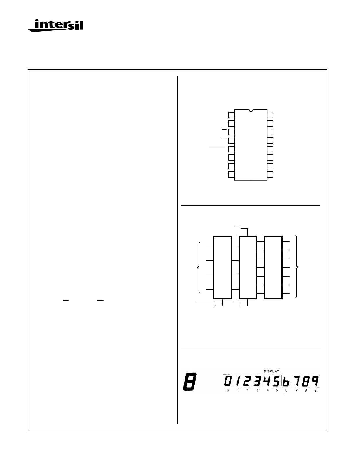
Pinout
CD4511BMS
TOP VIEW
1
B
2
C
3
LT
4
BL
VSS
5
D
6
A
7
8
/STROBE
LE
Functional Diagram
LT
7
A
1
B
BCD
INPUTS
C
D
LE/STROBE
VSS = 8
VDD = 16
L
A
T
C
2
H
6
5
BL
VDD
16
f
15
14
g
13
a
12
b
11
c
d
10
e
9
3
13
a
12
D
E
C
O
D
E
R
4
D
R
I
V
E
R
b
11
c
7
10
SEGMENT
d
OUTPUTS
9
e
15
f
14
g
These devices are similar to the type MC14511.
The CD4511BMS is supplied in these 16-lead outline
packages:
7-Segment Display
Braze Seal DIP H4W
Frit Seal DIP H2R
Ceramic Flatpack H6W
CAUTION: These devices are sensitive to electrostatic discharge; follow proper IC Handling Procedures.
1-888-INTERSIL or 321-724-7143 | Copyright © Intersil Corporation 1999
7-1169
a
g
b
f
e
c
d
File Number
3339
Specifications CD4511BMS
Absolute Maximum Ratings Reliability Information
DC Supply Voltage Range, (VDD) . . . . . . . . . . . . . . . -0.5V to +20V
(Voltage Referenced to VSS Terminals)
Input Voltage Range, All Inputs . . . . . . . . . . . . .-0.5V to VDD +0.5V
DC Input Current, Any One Input . . . . . . . . . . . . . . . . . . . . . . . .±10mA
Operating Temperature Range. . . . . . . . . . . . . . . . -55oC to +125oC
Package Types D, F, K, H
Storage Temperature Range (TSTG) . . . . . . . . . . . -65oC to +150oC
Lead Temperature (During Soldering) . . . . . . . . . . . . . . . . . +265oC
At Distance 1/16 ± 1/32 Inch (1.59mm ± 0.79mm) from case for
10s Maximum
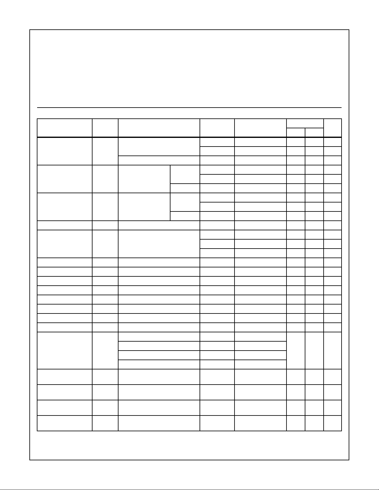
TABLE 1. DC ELECTRICAL PERFORMANCE CHARACTERISTICS
PARAMETER SYMBOL CONDITIONS (NOTE 1)
Supply Current IDD VDD = 20V, VIN = VDD or GND 1 +25oC-10µA
VDD = 18V, VIN = VDD or GND 3 -55oC-10µA
Input Leakage Current IIL VIN = VDD or GND VDD = 20 1 +25oC -100 - nA
VDD = 18V 3 -55oC -100 - nA
Input Leakage Current IIH VIN = VDD or GND VDD = 20 1 +25oC - 100 nA
VDD = 18V 3 -55oC - 100 nA
Output Voltage VOL15 VDD = 15V, No Load 1, 2, 3 +25oC, +125oC, -55oC - 50 mV
Output Voltage VOH15 VDD = 15V, No Load (Note 3) 1 +25oC 14.1 - V
Output Current (Sink) IOL5 VDD = 5V, VOUT = 0.4V 1 +25oC1-mA
Output Current (Sink) IOL10 VDD = 10V, VOUT = 0.5V 1 +25oC 2.6 - mA
Output Current (Sink) IOL15 VDD = 15V, VOUT = 1.5V 1 +25oC 6.8 - mA
Output Drive Voltage LVOH5 VDD = 5V, IOH = -20mA 1 +25oC 3.4 - V
Output Drive Voltage LVOH10 VDD = 10V, IOH = -20mA 1 +25oC 8.6 - V
Output Drive Voltage LVOH15 VDD = 15V, IOH = -20mA 1 +25oC 13.7 - V
N Threshold Voltage VNTH VDD = 10V, ISS = -10µA 1 +25oC -2.8 -0.7 V
P Threshold Voltage VPTH VSS = 0V, IDD = 10µA 1 +25oC 0.7 2.8 V
Functional F VDD = 2.8V, VIN = VDD or GND 7 +25oC VOH >
VDD = 20V, VIN = VDD or GND 7 +25oC
VDD = 18V, VIN = VDD or GND 8A +125oC
VDD = 3V, VIN = VDD or GND 8B -55oC
Input Voltage Low
(Note 2)
Input Voltage High
(Note 2)
Input Voltage Low
(Note 2)
Input Voltage High
(Note 2)
NOTES: 1. All voltages referenced to device GND, 100% testing being
implemented.
2. Go/No Go test with limits applied to inputs.
VIL VDD = 5V, VOH > 3.6V, VOL < 0.5V 1, 2, 3 +25oC, +125oC, -55oC - 1.5 V
VIH VDD = 5V, VOH > 3.6V, VOL < 0.5V 1, 2, 3 +25oC, +125oC, -55oC 3.5 - V
VIL VDD = 15V, VOH > 12.6V,
VOL < 1.5V
VIH VDD = 15V, VOH > 12.6V,
VOL < 1.5V
Thermal Resistance . . . . . . . . . . . . . . . . θ
Ceramic DIP and FRIT Package. . . . . 80oC/W 20oC/W
Flatpack Package . . . . . . . . . . . . . . . . 70oC/W 20oC/W
Maximum Package Power Dissipation (PD) at +125oC
For TA = -55oC to +100oC (Package Type D, F, K) . . . . . . 500mW
For TA = +100oC to +125oC (Package Type D, F, K). . . . . .Derate
Linearity at 12mW/oC to 200mW
Device Dissipation per Output Transistor . . . . . . . . . . . . . . . 100mW
For TA = Full Package Temperature Range (All Package Types)
Junction Temperature . . . . . . . . . . . . . . . . . . . . . . . . . . . . . . +175oC
GROUP A
SUBGROUPS TEMPERATURE
2 +125oC - 1000 µA
2 +125oC -1000 - nA
2 +125oC - 1000 nA
2 +125oC 14.2 V
3 -55oC 14.0 V
1, 2, 3 +25oC, +125oC, -55oC- 4 V
1, 2, 3 +25oC, +125oC, -55oC11 - V
3. For accuracy, voltage is measured differentially to VDD
ja
LIMITS
VDD/2
VOL <
VDD/2
θ
jc
UNITSMIN MAX
V
7-1170
Specifications CD4511BMS
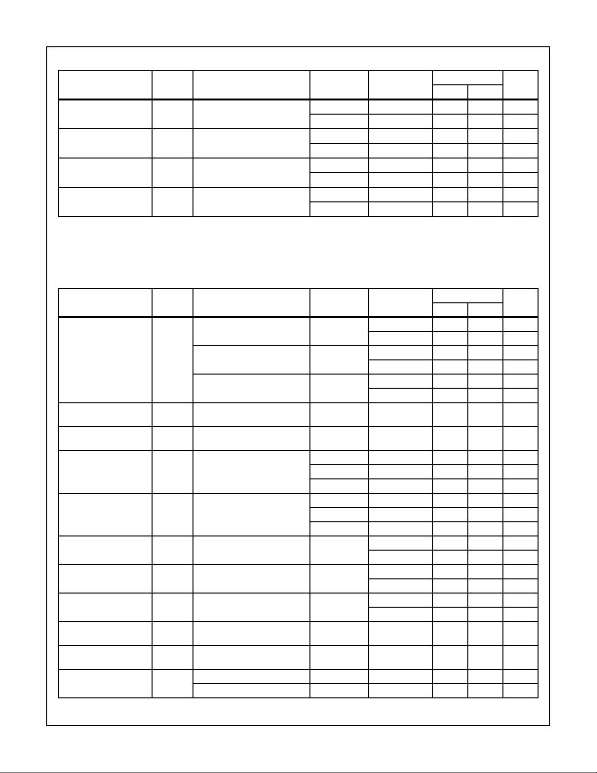
TABLE 2. AC ELECTRICAL PERFORMANCE CHARACTERISTICS
GROUP A
PARAMETER SYMBOL CONDITIONS (NOTE 1, 2)
Propagation Delay
Data to Output
Propagation Delay
Data to Output
Transition Time TTHL VDD = 5V, VIN = VDD or GND 9 +25oC - 310 ns
Transition Time TTLH VDD = 5V, VIN = VDD or GND 9 +25oC - 80 ns
NOTES:
1. CL = 50pF, RL = 200K, Input TR, TF < 20ns.
2. -55oC and +125oC limits guaranteed, 100% testing being implemented.
PARAMETER SYMBOL CONDITIONS NOTES TEMPERATURE
Supply Current IDD VDD = 5V, VIN = VDD or GND 1, 2 -55oC, +25oC- 5 µA
Output Voltage VOL VDD = 5V, No Load 1, 2 +25oC, +125oC,
Output Voltage VOL VDD = 10V, No Load 1, 2 +25oC, +125oC,
Output Voltage VOH VDD = 5V, No Load 1, 2 +25oC 4.1 - V
Output Voltage VOH VDD = 10V, No Load 1, 2 +25oC 9.1 - V
Output Current (Sink) IOL5 VDD = 5V, VOUT = 0.4V 1, 2 +125oC 0.36 - mA
Output Current (Sink) IOL10 VDD = 10V, VOUT = 0.5V 1, 2 +125oC 0.9 - mA
Output Current (Sink) IOL15 VDD = 15V, VOUT = 1.5V 1, 2 +125oC 2.4 - mA
Input Voltage Low VIL VDD = 10V, VOH > 9V , VOL < 1V 1, 2 +25oC, +125oC,
Input Voltage High VIH VDD = 10V, VOH > 9V, VOL < 1V 1, 2 +25oC, +125oC,
Propagation Delay
Data to Output
TPHL VDD = 5V, VIN = VDD or GND 9 +25oC - 1040 ns
TPLH VDD = 5V, VIN = VDD or GND 9 +25oC - 1320 ns
TABLE 3. ELECTRICAL PERFORMANCE CHARACTERISTICS
VDD = 10V, VIN = VDD or GND 1, 2 -55oC, +25oC- 10µA
VDD = 15V, VIN = VDD or GND 1, 2 -55oC, +25oC- 10µA
TPHL VDD = 10V 1, 2, 3 +25oC - 420 ns
VDD = 15V 1, 2, 3 +25oC - 300 ns
SUBGROUPS TEMPERATURE
10, 11 +125oC, -55oC - 1404 ns
10, 11 +125oC, -55oC - 1782 ns
10, 11 +125oC, -55oC - 419 ns
10, 11 +125oC, -55oC - 108 ns
+125oC - 150 µA
+125oC - 300 µA
+125oC - 600 µA
-55oC
-55oC
1, 2 +125oC 4.2 - V
1, 2 -55oC 4.0 - V
1, 2 +125oC 9.2 - V
1, 2 -55oC 9.0 - V
-55oC 0.64 - mA
-55oC 1.6 - mA
-55oC 4.2 - mA
-55oC
-55oC
LIMITS
UNITSMIN MAX
LIMITS
UNITSMIN MAX
-50mV
-50mV
-3V
+7 - V
7-1171
Specifications CD4511BMS
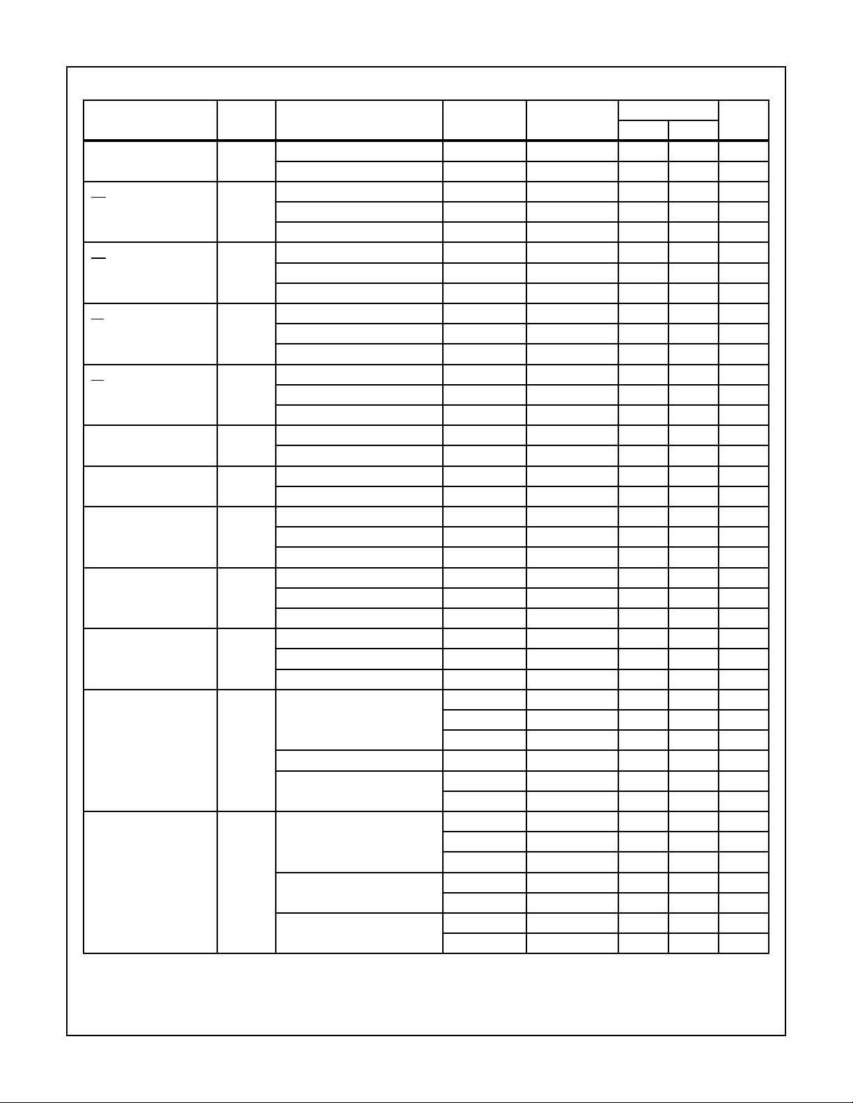
TABLE 3. ELECTRICAL PERFORMANCE CHARACTERISTICS(Continued)
LIMITS
PARAMETER SYMBOL CONDITIONS NOTES TEMPERATURE
Propagation Delay
Data to Output
Propagation Delay
(BT)
Propagation Delay
(BT)
Propagation Delay
(LT)
TPLH VDD = 10V 1, 2, 3 +25oC - 520 ns
VDD = 15V 1, 2, 3 +25oC - 360 ns
TPHL VDD = 5V 1, 2, 3 +25oC - 700 ns
o
VDD = 10V 1, 2, 3 +25
VDD = 15V 1, 2, 3 +25
C - 350 ns
o
C - 250 ns
TPLH VDD = 5V 1, 2, 3 +25oC - 800 ns
o
VDD = 10V 1, 2, 3 +25
VDD = 15V 1, 2, 3 +25
C - 350 ns
o
C - 300 ns
TPHL VDD = 5V 1, 2, 3 +25oC - 500 ns
VDD = 10V 1, 2, 3 +25oC - 250 ns
VDD = 15V 1, 2, 3 +25oC - 170 ns
Propagation Delay
(LT)
TPLH VDD = 5V 1, 2, 3 +25oC - 300 ns
VDD = 10V 1, 2, 3 +25oC - 150 ns
VDD = 15V 1, 2, 3 +25oC - 100 ns
Transition Time TTHL VDD = 10V 1, 2, 3 +25oC - 185 ns
VDD = 15V 1, 2, 3 +25oC - 160 ns
Transition Time TTLH VDD = 10V 1, 2, 3 +25oC - 60 ns
VDD = 15V 1, 2, 3 +25oC - 50 ns
Minimum Data Setup
Time
TS VDD = 5V 1, 2, 3 +25oC - 150 ns
VDD = 10V 1, 2, 3 +25oC - 70 ns
VDD = 15V 1, 2, 3 +25oC - 40 ns
Minimum Data Hold Time TH VDD = 5V 1, 2, 3 +25oC-0ns
VDD = 10V 1, 2, 3 +25oC-0ns
VDD = 15V 1, 2, 3 +25oC-0ns
Minimum Strobe Pulse
Width
TW VDD = 5V 1, 2, 3 +25oC - 400 ns
VDD = 10V 1, 2, 3 +25oC - 160 ns
VDD = 15V 1, 2, 3 +25oC - 100 ns
Output Drive Voltage LVOH5 VDD = 5V, IOH = -10mA 1, 2 +25oC 3.9 - V
1, 2 +125oC 3.9 - V
1, 2 -55oC 3.8 - V
VDD = 5V, IOH = -20mA 1, 2 -55oC 3.55 - V
VDD = 5V, IOH = -25mA 1, 2 +25oC 3.1 - V
1, 2 -55oC 3.4 - V
Output Drive Voltage LVOH10 VDD = 10V, IOH = -10mA 1, 2 +25oC 9.0 - V
1, 2 +125oC 9.0 - V
1, 2 -55oC 8.85 - V
VDD = 10V, IOH = -20mA 1, 2 +125oC 8.4 - V
1, 2 -55oC 8.7 - V
VDD = 10V, IOH = -25mA 1, 2 +25oC 8.3 - V
1, 2 -55oC 8.6 - V
UNITSMIN MAX
7-1172

Specifications CD4511BMS
TABLE 3. ELECTRICAL PERFORMANCE CHARACTERISTICS(Continued)
LIMITS
PARAMETER SYMBOL CONDITIONS NOTES TEMPERATURE
Output Drive Voltage LVOH15 VDD = 15V, IOH = -10mA 1, 2 +25oC 14.0 - V
1, 2 +125oC 14.0 - V
1, 2 -55oC 13.9 - V
o
VDD = 15V, IOH = -20mA 1, 2 +125
1, 2 -55
C 13.5 - V
o
C 13.75 - V
VDD = 15V, IOH = -25mA 1, 2 +25oC 13.5 - V
o
1, 2 -55
Input Capacitance CIN Any Input 1, 2 +25
C 13.65 - V
o
C - 7.5 pF
NOTES:
1. All voltages referenced to device GND.
2. The parameters listed on Table 3 are controlled via design or process and are not directly tested. These parameters are characterized
on initial design release and upon design changes which would affect these characteristics.
3. CL = 50pF, RL = 200K, Input TR, TF < 20ns.
TABLE 4. POST IRRADIATION ELECTRICAL PERFORMANCE CHARACTERISTICS
LIMITS
PARAMETER SYMBOL CONDITIONS NOTES TEMPERATURE
Supply Current IDD VDD = 20V, VIN = VDD or GND 1, 4 +25oC-25µA
N Threshold Voltage VNTH VDD = 10V, ISS = -10µA 1, 4 +25oC -2.8 -0.2 V
N Threshold Voltage
∆VTN VDD = 10V, ISS = -10µA 1, 4 +25oC-±1V
Delta
P Threshold Voltage VTP VSS = 0V, IDD = 10µA 1, 4 +25oC 0.2 2.8 V
P Threshold Voltage
∆VTP VSS = 0V, IDD = 10µA 1, 4 +25oC-±1V
Delta
Functional F VDD = 18V, VIN = VDD or GND 1 +25oC VOH >
VDD/2
Propagation Delay Time TPHL
VDD = 3V, VIN = VDD or GND
VDD = 5V 1, 2, 3, 4 +25oC - 1.35 x
TPLH
VOL <
VDD/2
+25oC
Limit
NOTES: 1. All voltages referenced to device GND.
2. CL = 50pF, RL = 200K, Input TR, TF < 20ns.
3. See Table 2 for +25oC limit.
4. Read and Record
UNITSMIN MAX
UNITSMIN MAX
V
ns
TABLE 5. BURN-IN AND LIFE TEST DELTA PARAMETERS +25oC
PARAMETER SYMBOL DELTA LIMIT
Supply Current - MSI-2 IDD ± 1.0µA
Output Current (Sink) IOL5 ± 20% x Pre-Test Reading
Output Current (Source) IOH5A ± 20% x Pre-Test Reading
TABLE 6. APPLICABLE SUBGROUPS
MIL-STD-883
CONFORMANCE GROUP
METHOD GROUP A SUBGROUPS READ AND RECORD
Initial Test (Pre Burn-In) 100% 5004 1, 7, 9 IDD, IOL5, IOH5A
Interim Test 1 (Post Burn-In) 100% 5004 1, 7, 9 IDD, IOL5, IOH5A
Interim Test 2 (Post Burn-In) 100% 5004 1, 7, 9 IDD, IOL5, IOH5A
7-1173

Specifications CD4511BMS
TABLE 6. APPLICABLE SUBGROUPS (Continued)
MIL-STD-883
CONFORMANCE GROUP
PDA (Note 1) 100% 5004 1, 7, 9, Deltas
Interim Test 3 (Post Burn-In) 100% 5004 1, 7, 9 IDD, IOL5, IOH5A
PDA (Note 1) 100% 5004 1, 7, 9, Deltas
Final Test 100% 5004 2, 3, 8A, 8B, 10, 11
Group A Sample 5005 1, 2, 3, 7, 8A, 8B, 9, 10, 11
Group B Subgroup B-5 Sample 5005 1, 2, 3, 7, 8A, 8B, 9, 10, 11, Deltas Subgroups 1, 2, 3, 9, 10, 11
Subgroup B-6 Sample 5005 1, 7, 9
Group D Sample 5005 1, 2, 3, 8A, 8B, 9 Subgroups 1, 2 3
NOTE: 1. 5% Parameteric, 3% Functional; Cumulative for Static 1 and 2.
CONFORMANCE GROUPS
Group E Subgroup 2 5005 1, 7, 9 Table 4 1, 9 Table 4
METHOD GROUP A SUBGROUPS READ AND RECORD
TABLE 7. TOTAL DOSE IRRADIATION
MIL-STD-883
METHOD
PRE-IRRAD POST-IRRAD PRE-IRRAD POST-IRRAD
TEST READ AND RECORD
TABLE 8. BURN-IN AND IRRADIATION TEST CONNECTIONS
OSCILLATOR
FUNCTION OPEN GROUND VDD 9V ± -0.5V
Static Burn-In 1
(Note 1)
Static Burn-In 2
(Note 1)
Dynamic BurnIn (Note 1)
Irradiation
(Note 2)
NOTES:
1. Each pin except VDD and GND will have a series resistor of 10K ± 5%, VDD = 18V ± 0.5V
2. Each pin except VDD and GND will have a series resistor of 47K ± 5%; Group E, Subgroup 2, sample size is 4 dice/wafer, 0 failures,
VDD = 10V ± 0.5V
9-15 1-8 16
9-15 8 1-7, 16
9-15 5, 8 3, 4, 16 - 1, 2, 7 6
9-15 8 1-7, 16
50kHz 25kHz
7-1174

Logic Diagram
CD4511BMS
VDD
(BL)
P
TG
N
*
A
*
B
*
C
P
TG
N
P
TG
N
P
TG
N
P
TG
N
P
TG
N
P
TG
N
*
DRIVER
LOGIC
VSS
IOH
VOH
OUTPUT
DRIVERS
+
-
a
b
c
d
e
f
TG
P
N
g
STROBE
LE/
*
D
*
*
LT
ALL INPUTS ARE PROTECTED
*
BY CMOS PROTECTION NETWORK
FIGURE 1.
TRUTH TABLE
LE BI LTDCBAabcdefgDISPLAY
XX0XXXX1111111
X01XXXX0000000 Blank
01100001111110
01100010110000
01100101101101
01100111111001
VDD
VSS
01101000110011
01101011011011
7-1175

CD4511BMS
TRUTH TABLE (Continued)
LE BI LTDCBAabcdefgDISPLAY
01101100011111
01101111110000
01110001111111
01110011110011
01110100000000 Blank
01110110000000 Blank
01111000000000 Blank
01111010000000 Blank
01111100000000 Blank
01111110000000 Blank
111XXXX * *
X = Don’t Care
* Depends on BCD code previously applied when LE = 0
NOTE: Display is blank for all illegal input codes (BCD > 1001).
Typical Performance Characteristics
AMBIENT TEMPERATURE (TA) = +25oC
30
25
20
15
10
5
OUTPUT LOW (SINK) CURRENT (IOL) (mA)
0 5 10 15
FIGURE 2. TYPICAL OUTPUT LOW (SINK) CURRENT
GATE-TO-SOURCE VOLTAGE (VGS) = 15V
10V
5V
DRAIN-TO-SOURCE VOLTAGE (VDS) (V)
CHARACTERISTICS
700
600
500
400
300
200
100
PROPAGATION DELAY TIME (tPLH) (ns)
0 25 50 75 100
AMBIENT TEMPERATURE (TA) = +25oC
LOAD CAPACITANCE (CL) (pF)
SUPPLY VOLTAGE (VDD) = 5V
10V
15V
FIGURE 3. TYPICAL DATA-T O-OUTPUT , LOW -TO-HIGH-LEVEL
PROPAGATION DELAY TIME AS A FUNCTION OF
LOAD CAPACITANCE
7-1176

Typical Performance Characteristics
700
AMBIENT TEMPERATURE (TA) = +25oC
600
500
SUPPLY VOLTAGE (VDD) = 5V
CD4511BMS
AMBIENT TEMPERATURE (TA) = +25oC
60
SUPPLY VOLTAGE (VDD) = 5V
50
400
300
10V
200
100
15V
PROPAGATION DELAY TIME (tPLH) (ns)
0 25 50 75 100
LOAD CAPACITANCE (CL) (pF)
FIGURE 4. TYPICAL DATA-T O-OUTPUT , HIGH-T O-LOW-LEVEL
PROPAGATION DELAY TIME AS A FUNCTION OF
LOAD CAPACITANCE
AMBIENT TEMPERATURE (TA) = +25oC
500
400
300
200
TRANSITION TIME (tTHL) (ns)
100
SUPPLY VOLTAGE (VDD) = 5V
10V
15V
40
30
10V
15V
20
TRANSITION TIME (tTLH) (ns)
10
0
25 50 75 100
LOAD CAPACITANCE (CL) (pF)
FIGURE 5. TYPICAL LOW-TO-HIGH-LEVEL TRANSITION TIME
AS A FUNCTION OF LOAD CAPACITANCE
AMBIENT TEMPERATURE (TA) = +25oC
25
SUPPLY VOLTAGE (VDD) = 15V
20
15
10
5
OUTPUT SOURCE CURRENT (IOH) (mA)
10V
5V
0
100 200 300 400 500
LOAD CAPACITANCE (CL) (pF)
FIGURE 6. TYPICAL HIGH-TO-LOW TRANSITION TIME AS A
FUNCTION OF LOAD CAPACITANCE
5
10
8
6
AMBIENT TEMPERATURE (TA) = +25oC
4
2
4
10
8
6
4
SUPPLY VOLTS (VDD) = 15V
2
3
10
8
6
4
2
2
10
8
6
4
2
1
10
8
6
4
2
DYNAMIC POWER DISSIPATION (PD) (µW)
0
10
10
8642
-2
-1
10
FREQUENCY (f) (kHz)
FIGURE 8. TYPICAL DYNAMIC POWER DISSIPATION CHARACTERISTICS
0 0.5 1 1.5
SUPPLY VOLTAGE - OUTPUT DRIVE VOLTAGE (VDD - VOH) (V)
FIGURE 7. TYPICAL VOLT AGE DROP (VDD TO OUTPUT) vs OUT-
PUT SOURCE CURRENT AS A FUNCTION OF SUPPL Y
10V
10V
5V
CL = 50pF
CL = 15pF
8642
10
8642
0
10
8642
1
2
10
8642
3
10
7-1177

Applications Interfacing with Various Displays
CD4511BMS
A
B
BCD
INPUTS
DUTY CYCLE = 100%
ISEG = IDIODEAVG. =
VOH - VDF
R =
C
D
LE
BL
TO VDD
ISEG
VDD
LT
LATCH
8
DECODER
CD4511BMS
20mA AT LUMINOUS INTENSITY/SEGMENT = 250µcd
VSS
VDD
VDD
VSS
+
VOH
-
e
g
ISEG
Ra
Rb
Rc
Rd
R
Rf
R
LED 7-SEGMENT
DISPLAY
VDF
+
-
FIGURE 9. DRIVING COMMON CATHODE 7-SEGMENT LED DISPLAYS (EXAMPLE HEWLET-PACKARD 5082-7740)
LT
A
B
C
D
VDD
a
b
c
d
e
f
LE
BL
VDD
A MEDIUM BRIGHTNESS INTENSITY DISPLAY CAN BE OBTAINED WITH
LOW VOLTAGE FLUORESCENT DISPLAYS SUCH AS THE TUNG-SOL
DIGIVAC S/G* SERIES
* Trademark Tung-Sol Division Wagner Electric Co.
CD4511BMS
VSS
g
1.6V
AC OR DC
LT
A
B
C
D
LE
VDD
BL
2 OF 7 SEGMENTS SHOWN CONNECTED
RESISTORS R FROM VDD TO EACH 7-SEGMENT DRIVER OUTPUT ARE
CHOSEN TO KEEP ALL NUMITRON SEGMENTS SLIGHTL Y ON AND WARM
CD4511BMS
VSS
VDD = 5V
a
b
c
d
e
f
g
VDD
R ≈
400Ω
VDD
R ≈ 400Ω
FIGURE 10. DRIVING LOW VOLTAGE FLOURESCENT DISPLAYS FIGURE 11. DRIVING INCANDESCENT DISPLAYS (RCA NU-
MITRON DR2000 SERIES DISPLAYS)
All Intersil semiconductor products are manufactured, assembled and tested under ISO9000 quality systems certification.
Intersil products are sold by description only. Intersil Corporation reserves the right to make changes in circuit design and/or specifications at any time without
notice. Accordingly, the reader is cautioned to verify that data sheets are current before placing orders. Information furnished by Intersil is believed to be accurate
and reliable. However, no responsibility is assumed by Intersil or its subsidiaries for its use; nor for any infringements of patents or other rights of third parties which
may result from its use. No license is granted by implication or otherwise under any patent or patent rights of Intersil or its subsidiaries.
For information regarding Intersil Corporation and its products, see web site http://www.intersil.com
1178

CD4511BMS
Applications
MULTIPLEXING SCHEME SHOWING
2 OF 7 SEGMENTS CONNECTED
TRANSISTORS T1 - T4 (2N3053 OR 2N2102)
HAVE IC MAX. RATING > 7 x ISEG
DUTY CYCLE = 25%
ISEG = (IDIODEAVG) x 4
(VOH - VDF-VCE)
R =
ISEG
Interfacing with Various Displays (Continued)
CD4511BMS
Q0
Q1
Q2
Q3
VDD
a
b
c
d
e
f
g
+
-
R
R
VOH
5
6
7
1
CD4024BMS
2
VO1
V02
VO3
LT
A
B
C
D
LE
VDD
BL
2 4
12
311
CD4555BMS
1
9
VSS
VSS
ISEG
+
VDF
-
T1
VSS
+
VCE
T2
VSS
T3
VSS
T4
VSS
FIGURE 12. MULTIPLEXING WITH COMMON CATHODE 7-SEGMENT LED DISPLAYS (EXAMPLE HEWLET-PACKARD 5082-7404
4 CHARACTER DISPLAY OR 4 DISCRETE MONOSANTO MAN 3 DISPLAYS)
Waveforms
20ns
20ns
10%
50%
90%
50%
10%
20ns
10%
tSU
90%
tW
50%
90%
VDD
tHOLD
50%
20ns
VDD
0
VDD
0
FOR SETUP
FOR HOLD
0
OUTPUT
tr, tf = 20ns
DATA
INPUT
tPHL
tr tf
VDD
90%
50%
10%
tTLHtTHL
90%
50%
10%
tPLH
0
VDD
0
LE
DATA
INPUTS
OUTPUT
STROBE
tr, tf = 20ns
FIGURE 13. DYNAMIC WAVEFORMS
Chip Dimensions and Pad Layout
7-1179
Dimensions in parenthesis are in millimeters and are
derived from the basic inch dimensions as indicated.
Grid graduations are in mils (10
-3
inch).
METALLIZATION: Thickness: 11kÅ − 14kÅ, AL.
PASSIVATION: 10.4kÅ - 15.6kÅ, Silane
BOND PADS: 0.004 inches X 0.004 inches MIN
DIE THICKNESS: 0.0198 inches - 0.0218 inches
 Loading...