Intersil Corporation CD4097BMS, CD4067BMS Datasheet

December 1992
CD4067BMS
CD4097BMS
CMOS Analog
Multiplexers/Demultiplexers
Features
• High Voltage Types (20V Rating)
• CD4067BMS Single 16 Channel Multiplexer/Demultiplexer
• CD4097BMS Differential 8 Channel Multiplexer/Demultiplexer
• Low ON Resistance: 125Ω (typ) Over 15Vp-p Signal
Input Range for VDD - VSS = 15V
• High OFF Resistance: Channel Leakage of ±10pA (typ)
at VDD - VSS = 18V
• Matched Switch Characteristics: RON = 5Ω (typ) for
VDD - VSS = 15V
• Very Low Quiescent Power Dissipation Under All Digital Control Input and Supply Conditions: 0.2µW (typ)
at VDD - VSS = 10V
• Binary Address Decoding on Chip
• 5V, 10V and 15V Parametric Ratings
• 100% Tested for Quiescent Current at 20V
• Maximum Input Current of 1µA at 18V Over Full Package Temperature Range; 100nA at 18V and +25
o
C
• Standardized Symmetrical Output Characteristics
Applications
• Analog and Digital Multiplexing and Demultiplexing
• A/D and D/A Conversion
• Signal Gating
* When these devices are used as demultiplexers the “CHANNEL
IN/OUT” terminals are the outputs and the “COMMON OUT/IN” terminals are the inputs.
Description
CD4067BMS and CD4097BMS CMOS analog multiplexers/
demultiplexers* are digitally controlled analog switches having
low ON Impedance, low OFF leakage current, and internal
address decoding. In addition, the ON resistance is relatively
constant over the full input-signal range.
The CD4067BMS is a 16 channel multiplexer with four binary
control inputs, A, B, C, D and an inhibit input, arranged so that
any combination of the inputs selects one switch.
The CD4097BMS is a differential 8 channel multiplexer having
three binary control inputs A, B, C and an inhibit input. The inputs
permit selection of one of eight pairs of switches. A logic “1”
present at the inhibit input turns all channels off.
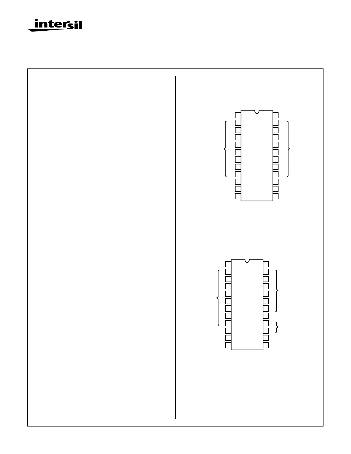
The CD4067BMS and CD4097BMS are supplied in these 24
lead outline packages:
Braze Seal DIP *H4V †H6M
Frit Seal DIP *H1Z †HFN
Ceramic Flatpack *H4P †H4P
*CD4067B Only †CD4097B
Pinout
CHANNEL X
COMMON OUT/IN
*
CHANNEL
*
IN/OUT
COMMON X
IN/OUT
OUT/IN
VSS
VSS
1
2
7
3
6
4
5
5
4
6
3
7
2
8
1
0
9
A
10
B
11
12
CD4067BMS
TOP VIEW
1
2
7
3
6
4
5
5
4
6
3
7
2
8
1
9
0
10
A
11
B
12
CD4097BMS
TOP VIEW
24
23
22
21
20
19
18
17
16
15
14
13
24
VDD
0
23
1
22
21
2
3
20
19
4
5
18
COMMON Y
17
OUT/IN
6
16
7
15
C
14
INHIBIT
13
VDD
8
9
10
11
*
12
13
14
15
INHIBIT
C
D
Y CHANNEL
IN/OUT
Y CHANNEL
IN/OUT
CAUTION: These devices are sensitive to electrostatic discharge; follow proper IC Handling Procedures.
1-888-INTERSIL or 321-724-7143 | Copyright © Intersil Corporation 1999
7-1
File Number 3190

Specifications CD4067BMS, CD4097BMS
Absolute Maximum Ratings Reliability Information
DC Supply Voltage Range, (VDD) . . . . . . . . . . . . . . . -0.5V to +20V
(Voltage Referenced to VSS Terminals)
Input Voltage Range, All Inputs . . . . . . . . . . . . .-0.5V to VDD +0.5V
DC Input Current, Any One Input . . . . . . . . . . . . . . . . . . . . . . . .±10mA
Operating Temperature Range. . . . . . . . . . . . . . . . -55
Package Types D, F, K, H
Storage Temperature Range (TSTG) . . . . . . . . . . . -65
o
C to +125oC
o
C to +150oC
Lead Temperature (During Soldering) . . . . . . . . . . . . . . . . . +265
At Distance 1/16 ± 1/32 Inch (1.59mm ± 0.79mm) from case for
10s Maximum
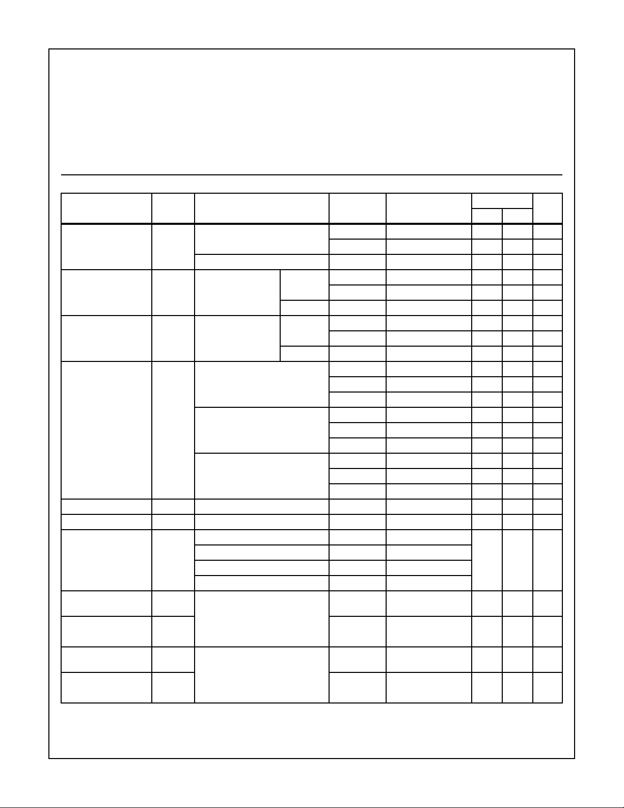
TABLE 1. DC ELECTRICAL PERFORMANCE CHARACTERISTICS
PARAMETER SYMBOL CONDITIONS (NOTE 1)
Supply Current IDD VDD = 20V, VIN = VDD or GND 1 +25
VDD = 18V, VIN = VDD or GND 3 -55oC-10µA
Input Leakage Current IIL VIN = VDD or GND VDD = 20 1 +25
VDD = 18V 3 -55oC -100 - nA
Input Leakage Current IIH VIN = VDD or GND VDD = 20 1 +25oC - 100 nA
VDD = 18V 3 -55oC - 100 nA
ON-State Resistance
RL = 10K Returned to
RON VDD = 5V
VIS = VSS to VDD
VDD - VSS/2
VDD = 10V
VIS = VSS to VDD
VDD = 15V
VIS = VSS to VDD
N Threshold Voltage VNTH VDD = 10V, ISS = -10µA 1 +25oC -2.8 -0.7 V
P Threshold Voltage VPTH VSS = 0V, IDD = 10µA 1 +25oC 0.7 2.8 V
Functional (Note 4) F VDD = 2.8V, VIN = VDD or GND 7 +25oC VOH >
VDD = 20V, VIN = VDD or GND 7 +25oC
VDD = 18V, VIN = VDD or GND 8A +125oC
VDD = 3V, VIN = VDD or GND 8B -55oC
Input Voltage Low
(Note 2)
Input Voltage High
(Note 2)
Input Voltage Low
(Note 2)
Input Voltage High
(Note 2)
VIL VDD = 5V = VIS Thru 1K
VEE = VSS
RL = 1K to VSS
VIH 1, 2, 3 +25oC, +125oC, -55oC 3.5 - V
|ISS| < 2µA on all
OFF Channels
VIL VDD = 15V = VIS Thru 1K
VEE = VSS
RL = 1K to VSS
VIH 1, 2, 3 +25oC, +125oC, -55oC11 - V
|ISS| < 2µA on all
OFF Channels
Thermal Resistance . . . . . . . . . . . . . . . . θ
Ceramic DIP and FRIT Package. . . . . 80oC/W 20oC/W
Flatpack Package . . . . . . . . . . . . . . . . 70
Maximum Package Power Dissipation (PD) at +125oC
For TA = -55
For TA = +100
o
C
Device Dissipation per Output Transistor . . . . . . . . . . . . . . . 100mW
o
C to +100oC (Package Type D, F, K). . . . . . 500mW
o
C to +125oC (Package Type D, F, K) . . . . .Derate
Linearity at 12mW/oC to 200mW
ja
o
C/W 20oC/W
For TA = Full Package Temperature Range (All Package Types)
Junction Temperature . . . . . . . . . . . . . . . . . . . . . . . . . . . . . . +175oC
GROUP A
LIMITS
SUBGROUPS TEMPERATURE
o
C-10µA
2 +125oC - 1000 µA
o
C -100 - nA
2 +125oC -1000 - nA
2 +125oC - 1000 nA
1 +25oC - 1050 Ω
2 +125oC - 1300 Ω
3 -55oC - 800 Ω
1 +25oC - 400 Ω
2 +125oC - 500 Ω
3 -55oC - 310 Ω
1 +25oC - 240 Ω
2 +125oC - 320 Ω
3 -55oC - 220 Ω
VOL <
VDD/2
VDD/2
1, 2, 3 +25oC, +125oC, -55oC - 1.5 V
1, 2, 3 +25oC, +125oC, -55oC- 4 V
θ
jc
UNITSMIN MAX
V
7-2

Specifications CD4067BMS, CD4097BMS
TABLE 1. DC ELECTRICAL PERFORMANCE CHARACTERISTICS
PARAMETER SYMBOL CONDITIONS (NOTE 1)
OFF Channel Leakage
Any Channel OFF or All
Channels OFF
(Common OUT/IN)
NOTES: 1. All voltages referenced to device GND, 100% testing being
implemented.
2. Go/No Go test with limits applied to inputs.
PARAMETER SYMBOL CONDITIONS
Propagation Delay
(Signal In to Output)
Propagation Delay
Address or Inhibit to
Signal Out.
(Channel Turning On)
NOTES:
1. CL = 50pF, RL = 200K, Input TR, TF < 20ns.
2. -55oC and +125oC limits guaranteed, 100% testing being implemented.
3. CL = 50pF, RL = 10K, Input TR, TF < 20ns.
IOZL VOUT = 0V VDD = 20V 1 +25oC -0.1 - µA
VDD = 18V 3 -55oC -0.1 - µA
IOZH VOUT = VDD VDD = 20V 1 +25oC - 0.1 µA
VDD = 18V 3 -55oC - 0.1 µA
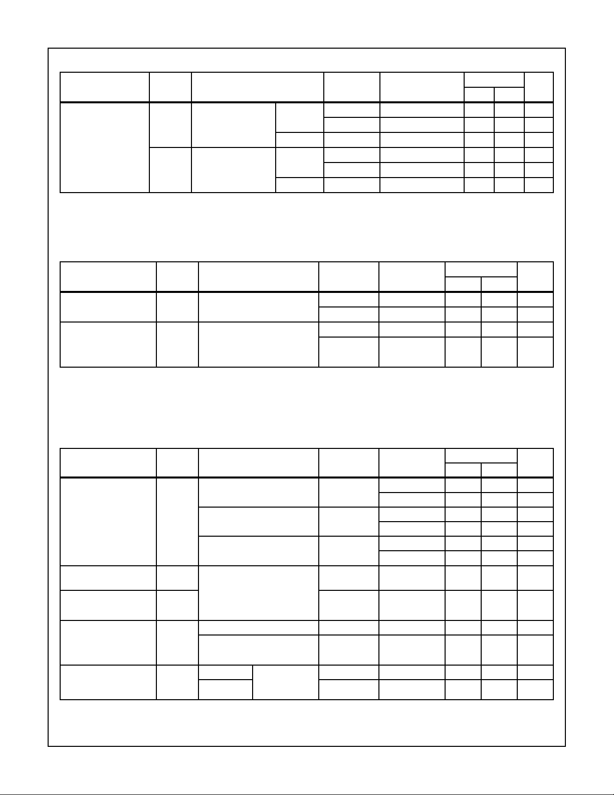
TABLE 2. AC ELECTRICAL PERFORMANCE CHARACTERISTICS
TPHL
TPLH
TPZH
TPZL
VDD = 5V, VIN = VDD or GND
(Notes 1, 2)
VDD = 5V, VIN = VDD or GND
(Notes 2, 3)
GROUP A
SUBGROUPS TEMPERATURE
2 +125oC -1.0 - µA
2 +125oC - 1.0 µA
3. For accuracy, voltage is measured differentially to VDD. Limit
is 0.050V max.
4. VDD = 2.8/3.0V, RL = 200K
VDD = 20V/18V, RL = 10K - 25K
GROUP A
SUBGROUPS TEMPERATURE
9 +25oC - 60 ns
10, 11 +125oC, -55oC - 81 ns
9 +25oC - 650 ns
10, 11 +125oC, -55oC - 878 ns
LIMITS
UNITSMIN MAX
LIMITS
UNITSMIN MAX
TABLE 3. ELECTRICAL PERFORMANCE CHARACTERISTICS
LIMITS
PARAMETER SYMBOL CONDITIONS NOTES TEMPERATURE
Supply Current IDD VDD = 5V, VIN = VDD or GND 1, 2 -55oC, +25oC- 5 µA
+125oC - 150 µA
VDD = 10V, VIN = VDD or GND 1, 2 -55oC, +25oC- 10µA
+125oC - 300 µA
VDD = 15V, VIN = VDD or GND 1, 2 -55oC, +25oC- 10µA
+125oC - 600 µA
Input Voltage Low VIL VDD = VIS = 10V
VEE = VSS
Input Voltage High VIH 1, 2 +25oC, +125oC,
Propagation Delay
Address or Inhibit to
Signal Out.
(Channel Turning On)
Propagation Delay
Signal In to Output
TPZH
TPZL
TPHL
TPLH
RL = 1K to VSS
IIS < 2µA
ON OFF Channel
VDD = 10V 1, 2, 4 +25oC - 270 ns
VDD = 15V 1, 2, 4 +25oC - 190 ns
VDD = 10V VIS = VDD or
VDD = 15V 1, 2, 3 +25oC - 20 ns
GND
1, 2 +25oC, +125oC,
-55oC
-55oC
1, 2, 3 +25oC - 30 ns
-3V
+7 - V
UNITSMIN MAX
7-3
 Loading...