Intersil Corporation CD4089BMS Datasheet

CD4089BMS
December 1992
Features
• High Voltage Type (20V Rating)
• Cascadable in Multiples of 4 Bits
• Set to “15” Input and “15” Detect Output
• 100% Tested for Quiescent Current at 20V
• 5V, 10V and 15V Parametric Ratings
• Standardized Symmetrical Output Characteristics
• Maximum Input Current of 1µA at 18V Over Full Pack-
age Temperature Range; 100nA at 18V and +25
• Noise Margin (Over Full Package/Temperature Range)
- 1V at VDD = 5V
- 2V at VDD = 10V
- 2.5V at VDD = 15V
• Meets All Requirements of JEDEC Tentative Standard
No. 13B, “Standard Specifications for Description of
‘B’ Series CMOS Devices”
Applications
• Numerical Control
• Instrumentation
• Digital Filtering
• Frequency Synthesis
Description
CD4089BMS is a low power 4 bit digital rate multiplier that
provides an output pulse rate that is the clock-input-pulse
rate multiplied by
when the binary input number is 13, there will be 13 output
pulses for every 16 input pulses. This device may be used in
1
/16 times the binary input. For example,
CMOS Binary Rate Multiplier
conjunction with an up/down counter and control logic used
to perform arithmetic operations (adds, subtract, divide, raise
to a power), solve algebraic and differential equations,
generate natural logarithms and trigometric functions, A/D
and D/A conversions, and frequency division.
For words of more than 4 bits, CD4089BMS devices may be
cascaded in two different modes: an Add mode and a Multiply mode (see Figures 3 and 4). In the Add mode some of
the gaps left by the more significant unit at the count of 15
are filled in by the less significant units. For example, when
o
C
two units are cascaded in the Add mode and programmed to
11 and 13, respectively, the more significant unit will have 1 1
output pulses for every 16 input pulses and the other unit will
have 13 output pulses for every 256 input pulses for a total of
11
16 256 256
13
+
189
=
In the Multiply mode the fraction programmed into the first
rate multiplier is multiplied by the fraction programmed into
the second multiplier. Thus the output rate will be
11
13
x
16 16 256
143
=
The CD4089BMS has an internal synchronous 4 bit counter
which, together with one of the four binary input bits, produces pulse trains as shown in Figure 6.
If more than one binary input bit is high, the resulting pulse
train is a combination of the separate pulse trains as shown
in Figure 6.
The CD4089BMS is supplied in these 16-lead outline packages:
Braze Seal DIP H4W
Frit Seal DIP H2R
Ceramic Flatpack H6P
Pinout
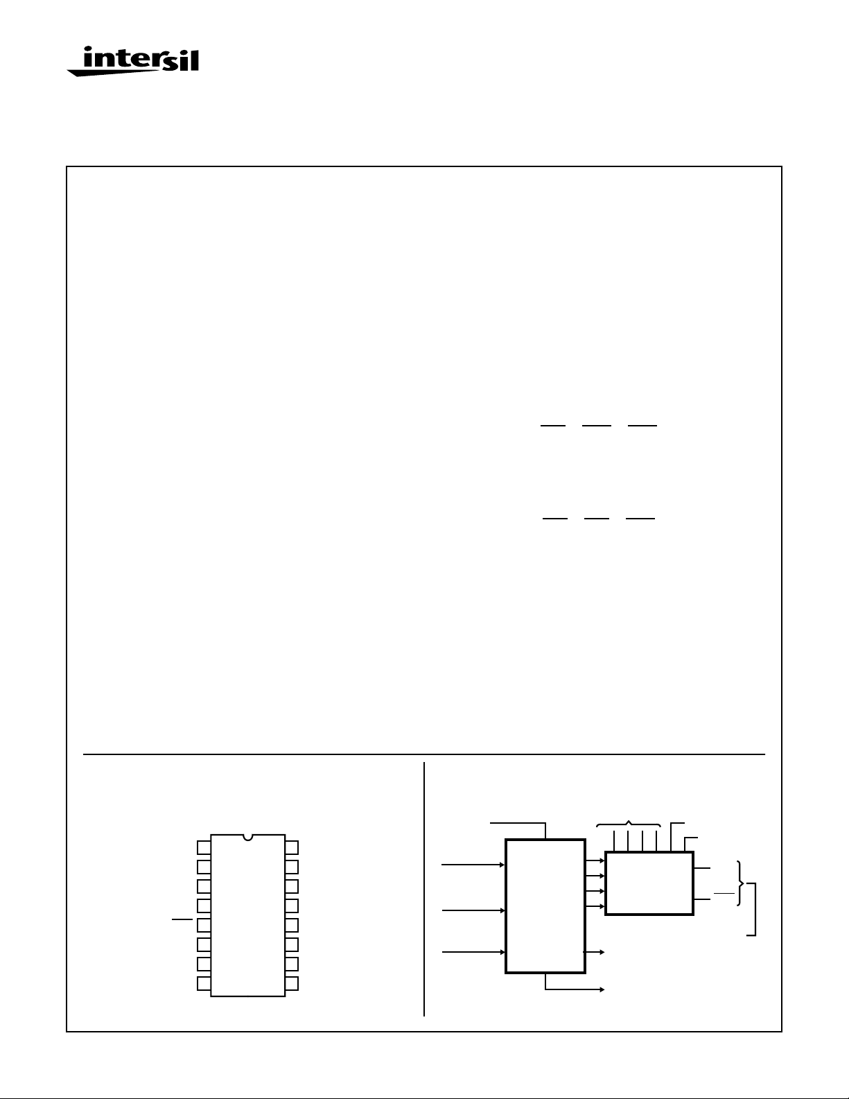
CD4089BMS
TOP VIEW
16
VDD
15
B
14
A
13
CLEAR
12
CASCADE
11
INHIBIT IN (CARRY)
10
STROBE
9
CLOCK
OUT
OUT
VSS
1
2
C
3
D
4
5
6
7
8
“15” OUT
SET TO “15”
INHIBIT OUT (CARRY)
CAUTION: These devices are sensitive to electrostatic discharge; follow proper IC Handling Procedures.
1-888-INTERSIL or 321-724-7143 | Copyright © Intersil Corporation 1999
Functional Diagram
CLOCK
INHIBIT
(CARRY) IN
11
SET TO
“15”
4
CLEAR
13
VDD = 16
VSS = 8
7-1064
9
4 BIT
BINARY
COUNTER
7
BINARY RATE
SELECT INPUTS
A
14B15C2D3
RATE
SELECT
LOGIC
“15” OUT
1
INHIBIT (CARRY) OUT
STROBE
10
CASCADE
12
OUT
6
OUT
5
RATE
OUTPUTS
File Number
3329

Specifications CD4089BMS
Absolute Maximum Ratings Reliability Information
DC Supply Voltage Range, (VDD) . . . . . . . . . . . . . . . -0.5V to +20V
(Voltage Referenced to VSS Terminals)
Input Voltage Range, All Inputs . . . . . . . . . . . . .-0.5V to VDD +0.5V
DC Input Current, Any One Input . . . . . . . . . . . . . . . . . . . . . . . .±10mA
Operating Temperature Range. . . . . . . . . . . . . . . . -55
Package Types D, F, K, H
Storage Temperature Range (TSTG) . . . . . . . . . . . -65
o
C to +125oC
o
C to +150oC
Lead Temperature (During Soldering) . . . . . . . . . . . . . . . . . +265
At Distance 1/16 ± 1/32 Inch (1.59mm ± 0.79mm) from case for
10s Maximum
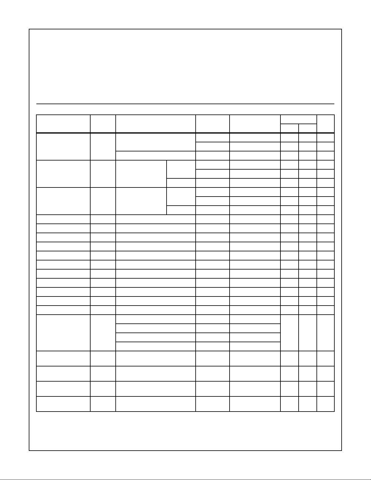
TABLE 1. DC ELECTRICAL PERFORMANCE CHARACTERISTICS
PARAMETER SYMBOL CONDITIONS (NOTE 1)
Supply Current IDD VDD = 20V, VIN = VDD or GND 1 +25
VDD = 18V, VIN = VDD or GND 3 -55oC-10µA
Input Leakage Current IIL VIN = VDD or GND VDD = 20 1 +25
VDD = 18V 3 -55oC -100 - nA
Input Leakage Current IIH VIN = VDD or GND VDD = 20 1 +25oC - 100 nA
VDD = 18V 3 -55oC - 100 nA
Output Voltage VOL15 VDD = 15V, No Load 1, 2, 3 +25oC, +125oC, -55oC - 50 mV
Output Voltage VOH15 VDD = 15V, No Load (Note 3) 1, 2, 3 +25oC, +125oC, -55oC 14.95 - V
Output Current (Sink) IOL5 VDD = 5V, VOUT = 0.4V 1 +25oC 0.53 - mA
Output Current (Sink) IOL10 VDD = 10V, VOUT = 0.5V 1 +25oC 1.4 - mA
Output Current (Sink) IOL15 VDD = 15V, VOUT = 1.5V 1 +25oC 3.5 - mA
Output Current (Source) IOH5A VDD = 5V, VOUT = 4.6V 1 +25oC - -0.53 mA
Output Current (Source) IOH5B VDD = 5V, VOUT = 2.5V 1 +25oC - -1.8 mA
Output Current (Source) IOH10 VDD = 10V, VOUT = 9.5V 1 +25oC - -1.4 mA
Output Current (Source) IOH15 VDD = 15V, VOUT = 13.5V 1 +25oC - -3.5 mA
N Threshold Voltage VNTH VDD = 10V, ISS = -10µA 1 +25oC -2.8 -0.7 V
P Threshold Voltage VPTH VSS = 0V, IDD = 10µA 1 +25oC 0.7 2.8 V
Functional F VDD = 2.8V, VIN = VDD or GND 7 +25oC VOH >
VDD = 20V, VIN = VDD or GND 7 +25oC
VDD = 18V, VIN = VDD or GND 8A +125oC
VDD = 3V, VIN = VDD or GND 8B -55oC
Input Voltage Low
VIL VDD = 5V, VOH > 4.5V, VOL < 0.5V 1, 2, 3 +25oC, +125oC, -55oC - 1.5 V
(Note 2)
Input Voltage High
VIH VDD = 5V, VOH > 4.5V, VOL < 0.5V 1, 2, 3 +25oC, +125oC, -55oC 3.5 - V
(Note 2)
Input Voltage Low
(Note 2)
Input Voltage High
(Note 2)
VIL VDD = 15V, VOH > 13.5V,
VOL < 1.5V
VIH VDD = 15V, VOH > 13.5V,
VOL < 1.5V
NOTES: 1. All voltages referenced to device GND, 100% testing being
implemented.
2. Go/No Go test with limits applied to inputs.
Thermal Resistance . . . . . . . . . . . . . . . . θ
Ceramic DIP and FRIT Package. . . . . 80oC/W 20oC/W
Flatpack Package . . . . . . . . . . . . . . . . 70
Maximum Package Power Dissipation (PD) at +125oC
For TA = -55
For TA = +100
o
C
Device Dissipation per Output Transistor . . . . . . . . . . . . . . . 100mW
o
C to +100oC (Package Type D, F, K). . . . . . 500mW
o
C to +125oC (Package Type D, F, K) . . . . .Derate
Linearity at 12mW/oC to 200mW
ja
o
C/W 20oC/W
For TA = Full Package Temperature Range (All Package Types)
Junction Temperature . . . . . . . . . . . . . . . . . . . . . . . . . . . . . . +175oC
GROUP A
LIMITS
SUBGROUPS TEMPERATURE
o
C-10µA
2 +125oC - 1000 µA
o
C -100 - nA
2 +125oC -1000 - nA
2 +125oC - 1000 nA
VOL <
VDD/2
VDD/2
1, 2, 3 +25oC, +125oC, -55oC- 4 V
1, 2, 3 +25oC, +125oC, -55oC11 - V
3. For accuracy, voltage is measured differentially to VDD. Limit
is 0.050V max.
θ
jc
UNITSMIN MAX
V
7-1065

Specifications CD4089BMS
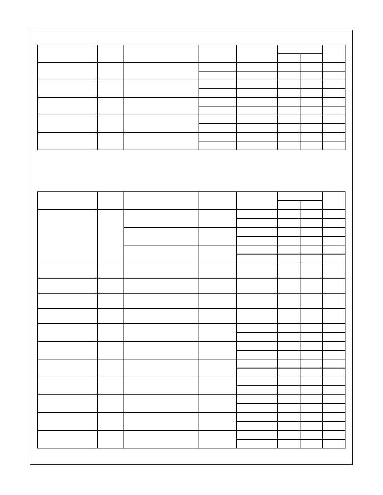
TABLE 2. AC ELECTRICAL PERFORMANCE CHARACTERISTICS
GROUP A
PARAMETER SYMBOL CONDITIONS (NOTES 1, 2)
Propagation Delay
Clock to Output
Propagation Delay
Clear to Out
Propagation Delay
Cascade to Out
Transition Time TTHL
TPHL1
TPLH1
TPHL2
TPLH2
TPHL3
TPLH3
VDD = 5V, VIN = VDD or GND 9 +25oC - 300 ns
VDD = 5V, VIN = VDD or GND 9 +25oC - 760 ns
VDD = 5V, VIN = VDD or GND 9 +25oC - 180 ns
VDD = 5V, VIN = VDD or GND 9 +25oC - 200 ns
TTLH
Maximum Clock Input
FCL VDD = 5V, VIN = VDD or GND 9 +25oC 1.2 - MHz
Frequency
NOTES:
1. CL = 50pF, RL = 200K, Input TR, TF < 20ns.
2. -55oC and +125oC limits guaranteed, 100% testing being implemented.
TABLE 3. ELECTRICAL PERFORMANCE CHARACTERISTICS
PARAMETER SYMBOL CONDITIONS NOTES TEMPERATURE
Supply Current IDD VDD = 5V, VIN = VDD or GND 1, 2 -55
VDD = 10V, VIN = VDD or GND 1, 2 -55
VDD = 15V, VIN = VDD or GND 1, 2 -55
Output Voltage VOL5 VDD = 5V, No Load 1, 2 +25
Output Voltage VOL10 VDD = 10V, No Load 1, 2 +25
Output Voltage VOH5 VDD = 5V, No Load 1, 2 +25
Output Voltage VOH10 VDD = 10V, No Load 1, 2 +25
Output Current (Sink) IOL5 VDD = 5V, VOUT = 0.4V 1, 2 +125
Output Current (Sink) IOL10 VDD = 10V, VOUT = 0.5V 1, 2 +125
Output Current (Sink) IOL15 VDD = 15V, VOUT = 1.5V 1, 2 +125
Output Current (Source) IOH5A VDD = 5V, VOUT = 4.6V 1, 2 +125
Output Current (Source) IOH5B VDD = 5V, VOUT = 2.5V 1, 2 +125
Output Current (Source) IOH10 VDD = 10V, VOUT = 9.5V 1, 2 +125
Output Current (Source) IOH15 VDD =15V, VOUT = 13.5V 1, 2 +125
SUBGROUPS TEMPERATURE
10, 11 +125oC, -55oC - 405 ns
10, 11 +125oC, -55oC - 1026 ns
10, 11 +125oC, -55oC - 243 ns
10, 11 +125oC, -55oC - 270 ns
10, 11 +125oC, -55oC .89 - MHz
o
+125
o
+125
o
+125
o
C, +125oC,
-55oC
o
C, +125oC,
-55oC
o
C, +125oC,
-55oC
o
C, +125oC,
-55oC
-55
-55
-55
-55
-55
-55
-55
LIMITS
UNITSMIN MAX
LIMITS
UNITSMIN MAX
C, +25oC- 5 µA
o
C - 150 µA
C, +25oC- 10µA
o
C - 300 µA
C, +25oC- 10µA
o
C - 600 µA
-50mV
-50mV
4.95 - V
9.95 - V
o
C 0.36 - mA
o
C 0.64 - mA
o
C 0.9 - mA
o
C 1.6 - mA
o
C 2.4 - mA
o
C 4.2 - mA
o
C - -0.36 mA
o
C - -0.64 mA
o
C - -1.15 mA
o
C - -2.0 mA
o
C - -0.9 mA
o
C - -1.6 mA
o
C - -2.4 mA
o
C - -4.2 mA
7-1066
 Loading...