Intersil Corporation CD4076BMS Datasheet

CD4076BMS
December 1992
Features
• High Voltage Type (20V Rating)
• Three State Outputs
• Input Disabled Without Gating the Clock
• Gated Output Control Lines for Enabling or Disabling
the Outputs
• Standardized Symmetrical Output Characteristics
• 100% Tested for Quiescent Current at 20V
• Maximum Input Current of 1µA at 18V Over Full Package Temperature Range; 100nA at 18V and +25
• Noise Margin (Over Full Package/Temperature Range)
- 1V at VDD = 5V
- 2V at VDD = 10V
- 2.5V at VDD = 15V
• 5V, 10V and 15V Parametric Ratings
• Meets All Requirements of JEDEC Tentative Standard
No. 13B, “Standard Specifications for Description of
‘B’ Series CMOS Devices”
Description
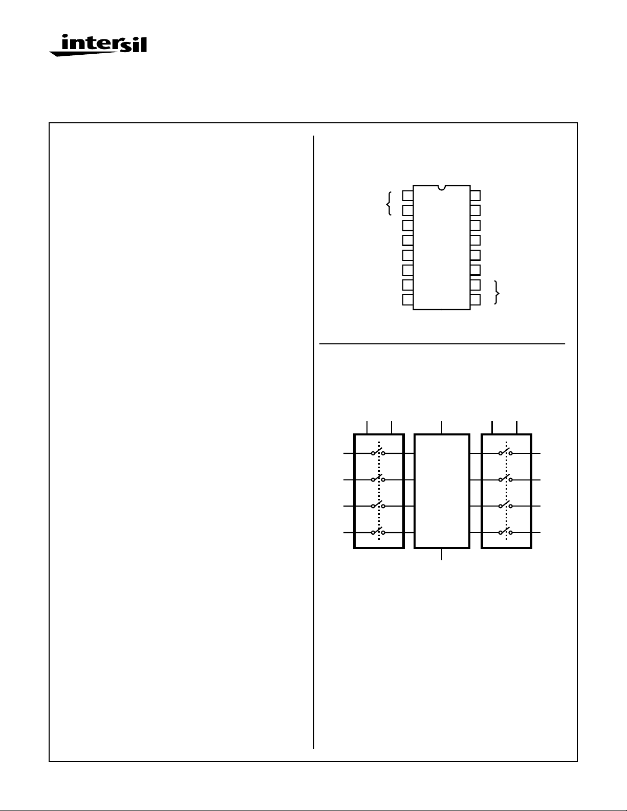
CD4076BMS types are four-bit registers consisting of D-type
flip-flops that feature three-state outputs. Data Disable inputs
are provided to control the entry of data into the flip-flops.
When both Data Disable inputs are low, data at the D inputs
are loaded into their respective flip-flops on the next positive
transition of the clock input. Output Disable inputs are also
provided. When the Output Disable inputs are both low, the
normal logic states of the four outputs are available to the
load. The outputs are disabled independently of the clock by
a high logic level at either Output Disable input, and present
a high impedance.
The CD4076BMS is supplied in these 16 lead outline packages:
CMOS 4 -Bit D-Type Registers
Pinout
CD4076BMS
TOP VIEW
16
15
14
13
12
11
10
9
VSS = 8
VDD = 16
VDD
RESET
DATA 1
DATA 2
DATA 3
DATA 4
G2
G1
OUTPUT
DISABLE
DATA
INPUT
DISABLE
3
Q1
4
Q2
5
Q3
6
Q4
1
Q1
Q2
Q3
Q4
CLOCK
VSS
M
2
N
3
4
5
6
7
8
OUTPUT
DISABLE
o
C
Functional Diagram
DATA INPUT
DISABLE
G1 G2 M N
910 1 2
14
D1
13
D2
12
D3
11
D4
CLOCK
7
4D - TYPE
FLIP-FLOPS
WITH
AND-OR
LOGIC
15
RESET
Braze Seal DIP H4T
Frit Seal DIP H1E
Ceramic Flatpack H6W
CAUTION: These devices are sensitive to electrostatic discharge; follow proper IC Handling Procedures.
1-888-INTERSIL or 321-724-7143 | Copyright © Intersil Corporation 1999
7-1029
File Number
3325

Specifications CD4076BMS
Absolute Maximum Ratings Reliability Information
DC Supply Voltage Range, (VDD) . . . . . . . . . . . . . . . -0.5V to +20V
(Voltage Referenced to VSS Terminals)
Input Voltage Range, All Inputs . . . . . . . . . . . . .-0.5V to VDD +0.5V
DC Input Current, Any One Input . . . . . . . . . . . . . . . . . . . . . . . .±10mA
Operating Temperature Range. . . . . . . . . . . . . . . . -55
Package Types D, F, K, H
Storage Temperature Range (TSTG). . . . . . . . . . . -65
o
C to +125oC
o
C to +150oC
Lead Temperature (During Soldering) . . . . . . . . . . . . . . . . . +265
At Distance 1/16 ± 1/32 Inch (1.59mm ± 0.79mm) from case for
10s Maximum
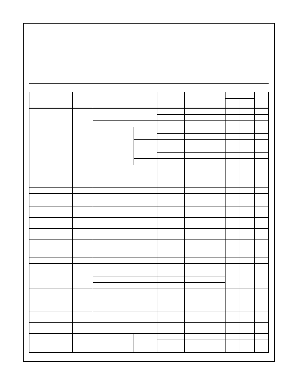
TABLE 1. DC ELECTRICAL PERFORMANCE CHARACTERISTICS
PARAMETER SYMBOL CONDITIONS (NOTE 1)
Supply Current IDD VDD = 20V, VIN = VDD or GND 1 +25oC-10µA
VDD = 18V, VIN = VDD or GND 3 -55
Input Leakage Current IIL VIN = VDD or GND VDD = 20 1 +25oC -100 - nA
VDD = 18V 3 -55oC -100 - nA
Input Leakage Current IIH VIN = VDD or GND VDD = 20 1 +25oC - 100 nA
VDD = 18V 3 -55oC - 100 nA
Output Voltage VOL15 VDD = 15V, No Load 1, 2, 3 +25oC, +125oC, -
Output Voltage VOH15 VDD = 15V, No Load (Note 3) 1, 2, 3 +25oC, +125oC, -
Output Current (Sink) IOL5 VDD = 5V, VOUT = 0.4V 1 +25oC 0.53 - mA
Output Current (Sink) IOL10 VDD = 10V, VOUT = 0.5V 1 +25oC 1.4 - mA
Output Current (Sink) IOL15 VDD = 15V, VOUT = 1.5V 1 +25oC 3.5 - mA
Output Current
IOH5A VDD = 5V, VOUT = 4.6V 1 +25oC - -0.53 mA
(Source)
Output Current
IOH5B VDD = 5V, VOUT = 2.5V 1 +25oC - -1.8 mA
(Source)
Output Current
IOH10 VDD = 10V, VOUT = 9.5V 1 +25oC - -1.4 mA
(Source)
Output Current
IOH15 VDD = 15V, VOUT = 13.5V 1 +25oC - -3.5 mA
(Source)
N Threshold Voltage VNTH VDD = 10V, ISS = -10µA 1 +25oC -2.8 -0.7 V
P Threshold Voltage VPTH VSS = 0V, IDD = 10µA 1 +25oC 0.7 2.8 V
Functional F VDD = 2.8V, VIN = VDD or GND 7 +25oC VOH >
VDD = 20V, VIN = VDD or GND 7 +25oC
VDD = 18V, VIN = VDD or GND 8A +125oC
VDD = 3V, VIN = VDD or GND 8B -55oC
Input Voltage Low
VIL VDD = 5V, VOH > 4.5V, VOL < 0.5V 1, 2, 3 +25oC, +125oC, -
(Note 2)
Input Voltage High
VIH VDD = 5V, VOH > 4.5V, VOL < 0.5V 1, 2, 3 +25oC, +125oC, -
(Note 2)
Input Voltage Low
(Note 2)
Input Voltage High
(Note 2)
Tri-State Output
Leakage
VIL VDD = 15V, VOH > 13.5V,
VOL < 1.5V
VIH VDD = 15V, VOH > 13.5V,
VOL < 1.5V
IOZL VIN = VDD or GND
VOUT = 0V
VDD = 20V 1 +25oC -0.4 - µA
VDD = 18V 3 -55oC -0.4 - µA
Thermal Resistance . . . . . . . . . . . . . . . . θ
Ceramic DIP and FRIT Package. . . . . 80oC/W 20oC/W
Flatpack Package . . . . . . . . . . . . . . . . 70
Maximum Package Power Dissipation (PD) at +125oC
For TA = -55
For TA = +100
o
C
Device Dissipation per Output Transistor . . . . . . . . . . . . . . . 100mW
o
C to +100oC (Package Type D, F, K). . . . . . 500mW
o
C to +125oC (Package Type D, F, K) . . . . .Derate
Linearity at 12mW/oC to 200mW
ja
o
C/W 20oC/W
For TA = Full Package Temperature Range (All Package Types)
Junction Temperature . . . . . . . . . . . . . . . . . . . . . . . . . . . . . . +175oC
GROUP A
LIMITS
SUBGROUP
S TEMPERATURE
o
2 +125
C - 1000 µA
o
C-10µA
2 +125oC -1000 - nA
2 +125oC - 1000 nA
-50mV
55oC
14.95 - V
55oC
VOL
VDD/2
VDD/2
- 1.5 V
55oC
3.5 - V
55oC
1, 2, 3 +25oC, +125oC, -
-4V
55oC
1, 2, 3 +25oC, +125oC, -
11 - V
55oC
2 +125oC -12 - µA
θ
jc
UNIT
<
SMIN MAX
V
7-1030

Specifications CD4076BMS
TABLE 1. DC ELECTRICAL PERFORMANCE CHARACTERISTICS
GROUP A
SUBGROUP
PARAMETER SYMBOL CONDITIONS (NOTE 1)
Tri-State Output
Leakage
NOTES: 1. All voltages referenced to device GND, 100% testing being
implemented.
2. Go/No Go test with limits applied to inputs.
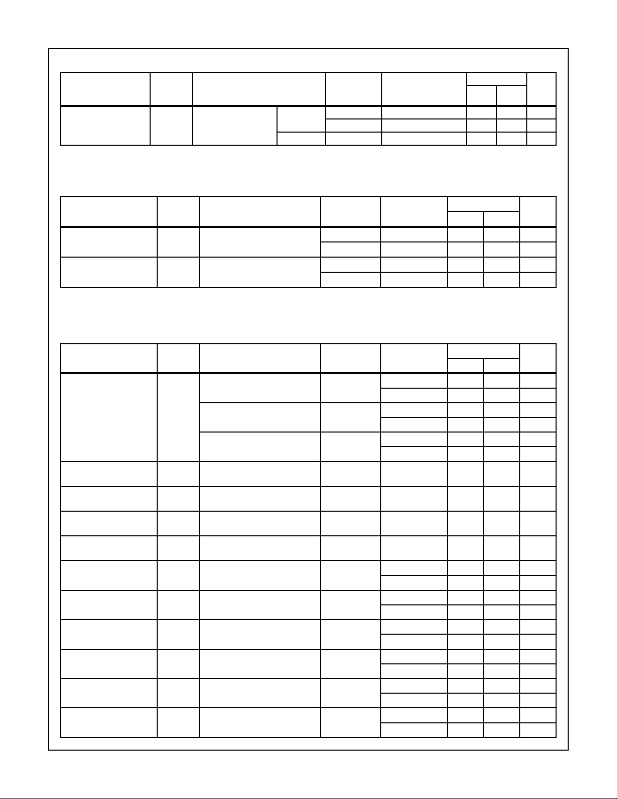
PARAMETER SYMBOL CONDITIONS (Notes 1, 2)
Propagation Delay
Clock to Q Output
Transition Time TTHL
NOTES:
1. CL = 50pF, RL = 200K, Input TR, TF < 20ns.
2. -55oC and +125oC limits guaranteed, 100% testing being implemented.
PARAMETER SYMBOL CONDITIONS NOTES TEMPERATURE
Supply Current IDD VDD = 5V, VIN = VDD or GND 1, 2 -55oC, +25oC- 5 µA
Output Voltage VOL VDD = 5V, No Load 1, 2 +25oC, +125oC,
Output Voltage VOL VDD = 10V, No Load 1, 2 +25oC, +125oC,
Output Voltage VOH VDD = 5V, No Load 1, 2 +25oC, +125oC,
Output Voltage VOH VDD = 10V, No Load 1, 2 +25oC, +125oC,
Output Current (Sink) IOL5 VDD = 5V, VOUT = 0.4V 1, 2 +125oC 0.36 - mA
Output Current (Sink) IOL10 VDD = 10V, VOUT = 0.5V 1, 2 +125oC 0.9 - mA
Output Current (Sink) IOL15 VDD = 15V, VOUT = 1.5V 1, 2 +125oC 2.4 - mA
Output Current (Source) IOH5A VDD = 5V, VOUT = 4.6V 1, 2 +125oC - -0.36 mA
Output Current (Source) IOH5B VDD = 5V, VOUT = 2.5V 1, 2 +125oC - -1.15 mA
Output Current (Source) IOH10 VDD = 10V, VOUT = 9.5V 1, 2 +125oC - -0.9 mA
IOZH VIN = VDD or GND
VOUT = VDD
TABLE 2. AC ELECTRICAL PERFORMANCE CHARACTERISTICS
TPHL
TPLH
TTLH
VDD = 5V, VIN = VDD or GND 9 +25oC - 600 ns
VDD = 5V, VIN = VDD or GND 9 +25oC - 200 ns
TABLE 3. ELECTRICAL PERFORMANCE CHARACTERISTICS
VDD = 10V, VIN = VDD or GND 1, 2 -55oC, +25oC- 10µA
VDD = 15V, VIN = VDD or GND 1, 2 -55oC, +25oC- 10µA
VDD = 20V 1 +25oC - 0.4 µA
VDD = 18V 3 -55oC - 0.4 µA
S TEMPERATURE
2 +125oC-12µA
3. For accuracy, voltage is measured differentially to VDD.
Limit is 0.050V max.
GROUP A
SUBGROUPS TEMPERATURE
10, 11 +125oC, -55oC - 810 ns
10, 11 +125oC, -55oC - 270 ns
+125oC - 150 µA
+125oC - 300 µA
+125oC - 600 µA
-55oC
-55oC
-55oC
-55oC
-55oC 0.64 - mA
-55oC 1.6 - mA
-55oC 4.2 - mA
-55oC - -0.64 mA
-55oC - -2.0 mA
-55oC - -2.6 mA
LIMITS
LIMITS
UNITSMIN MAX
LIMITS
UNITSMIN MAX
-50mV
-50mV
4.95 - V
9.95 - V
UNIT
SMIN MAX
7-1031
 Loading...