Intersil Corporation CD4051BMS, CD4053BMS, CD4052BMS Datasheet

December 1992
CD4051BMS, CD4052BMS
CD4053BMS
CMOS Analog
Multiplexers/Demultiplexers*
Features
• Logic Level Conversion
• High-Voltage Types (20V Rating)
• CD4051BMS Signal 8-Channel
• CD4052BMS Differential 4-Channel
• CD4053BMS Triple 2-Channel
• Wide Range of Digital and Analog Signal Levels:
- Digital 3V to 20V
- Analog to 20Vp-p
• Low ON Resistance: 125Ω (typ) Over 15Vp-p Signal
Input Range for VDD - VEE = 15V
• High OFF Resistance: Channel Leakage of ±100pA
(typ) at VDD - VEE = 18V
• Logic Level Conversion:
- Digital Addressing Signals of 3V to 20V (VDD - VSS
= 3V to 20V)
- Switch Analog Signals to 20Vp-p (VDD - VEE = 20V);
See Introductory Text
• Matched Switch Characteristics: RON = 5Ω (typ) for
VDD - VEE = 15V
• Very Low Quiescent Power Dissipation Under All Digi-
tal Control Input and Supply Conditions: 0.2µW (typ)
at VDD - VSS = VDD - VEE = 10V
• Binary Address Decoding on Chip
• 5V, 10V and 15V Parametric Ratings
• 100% Tested for Quiescent Current at 20V
• Maximum Input Current of 1µA at 18V Over Full Pack-
age Temperature Range; 100nA at 18V and +25
• Break-Before-Making Switching Eliminates Channel
Overlap
o
C
Applications
Description
CD4051BMS, CD4052BMS and CD4053BMS analog multiplexers/demultiplexers are digitally controlled analog
switches having low ON impedance and very low OFF leakage current. Control of analog signals up to 20V peak-topeak can be achieved by digital signal amplitudes of 4.5V to
20V (if VDD-VSS = 3V , a VDD-VEE of up to 13V can be controlled; for VDD-VEE level differences above 13V, a VDDVSS of at least 4.5V is required). For example, if VDD =
+4.5V, VSS = 0, and VEE = -13.5V, analog signals from -
13.5V to +4.5V can be controlled by digital inputs of 0 to 5V.
These multiplexer circuits dissipate extremely low quiescent
power over the full VDD-VSS and VDD-VEE supply voltage
ranges, independent of the logic state of the control signals.
When a logic “1” is present at the inhibit input terminal all
channels are off.
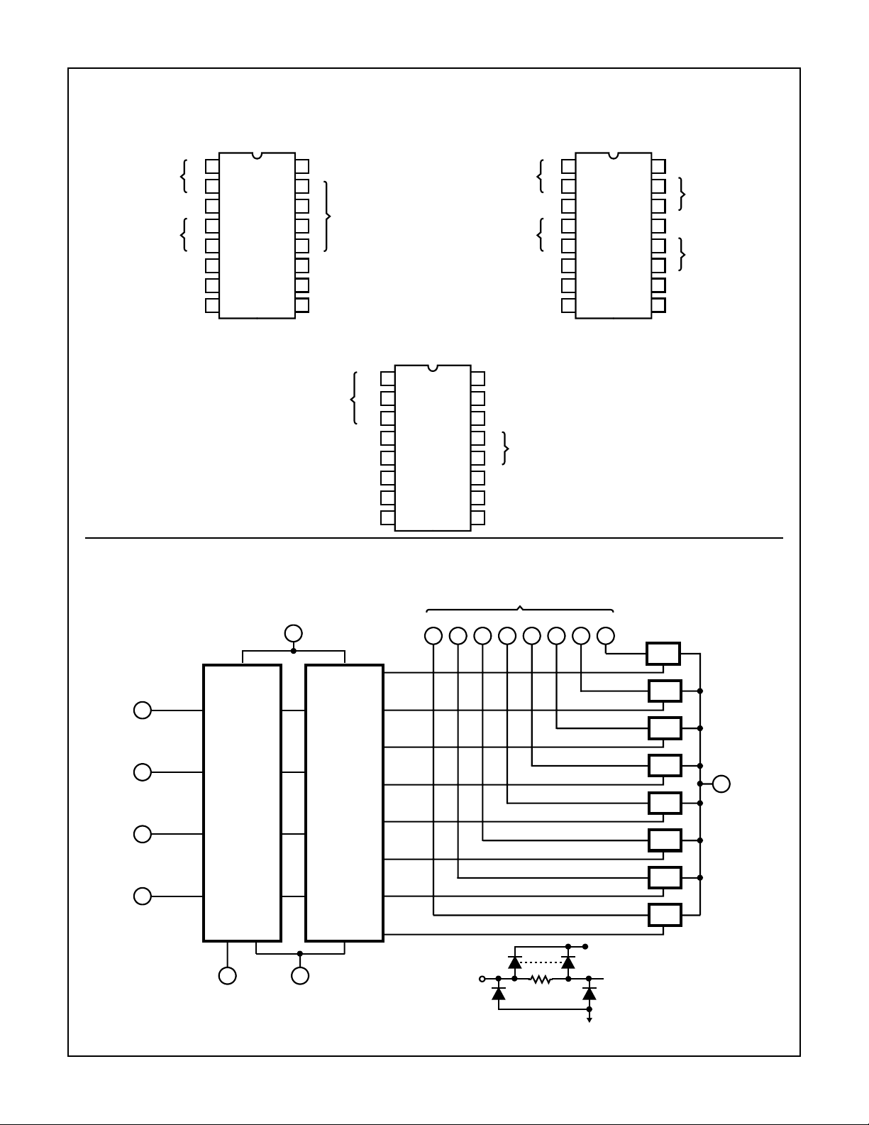
The CD4051BMS is a single 8 channel multiplexer having
three binary control inputs, A, B, and C, and an inhibit input.
The three binary signals select 1 of 8 channels to be turned
on, and connect one of the 8 inputs to the output.
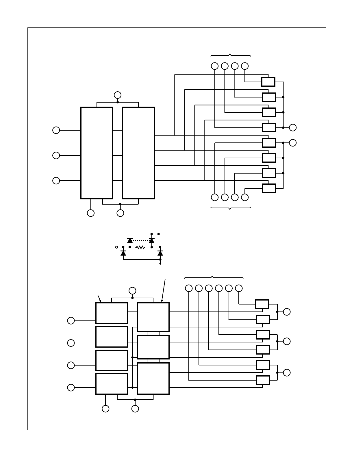
The CD4052BMS is a differential 4 channel multiplexer having two binary control inputs, A and B, and an inhibit input.
The two binary input signals select 1 of 4 pairs of channels
to be turned on and connect the analog inputs to the outputs.
The CD4053BMS is a triple 2 channel multiplexer having
three separate digital control inputs, A, B, and C, and an
inhibit input. Each control input selects one of a pair of channels which are connected in a single pole double-throw configuration.
The CD4051BMS, CD4052BMS and CD4053BMS are supplied
in these 16 lead outline packages:
Braze Seal DIP *H4X †H4T
Frit Seal DIP H1E
Ceramic Flatpack H6W
*CD4051B Only †CD4052B, CD4053 Only
• Analog and Digital Multiplexing and Demultiplexing
• A/D and D/A Conversion
• Signal Gating
* When these devices are used as demultiplexers the “CHANNEL
IN/OUT” terminals are the outputs and the “COMMON OUT/IN” terminals are the inputs.
CAUTION: These devices are sensitive to electrostatic discharge; follow proper IC Handling Procedures.
1-888-INTERSIL or 321-724-7143 | Copyright © Intersil Corporation 1999
7-937
File Number 3316

Pinouts
CD4051BM
TOP VIEW
CD4051BMS, CD4052BMS, CD4053BMS
CD4052BMS
TOP VIEW
1
INH
VEE
VSS
4
2
6
3
4
7
5
5
6
7
8
CHANNELS
IN/OUT
COM OUT/IN
CHANNELS
IN/OUT
Functional Diagrams
16
VDD
15
2
14
1
CHANNELS
IN/OUT
13
0
12
3
11
A
10
B
9
C
by
IN/OUT
OUT/IN CX or CY
bx
cy
IN/OUT CX
INH
VEE
VSS
CD4053BMS
TOP VIEW
1
2
3
4
5
6
7
8
Y CHANNELS
IN/OUT
COMMON “Y” OUT/IN
Y CHANNELS
IN/OUT
INH
VEE
VSS
16
VDD
OUT/IN bx or by
15
OUT/IN ax or ay
14
13
ay
IN/OUT
ax
12
A
11
B
10
9
C
16
1
0
2
2
3
4
3
5
1
6
7
8
VDD
15
2
X CHANNELS
IN/OUT
14
1
13
COMMON “X” OUT/IN
12
0
X CHANNELS
IN/OUT
11
3
10
A
9
B
INH
CHANNEL IN/OUT
76543210
16
VDD
*
11
A
*
10
B
LOGIC
LEVEL
CONVERSION
*
9
C
BINARY
TO
1 OF 8
DECODER
WITH
INHIBIT
*
6
8
VEEVSS
7
124 5 12 131415
TG
TG
TG
TG
TG
TG
TG
TG
VDD
* ALL INPUTS PROTECTED BY
STANDARD CMOS PROTECTION
NETWORK
3
COMMON
OUT/IN
CD4051BMS
7-938
VSS

CD4051BMS, CD4052BMS, CD4053BMS
Functional Diagrams (Continued)
16
VDD
X CHANNELS IN/OUT
3210
11 121415
TG
TG
INH
TG
*
10
A
*
9
B
LOGIC
LEVEL
CONVERSION
BINARY
TO
1 OF 4
DECODER
WITH
INHIBIT
*
6
1425
0123
8
7
VEEVSS
Y CHANNELS IN/OUT
TG
TG
TG
TG
TG
COMMON X
OUT/IN
13
3
COMMON Y
OUT/IN
CD4052BMS
VDD
* ALL INPUTS PROTECTED BY
STANDARD CMOS PROTECTION
NETWORK
VSS
IN/OUT
by bx ay ax
112132
TG
TG
TG
TG
TG
TG
OUT/IN
ax or ay
14
OUT/IN
bx or by
15
OUT/IN
cx or cy
4
INH
A
B
C
LOGIC
LEVEL
CONVERSION
*
11
*
10
*
9
*
6
BINARY TO 1 OF 2
DECODERS WITH
INHIBIT
16
VDD
cy cx
35
8
7
VEEVSS
CD4053BMS
7-939

Specifications CD4051BMS, CD4052BMS, CD4053BMS
Absolute Maximum Ratings Reliability Information
DC Supply Voltage Range, (VDD) . . . . . . . . . . . . . . . -0.5V to +20V
(Voltage Referenced to VSS Terminals)
Input Voltage Range, All Inputs . . . . . . . . . . . . .-0.5V to VDD +0.5V
DC Input Current, Any One Input . . . . . . . . . . . . . . . . . . . . . . . .±10mA
Operating Temperature Range. . . . . . . . . . . . . . . . -55
Package Types D, F, K, H
Storage Temperature Range (TSTG). . . . . . . . . . . -65
o
C to +125oC
o
C to +150oC
Lead Temperature (During Soldering) . . . . . . . . . . . . . . . . . +265
At Distance 1/16 ± 1/32 Inch (1.59mm ± 0.79mm) from case for
10s Maximum
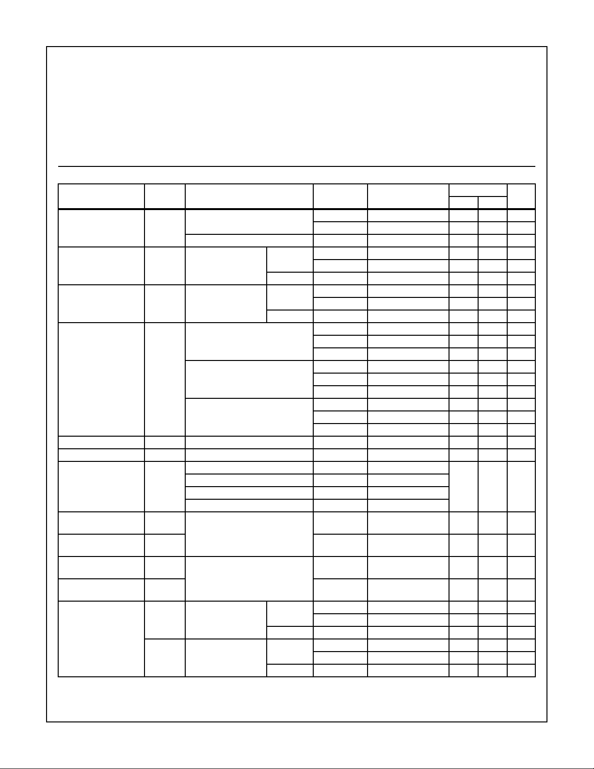
TABLE 1. DC ELECTRICAL PERFORMANCE CHARACTERISTICS
PARAMETER SYMBOL CONDITIONS (NOTE 1)
Supply Current IDD VDD = 20V, VIN = VDD or GND 1 +25oC-10µA
VDD = 18V, VIN = VDD or GND 3 -55
Input Leakage Current IIL VIN = VDD or GND VDD = 20 1 +25
VDD = 18V 3 -55oC -100 - nA
Input Leakage Current IIH VIN = VDD or GND VDD = 20 1 +25oC - 100 nA
VDD = 18V 3 -55oC - 100 nA
On-State Resistance
RL = 10K Returned to
RON VDD = 5V
VIS = VSS to VDD
VDD - VSS/2
VDD = 10V
VIS = VSS to VDD
VDD = 15V
VIS = VSS to VDD
N Threshold Voltage VNTH VDD = 10V, ISS = -10µA 1 +25oC -2.8 -0.7 V
P Threshold Voltage VPTH VSS = 0V, IDD = 10µA 1 +25oC 0.7 2.8 V
Functional
(Note 4)
F VDD = 2.8V, VIN = VDD or GND 7 +25oC VOH >
VDD = 20V, VIN = VDD or GND 7 +25oC
VDD = 18V, VIN = VDD or GND 8A +125oC
VDD = 3V, VIN = VDD or GND 8B -55oC
Input Voltage Low
(Note 2)
Input Voltage High
(Note 2)
Input Voltage Low
(Note 2)
Input Voltage High
(Note 2)
Off Channel Leakage
Any Channel OFF
Or
All Channels Off
(Common Out/In)
VIL VDD = 5V = VIS thru 1k,
VEE = VSS
VIH 1, 2, 3 +25oC, +125oC, -55oC 3.5 - V
RL = 1k to VSS, |IIS| < 2µA
OFF Channels
VIL VDD = 15V = VIS thru 1K
VEE = VSS
VIH 1, 2, 3 +25oC, +125oC, -55oC11 - V
IOZL VIN = VDD or GND
RL = 1K to VSS, |ISS|, <2µA
On All OFF Channels
VDD = 20V 1 +25oC -0.1 - µA
VOUT = 0V
VDD = 18V 3 -55oC -0.1 - µA
IOZH VIN = VDD or GND
VDD = 20V 1 +25oC - 0.1 µA
VOUT = VDD
VDD = 18V 3 -55oC - 0.1 µA
NOTES: 1. All voltages referenced to device GND, 100% testing being
implemented.
2. Go/No Go test with limits applied to inputs.
Thermal Resistance . . . . . . . . . . . . . . . . θ
Ceramic DIP and FRIT Package. . . . . 80oC/W 20oC/W
Flatpack Package . . . . . . . . . . . . . . . . 70
Maximum Package Power Dissipation (PD) at +125oC
For TA = -55
For TA = +100
o
C
Device Dissipation per Output Transistor . . . . . . . . . . . . . . . 100mW
o
C to +100oC (Package Type D, F, K). . . . . . 500mW
o
C to +125oC (Package Type D, F, K) . . . . .Derate
Linearity at 12mW/oC to 200mW
ja
o
C/W 20oC/W
For TA = Full Package Temperature Range (All Package Types)
Junction Temperature . . . . . . . . . . . . . . . . . . . . . . . . . . . . . . +175oC
GROUP A
LIMITS
SUBGROUPS TEMPERATURE
2 +125oC - 1000 µA
o
C-10µA
o
C -100 - nA
2 +125oC -1000 - nA
2 +125oC - 1000 nA
1 +25oC - 1050 Ω
2 +125oC - 1300 Ω
3 -55oC - 800 Ω
1 +25oC - 400 Ω
2 +125oC - 550 Ω
3 -55oC - 310 Ω
1 +25oC - 240 Ω
2 +125oC - 320 Ω
3 -55oC - 220 Ω
VOL <
VDD/2
VDD/2
1, 2, 3 +25oC, +125oC, -55oC - 1.5 V
1, 2, 3 +25oC, +125oC, -55oC- 4 V
2 +125oC -1.0 - µA
2 +125oC - 1.0 µA
3. For accuracy, voltage is measured differentially to VDD. Limit
is 0.050V max.
4. VDD = 2.8V/3.0V, RL = 200k to VDD
VDD = 20V/18V, RL = 10k to VDD
θ
jc
UNITSMIN MAX
V
7-940
 Loading...