Intersil Corporation CD4049UBMS Datasheet

CD4049UBMS
Data Sheet December 1992 File Number 3315
CMOS Hex Buffer/Converter
The CD4049UBMS is an inverting hex buffer and features
logic level conversion using only one supply (voltage (VCC).
The input signalhigh level (VIH) can exceed the VCC supply
voltage when this device is used for logic level conversions.
This device is intended for use as CMOS to DTL/TTL
converters and can drive directly two DTL/TTL loads. (VCC
= 5V, VOL ≤ 0.4V, and IOL ≥ 3.3mA.
The CD4049UBMS is designated as replacement for
CD4009UB. Because the CD4049UBMS requires only one
power supply, it is preferred over the CD4009UB and
CD4010B and should be used in place of the CD4009UB in
all inverter, current driver, or logic level conversion applications. In these applications the CD4049UBMS is pin compatible with the CD4009UB, and can be substituted for this
device in existing as well as in new designs. Terminal No. 16
is not connected internally on the CD4049UBMS, therefore,
connection to this terminal is of no consequence to circuit
operation. For applications not requiring high sink current or
voltage conversion, the CD4069UB Hex Inverter is recommended.
The CD4049UBMS is supplied in these 16 lead outline packages:
Braze Seal DIP H4S
Frit Seal DIP H1E
Ceramic Flatpack H3X
Features
• High Voltage Type (20V Rating)
• Inverting Type
• High Sink Current for Driving 2 TTL Loads
• High-to-Low Level Logic Conversion
• 100% Tested for Quiescent Current at 20V
• Maximum Input Current of 1µA at 18V Over Full Pack-
age Temperature Range; 100nA at 18V and +25
o
C
• 5V, 10V and 15V Parametric Ratings
Applications
• CMOS to DTL/TTL Hex Converter
• CMOS Current “Sink” or “Source” Driver
• CMOS High-to-Low Logic Level Converter
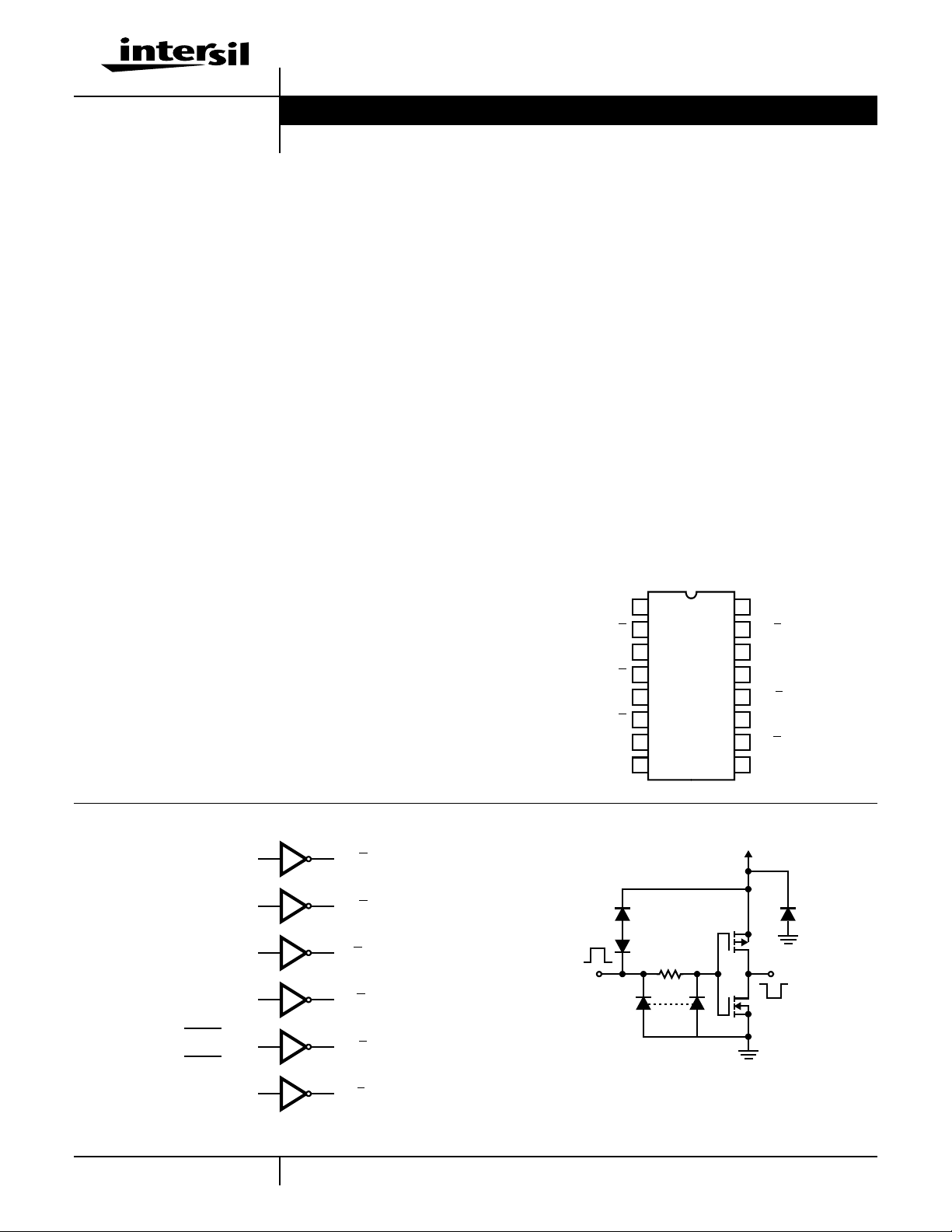
Pinout
G = A
H =
VCC
I =
VSS
A
B
B
C
C
CD4049UBMS
TOP VIEW
1
2
3
4
5
6
7
8
16
NC
15
F
L =
14
F
13
NC
12
E
K =
E
11
J =
10
D
9
D
Functional Diagram Schematic
VCC
VSS
NC = 13
NC = 16
32
AG =
54
BH =
76
CI =
910
DJ =
1
8
11 12
EK =
14 15
FL =
1
A
B
C
IN
D
E
F
CAUTION: These devices are sensitive to electrostatic discharge; follow proper IC Handling Procedures.
FIGURE 1. SCHEMATIC DIAGRAM, 1 OF 6 IDENTICAL UNITS
1-888-INTERSIL or 321-724-7143 | Copyright © Intersil Corporation 1999
VCC
P
R
OUT
N
VSS

CD4049UBMS
Absolute Maximum Ratings Reliability Information
DC Supply Voltage Range, (VDD) . . . . . . . . . . . . . . . .-0.5V to +20V
(Voltage Referenced to VSS Terminals)
Input Voltage Range, All Inputs . . . . . . . . . . . . . -0.5V to VDD +0.5V
DC Input Current, Any One Input. . . . . . . . . . . . . . . . . . . . . . . . .±10mA
Operating Temperature Range . . . . . . . . . . . . . . . -55oC to +125oC
Package Types D, F, K, H
Storage Temperature Range (TSTG). . . . . . . . . . . -65oC to +150oC
Lead Temperature (During Soldering) . . . . . . . . . . . . . . . . . +265oC
At Distance 1/16 ± 1/32 Inch (1.59mm ± 0.79mm) from case for
10s Maximum
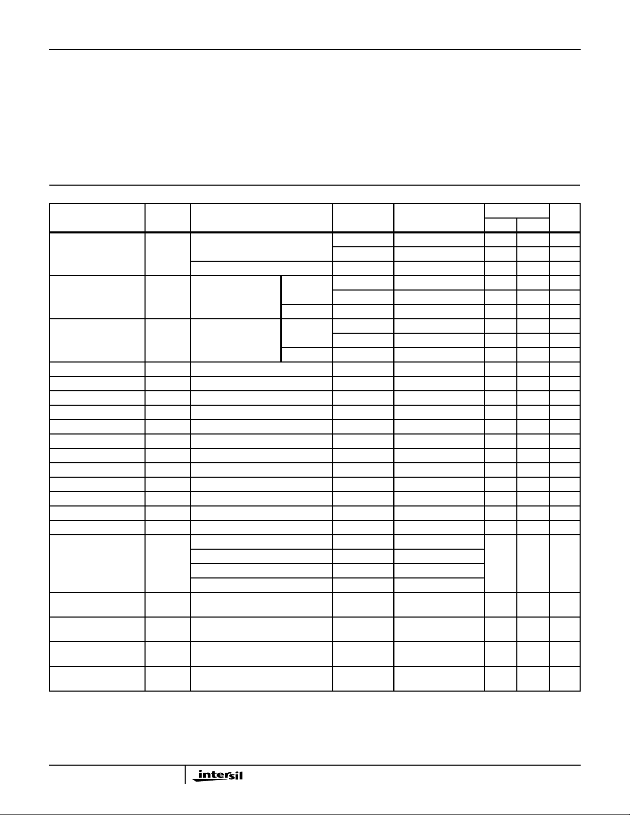
TABLE 1. DC ELECTRICAL PERFORMANCE CHARACTERISTICS
PARAMETER SYMBOL CONDITIONS (NOTE 1)
Supply Current IDD VDD = 20V, VIN = VDD or GND 1 +25oC-2µA
VDD = 18V, VIN = VDD or GND 3 -55oC-2µA
Input Leakage Current IIL VIN = VDD or GND VDD = 20 1 +25oC -100 - nA
VDD = 18V 3 -55oC -100 - nA
Input Leakage Current IIH VIN = VDD or GND VDD = 20 1 +25oC - 100 nA
VDD = 18V 3 -55oC - 100 nA
Output Voltage VOL15 VDD = 15V, No Load 1, 2, 3 +25oC, +125oC, -55oC - 50 mV
Output Voltage VOH15 VDD = 15V, No Load (Note 3) 1, 2, 3 +25oC, +125oC, -55oC 14.95 - V
Output Current (Sink) IOL4 VDD = 4.5V, VOUT = 0.4V 1 +25oC 2.6 - mA
Output Current (Sink) IOL5 VDD = 5V, VOUT = 0.4V 1 +25oC 3.2 - mA
Output Current (Sink) IOL10 VDD = 10V, VOUT = 0.5V 1 +25oC 8.0 - mA
Output Current (Sink) IOL15 VDD = 15V, VOUT = 1.5V 1 +25oC24-mA
Output Current (Source) IOH5A VDD = 5V, VOUT = 4.6V 1 +25oC - -0.8 mA
Output Current (Source) IOH5B VDD = 5V, VOUT = 2.5V 1 +25oC - -3.2 mA
Output Current (Source) IOH10 VDD = 10V, VOUT = 9.5V 1 +25oC - -1.8 mA
Output Current (Source) IOH15 VDD = 15V, VOUT = 13.5V 1 +25oC - -6.0 mA
N Threshold Voltage VNTH VDD = 10V, ISS = -10µA 1 +25oC -2.8 -0.7 V
P Threshold Voltage VPTH VSS = 0V, IDD = 10µA 1 +25oC 0.7 2.8 V
Functional F VDD = 2.8V, VIN = VDD or GND 7 +25oC VOH >
VDD = 20V, VIN = VDD or GND 7 +25oC
VDD = 18V, VIN = VDD or GND 8A +125oC
VDD = 3V, VIN = VDD or GND 8B -55oC
Input Voltage Low
(Note 2)
Input Voltage High
(Note 2)
Input Voltage Low
(Note 2)
Input Voltage High
(Note 2)
NOTES: 1. All voltages referenced to device GND, 100% testing being im-
plemented.
2. Go/No Go test with limits applied to inputs.
VIL VDD = 5V, VOH > 4.5V, VOL < 0.5V 1, 2, 3 +25oC, +125oC, -55oC - 1.0 V
VIH VDD = 5V, VOH > 4.5V, VOL < 0.5V 1, 2, 3 +25oC, +125oC, -55oC 4.0 - V
VIL VDD = 15V, VOH > 13.5V,
VOL < 1.5V
VIH VDD = 15V, VOH > 13.5V,
VOL < 1.5V
Thermal Resistance. . . . . . . . . . . . . . . . θ
Ceramic DIP and FRIT Package . . . . 80oC/W 20oC/W
Flatpack Package. . . . . . . . . . . . . . . . 70oC/W 20oC/W
Maximum Package Power Dissipation (PD) at +125oC
For TA = -55oC to +100oC (Package Type D, F, K) . . . . . .500mW
For TA = +100oC to +125oC (Package Type D, F, K) . . . . . Derate
Linearity at 12mW/oC to 200mW
Device Dissipation per Output Transistor. . . . . . . . . . . . . . . .100mW
For TA = Full Package Temperature Range (All Package Types)
Junction Temperature . . . . . . . . . . . . . . . . . . . . . . . . . . . . . .+175oC
GROUP A
SUBGROUPS TEMPERATURE
2 +125oC - 200 µA
2 +125oC -1000 - nA
2 +125oC - 1000 nA
1, 2, 3 +25oC, +125oC, -55oC - 2.5 V
1, 2, 3 +25oC, +125oC, -55oC 12.5 - V
3. Foraccuracy,voltage ismeasureddifferentially toVDD.Limit is
0.050V max.
ja
LIMITS
VDD/2
VOL <
VDD/2
θ
jc
UNITSMIN MAX
V
2

CD4049UBMS
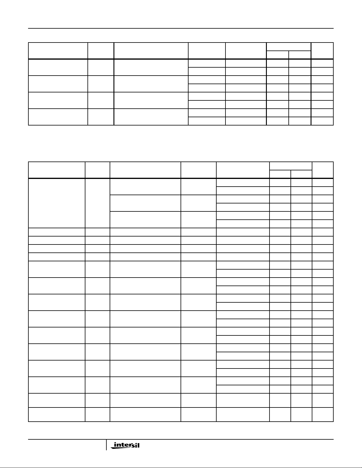
TABLE 2. AC ELECTRICAL PERFORMANCE CHARACTERISTICS
GROUP A
PARAMETER SYMBOL CONDITIONS (NOTE 1, 2)
Propagation Delay TPHL VDD = 5V, VIN = VDD or GND 9 +25oC - 65 ns
Propagation Delay TPLH VDD = 5V, VIN = VDD or GND 9 +25oC - 120 ns
Transition Time TTHL VDD = 5V, VIN = VDD or GND 9 +25oC - 60 ns
Transition Time TTLH VDD = 5V, VIN = VDD or GND 9 +25oC - 160 ns
NOTES:
1. CL = 50pF, RL = 200K, Input TR, TF < 20ns.
2. -55oC and +125oC limits guaranteed, 100% testing being implemented.
TABLE 3. ELECTRICAL PERFORMANCE CHARACTERISTICS
PARAMETER SYMBOL CONDITIONS NOTES TEMPERATURE
Supply Current IDD VDD = 5V, VIN = VDD or GND 1, 2 -55oC, +25oC-1µA
VDD = 10V, VIN = VDD or GND 1, 2 -55oC, +25oC-2µA
VDD = 15V, VIN = VDD or GND 1, 2 -55oC, +25oC-2µA
Output Voltage VOL VDD = 5V, No Load 1, 2 +25oC, +125oC, -55oC - 50 mV
Output Voltage VOL VDD = 10V, No Load 1, 2 +25oC, +125oC, -55oC - 50 mV
Output Voltage VOH VDD = 5V, No Load 1, 2 +25oC, +125oC, -55oC 4.95 - V
Output Voltage VOH VDD = 10V, No Load 1, 2 +25oC, +125oC, -55oC 9.95 - V
Output Current (Sink) IOL4 VDD = 4.5V, VOUT = 0.4V 1, 2 +125oC 1.8 - mA
Output Current (Sink) IOL5 VDD = 5V, VOUT = 0.4V 1, 2 +125oC 2.4 - mA
Output Current (Sink) IOL10 VDD = 10V, VOUT = 0.5V 1, 2 +125oC 5.6 - mA
Output Current (Sink) IOL15 VDD = 15V, VOUT = 1.5V 1, 2 +125oC18-mA
Output Current (Source) IOH5A VDD = 5V, VOUT = 4.6V 1, 2 +125oC - -0.48 mA
Output Current (Source) IOH5B VDD = 5V, VOUT = 2.5V 1, 2 +125oC - -1.55 mA
Output Current (Source) IOH10 VDD = 10V, VOUT = 9.5V 1, 2 +125oC - -1.18 mA
Output Current (Source) IOH15 VDD =15V, VOUT = 13.5V 1, 2 +125oC - -3.1 mA
Input Voltage Low VIL VDD = 10V, VOH > 9V, VOL <
1V
Input Voltage High VIH VDD = 10V, VOH > 9V, VOL <
1V
SUBGROUPS TEMPERATURE
10, 11 +125oC, -55oC - 88 ns
10, 11 +125oC, -55oC - 162 ns
10, 11 +125oC, -55oC - 81 ns
10, 11 +125oC, -55oC - 216 ns
+125oC-30µA
+125oC-60µA
+125oC - 120 µA
-55oC 3.3 - mA
-55oC 4.0 - mA
-55oC10-mA
-55oC26-mA
-55oC - -0.81 mA
-55oC - -2.6 mA
-55oC - -2.0 mA
-55oC - -5.2 mA
1, 2 +25oC, +125oC, -55oC- 2 V
1, 2 +25oC, +125oC, -55oC8 - V
LIMITS
UNITSMIN MAX
LIMITS
UNITSMIN MAX
3
 Loading...