December 1992
CD4048BMS
CMOS Multifunction
Expandable 8 Input Gate
Features
• High-Voltage Type (20V Rating)
• Three State Output
• Many Logic Functions Available in One Package
• Standardize, Symmetrical Output Characteristics
• 100% Tested for Quiescent Current at 20V
• Maximum Input Current of 1µA at 18V Over Full Pack-
age Temperature Range; 100nA at 18V and +25
o
C
• Noise Margin (Over Full Package Temperature Range):
- 1V at VDD = 5V
- 2V at VDD = 10V
- 2.5V at VDD = 15V
• 5V, 10V and 15V Parametric Ratings
• Meets All Requirements of JEDEC Tentative Standard
No. 13B, “Standard Specifications for Description of
‘B’ Series CMOS Devices”
Applications
• Selection of Up to 8 Logic Functions
• Digital Control of Logic
• General Purpose Gating Logic
- Decoding
- Encoding
Description
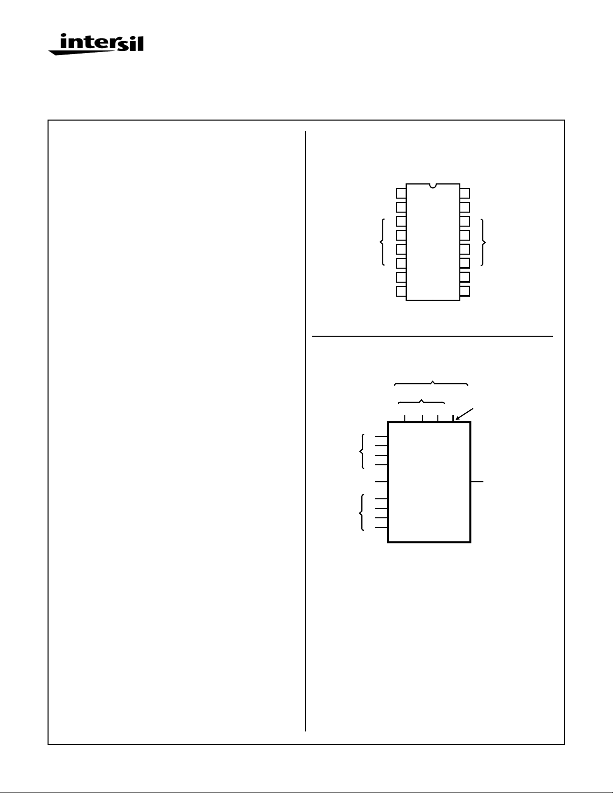
CD4048BMS is an 8-input gate having four control inputs. Three
binary control inputs - Ka, Kb, and Kc - provide the implementation of eight different logic functions. These functions are OR,
NOR, AND, NAND, OR/AND, OR/NAND, AND/OR and AND/
NOR.
A fourth control input, Kd, provides the user with a 3-state output.
When control input Kd is high, the output is either a logic 1 or a
logic 0 depending on the inner states. When control input Kd is
low, the output is an open circuit. This feature enables the user to
connect this device to a common bus line.
Pinout
CD4048BMS
TOP VIEW
Kd
Kb
VSS
1
2
3
H
4
G
5
F
6
E
7
8
J (OUTPUT)
Functional Diagram
BINARY CONTROL INPUTS
FUNCTION CONTROL
Ka Kb Kc Kd
10792
14
A
13
EXPAND
B
12
C
11
D
15
6
E
5
F
4
G
3
H
INPUTS
INPUTS
16
VDD
15
EXPAND
14
A
13
B
INPUTSINPUTS
12
C
11
D
10
Ka
9
Kc
3 STATE
CONTROL
I J OUTPUT
VSS = 8
VDD = 16
In addition to the eight input lines, an EXPAND input is provided
that permits the user to increase the number of inputs into a
CD4048BMS (see Figure 2). For example, two CD4048BMS’s
can be cascaded to provided a 16-input multifunction gate. When
the EXP AND input is not used, it should be connected to VSS.
The CD4048BMS is supplied in these 16 lead outline packages:
Braze Seal DIP H4S
Frit Seal DIP H1E
Ceramic Flatpack H6W
CAUTION: These devices are sensitive to electrostatic discharge; follow proper IC Handling Procedures.
1-888-INTERSIL or 321-724-7143 | Copyright © Intersil Corporation 1999
7-912
File Number
3314

Specifications CD4048BMS
Absolute Maximum Ratings Reliability Information
DC Supply Voltage Range, (VDD) . . . . . . . . . . . . . . . -0.5V to +20V
(Voltage Referenced to VSS Terminals)
Input Voltage Range, All Inputs . . . . . . . . . . . . .-0.5V to VDD +0.5V
DC Input Current, Any One Input . . . . . . . . . . . . . . . . . . . . . . . .±10mA
Operating Temperature Range. . . . . . . . . . . . . . . . -55
Package Types D, F, K, H
Storage Temperature Range (TSTG). . . . . . . . . . . -65
o
C to +125oC
o
C to +150oC
Lead Temperature (During Soldering) . . . . . . . . . . . . . . . . . +265
At Distance 1/16 ± 1/32 Inch (1.59mm ± 0.79mm) from case for
10s Maximum
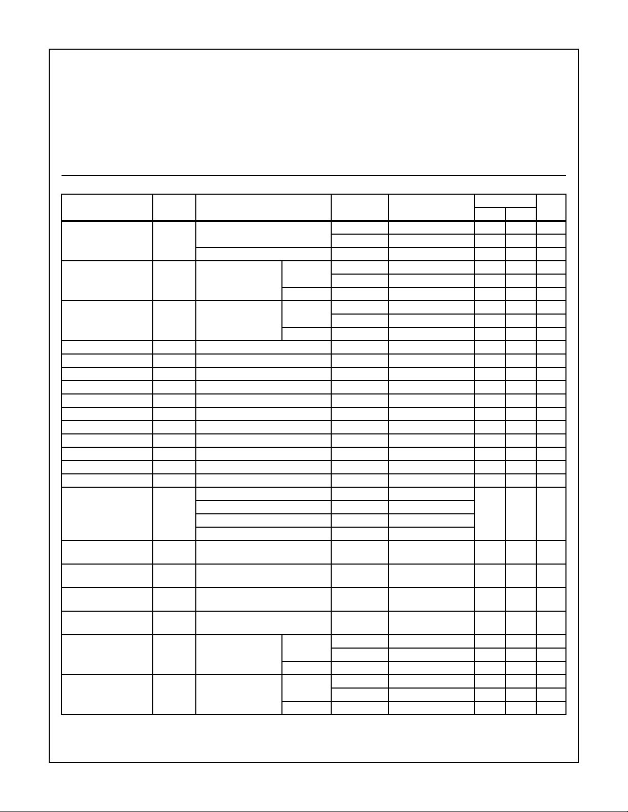
TABLE 1. DC ELECTRICAL PERFORMANCE CHARACTERISTICS
PARAMETER SYMBOL CONDITIONS (NOTE 1)
Supply Current IDD VDD = 20V, VIN = VDD or GND 1 +25oC - 0.5 µA
VDD = 18V, VIN = VDD or GND 3 -55
Input Leakage Current IIL VIN = VDD or GND VDD = 20 1 +25
VDD = 18V 3 -55oC -100 - nA
Input Leakage Current IIH VIN = VDD or GND VDD = 20 1 +25oC - 100 nA
VDD = 18V 3 -55oC - 100 nA
Output Voltage VOL15 VDD = 15V, No Load 1, 2, 3 +25oC, +125oC, -55oC - 50 mV
Output Voltage VOH15 VDD = 15V, No Load (Note 3) 1, 2, 3 +25oC, +125oC, -55oC 14.95 - V
Output Current (Sink) IOL5 VDD = 5V, VOUT = 0.4V 1 +25oC 0.53 - mA
Output Current (Sink) IOL10 VDD = 10V, VOUT = 0.5V 1 +25oC 1.4 - mA
Output Current (Sink) IOL15 VDD = 15V, VOUT = 1.5V 1 +25oC 3.5 - mA
Output Current (Source) IOH5A VDD = 5V, VOUT = 4.6V 1 +25oC - -0.53 mA
Output Current (Source) IOH5B VDD = 5V, VOUT = 2.5V 1 +25oC - -1.8 mA
Output Current (Source) IOH10 VDD = 10V, VOUT = 9.5V 1 +25oC - -1.4 mA
Output Current (Source) IOH15 VDD = 15V, VOUT = 13.5V 1 +25oC - -3.5 mA
N Threshold Voltage VNTH VDD = 10V, ISS = -10µA 1 +25oC -2.8 -0.7 V
P Threshold Voltage VPTH VSS = 0V, IDD = 10µA 1 +25oC 0.7 2.8 V
Functional F VDD = 2.8V, VIN = VDD or GND 7 +25oC VOH >
VDD = 20V, VIN = VDD or GND 7 +25oC
VDD = 18V, VIN = VDD or GND 8A +125oC
VDD = 3V, VIN = VDD or GND 8B -55oC
Input Voltage Low
VIL VDD = 5V, VOH > 4.5V, VOL < 0.5V 1, 2, 3 +25oC, +125oC, -55oC - 1.5 V
(Note 2)
Input Voltage High
VIH VDD = 5V, VOH > 4.5V, VOL < 0.5V 1, 2, 3 +25oC, +125oC, -55oC 3.5 - V
(Note 2)
Input Voltage Low
(Note 2)
Input Voltage High
(Note 2)
Tri-State Output
Leakage
VIL VDD = 15V, VOH > 13.5V,
VOL < 1.5V
VIH VDD = 15V, VOH > 13.5V,
VOL < 1.5V
IOZL VIN = VDD or GND
VOUT = 0V
VDD = 20V 1 +25oC -0.4 - µA
VDD = 18V 3 -55oC -0.4 - µA
Tri-State Output
Leakage
IOZH VIN = VDD or GND
VOUT = VDD
VDD = 20V 1 +25oC - 0.4 µA
VDD = 18V 3 -55oC - 0.4 µA
NOTES: 1. All voltages referenced to device GND, 100% testing being
implemented.
2. Go/No Go test with limits applied to inputs.
Thermal Resistance . . . . . . . . . . . . . . . . θ
Ceramic DIP and FRIT Package. . . . . 80oC/W 20oC/W
Flatpack Package . . . . . . . . . . . . . . . . 70
Maximum Package Power Dissipation (PD) at +125oC
For TA = -55
For TA = +100
o
C
Device Dissipation per Output Transistor . . . . . . . . . . . . . . . 100mW
o
C to +100oC (Package Type D, F, K). . . . . . 500mW
o
C to +125oC (Package Type D, F, K) . . . . .Derate
Linearity at 12mW/oC to 200mW
ja
o
C/W 20oC/W
For TA = Full Package Temperature Range (All Package Types)
Junction Temperature . . . . . . . . . . . . . . . . . . . . . . . . . . . . . . +175oC
GROUP A
LIMITS
SUBGROUPS TEMPERATURE
2 +125oC-50µA
o
C - 0.5 µA
o
C -100 - nA
2 +125oC -1000 - nA
2 +125oC - 1000 nA
VOL <
VDD/2
VDD/2
1, 2, 3 +25oC, +125oC, -55oC- 4 V
1, 2, 3 +25oC, +125oC, -55oC11 - V
2 +125oC -12 - µA
2 +125oC-12µA
3. For accuracy, voltage is measured differentially to VDD. Limit
is 0.050V max.
θ
jc
UNITSMIN MAX
V
7-913

Specifications CD4048BMS
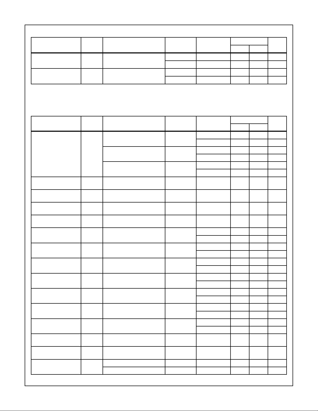
TABLE 2. AC ELECTRICAL PERFORMANCE CHARACTERISTICS
GROUP A
PARAMETER SYMBOL CONDITIONS (NOTE 1, 2)
Propagation Delay
Ka to Output
Transition Time TTHL
NOTES:
1. CL = 50pF, RL = 200K, Input TR, TF < 20ns.
2. -55oC and +125oC limits guaranteed, 100% testing being implemented.
PARAMETER SYMBOL CONDITIONS NOTES TEMPERATURE
Supply Current IDD VDD = 5V, VIN = VDD or GND 1, 2 -55oC, +25oC - 0.25 µA
Output Voltage VOL VDD = 5V, No Load 1, 2 +25oC, +125oC,
Output Voltage VOL VDD = 10V, No Load 1, 2 +25oC, +125oC,
Output Voltage VOH VDD = 5V, No Load 1, 2 +25oC, +125oC,
Output Voltage VOH VDD = 10V, No Load 1, 2 +25oC, +125oC,
Output Current (Sink) IOL5 VDD = 5V, VOUT = 0.4V 1, 2 +125oC 0.36 - mA
Output Current (Sink) IOL10 VDD = 10V, VOUT = 0.5V 1, 2 +125oC 0.9 - mA
Output Current (Sink) IOL15 VDD = 15V, VOUT = 1.5V 1, 2 +125oC 2.4 - mA
Output Current (Source) IOH5A VDD = 5V, VOUT = 4.6V 1, 2 +125oC - -0.36 mA
Output Current (Source) IOH5B VDD = 5V, VOUT = 2.5V 1, 2 +125oC - -1.15 mA
Output Current (Source) IOH10 VDD = 10V, VOUT = 9.5V 1, 2 +125oC - -0.9 mA
Output Current (Source) IOH15 VDD =15V, VOUT = 13.5V 1, 2 +125oC - -2.4 mA
Input Voltage Low VIL VDD = 10V, VOH > 9V, VOL <
Input Voltage High VIH VDD = 10V, VOH > 9V, VOL <
Propagation Delay
Ka to Output
TPHL
TPLH
TTLH
TPHL1
TPLH1
VDD = 5V, VIN = VDD or GND 9 +25oC - 600 ns
VDD = 5V, VIN = VDD or GND 9 +25oC - 200 ns
TABLE 3. ELECTRICAL PERFORMANCE CHARACTERISTICS
VDD = 10V, VIN = VDD or GND 1, 2 -55oC, +25oC - 0.5 µA
VDD = 15V, VIN = VDD or GND 1, 2 -55oC, +25oC - 0.5 µA
1V
1V
VDD = 10V 1, 2, 3 +25oC - 300 ns
VDD = 15V 1, 2, 3 +25oC - 240 ns
SUBGROUPS TEMPERATURE
10, 11 +125oC, -55oC - 810 ns
10, 11 +125oC, -55oC - 270 ns
+125oC - 7.5 µA
+125oC-15µA
+125oC-30µA
-55oC
-55oC
-55oC
-55oC
-55oC 0.64 - mA
-55oC 1.6 - mA
-55oC 4.2 - mA
-55oC - -0.64 mA
-55oC - -2.0 mA
-55oC - -1.6 mA
-55oC - -4.2 mA
1, 2 +25oC, +125oC,
-55oC
1, 2 +25oC, +125oC,
-55oC
LIMITS
UNITSMIN MAX
LIMITS
UNITSMIN MAX
-50mV
-50mV
4.95 - V
9.95 - V
-3V
7-V
7-914

Specifications CD4048BMS
TABLE 3. ELECTRICAL PERFORMANCE CHARACTERISTICS (Continued)
LIMITS
PARAMETER SYMBOL CONDITIONS NOTES TEMPERATURE
Propagation Delay
Inputs to Output
TPHL2
TPLH2
VDD = 5V 1, 2, 3 +25oC - 600 ns
VDD = 10V 1, 2, 3 +25oC - 300 ns
VDD = 15V 1, 2, 3 +25oC - 240 ns
o
Propagation Delay
Kb to Output
TPHL3
TPLH3
VDD = 5V 1, 2, 3 +25
VDD = 10V 1, 2, 3 +25
C - 450 ns
o
C - 170 ns
VDD = 15V 1, 2, 3 +25oC - 110 ns
o
Propagation Delay
Kc to Output
TPHL4
TPLH4
VDD = 5V 1, 2, 3 +25
VDD = 10V 1, 2, 3 +25
C - 280 ns
o
C - 100 ns
VDD = 15V 1, 2, 3 +25oC - 80 ns
Propagation Delay
Expand Input to Output
TPHL5
TPLH5
VDD = 5V 1, 2, 3 +25oC - 380 ns
VDD = 10V 1, 2, 3 +25oC - 180 ns
VDD = 15V 1, 2, 3 +25oC - 130 ns
Propagation Delay
3 State
Kd to Output
TPHZ, LZ
TPZH, ZL
VDD = 5V 1, 2, 4 +25oC - 160 ns
VDD = 10V 1, 2, 4 +25oC - 70 ns
VDD = 15V 1, 2, 4 +25oC - 50 ns
Transition Time TTLH
TTHL
VDD = 10V 1, 2, 3 +25oC - 100 ns
VDD = 15V 1, 2, 3 +25oC - 80 ns
Input Capacitance CIN Any Input 1, 2 +25oC-7pF
3 State Output
CO 1, 2 +25oC - 10 pF
Capacitance
NOTES:
1. All voltages referenced to device GND.
2. The parameters listed on Table 3 are controlled via design or process and are not directly tested. These parameters are characterized
on initial design release and upon design changes which would affect these characteristics.
3. CL = 50pF, RL = 200K, Input TR, TF < 20ns.
4. CL = 50pF, RL = 1K, Input TR, TF < 20ns.
UNITSMIN MAX
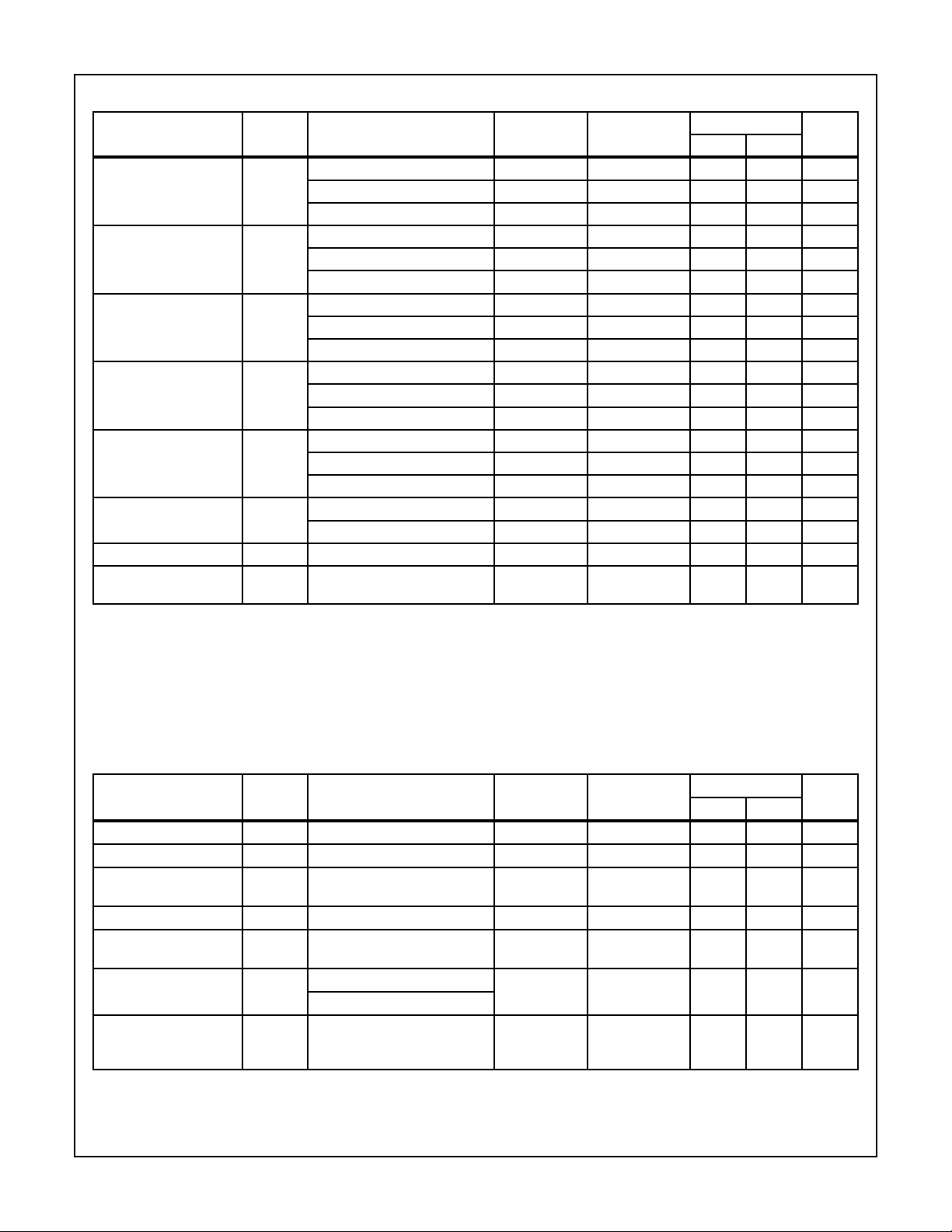
TABLE 4. POST IRRADIATION ELECTRICAL PERFORMANCE CHARACTERISTICS
LIMITS
PARAMETER SYMBOL CONDITIONS NOTES TEMPERATURE
UNITSMIN MAX
Supply Current IDD VDD = 20V, VIN = VDD or GND 1, 4 +25oC-25µA
N Threshold Voltage VNTH VDD = 10V, ISS = -10µA 1, 4 +25oC -2.8 -0.2 V
N Threshold Voltage
∆VTN VDD = 10V, ISS = -10µA 1, 4 +25oC-±1V
Delta
P Threshold Voltage VTP VSS = 0V, IDD = 10µA 1, 4 +25oC 0.2 2.8 V
P Threshold Voltage
∆VTP VSS = 0V, IDD = 10µA 1, 4 +25oC-±1V
Delta
Functional F VDD = 18V, VIN = VDD or GND 1 +25oC VOH >
VDD/2
Propagation Delay Time TPHL
VDD = 3V, VIN = VDD or GND
VDD = 5V 1, 2, 3, 4 +25oC - 1.35 x
TPLH
VOL <
VDD/2
ns
+25oC
Limit
NOTES: 1. All voltages referenced to device GND.
2. CL = 50pF, RL = 200K, Input TR, TF < 20ns.
3. See Table 2 for +25oC limit.
4. Read and Record
7-915
V
 Loading...