Intersil Corporation CD4042BMS Datasheet

CD4042BMS
December 1992
Features
• High-Voltage Type (20V Rating)
• Clock Polarity Control
• Q and
Q Outputs
• Common Clock
• Low Power TTL Compatible
• Standardized Symmetrical Output Characteristics
• 100% Tested for Quiescent Current at 20V
• Maximum Input Current of 1µA at 18V Over Full Pack-
age Temperature Range; 100nA at 18V and +25
• 5V, 10V and 15V Parametric Ratings
• Noise Margin (Over Full Package T emperature Range):
- 1V at VDD = 5V
- 2V at VDD = 10V
- 2.5V at VDD = 15V
• Meets All Requirements of JEDEC Tentative Standard
No. 13B, “Standard Specifications for Description of
‘B’ Series CMOS Devices”
Applications
• Buffer Storage
• Holding Register
• General Digital Logic
Description
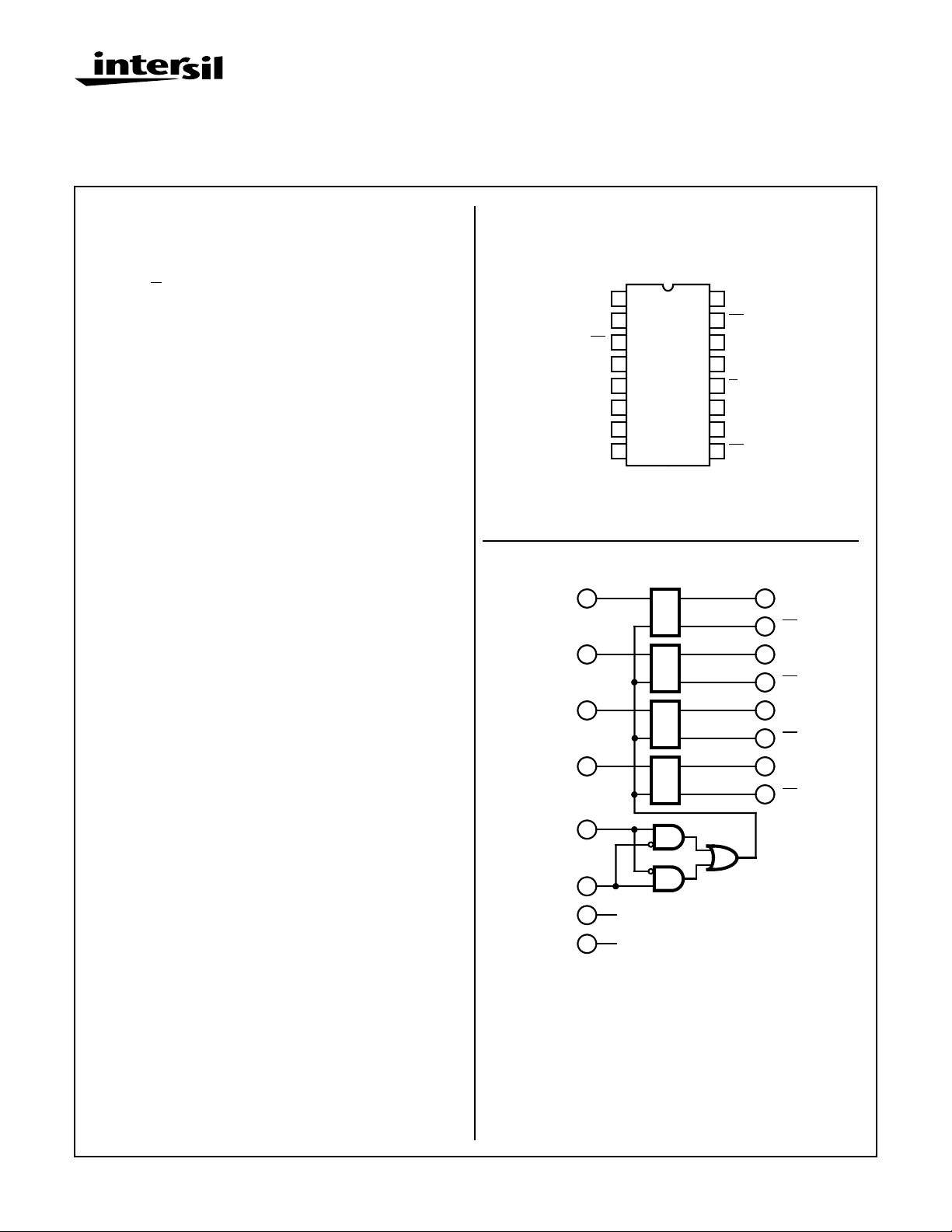
CD4042BMS types contain four latch circuits, each strobed by a
common clock. Complementary buffered outputs are available
from each circuit. The impedance of the n- and p- channel output
devices is balanced and all outputs are electrically identical.
Information present at the data input is transferred to outputs Q
and Q during the CLOCK level which is programmed by the
POLARITY input. For POLARITY = 0 the transfer occurs during
the 0 CLOCK level and for POLARITY = 1 the transfer occurs
during the 1 CLOCK level. The outputs follow the data input
defined above are present. When a CLOCK transition occurs
(positive for POLARITY = 0 and negative for POLARITY = 1) the
information present at the input during the CLOCK transition is
retained at the outputs until an opposite CLOCK transition
occurs.
CMOS Quad Clocked “D” Latch
Pinout
CD4042BMS
TOP VIEW
16
1
Q4
2
Q1
3
Q1
4
D1
D2
VSS
5
6
7
8
CLOCK
POLARITY
o
C
NC = NO CONNECTION
Functional Diagram
D1
4
D2
7
D3
13
D4
14
CLOCK
5
POLARITY
6
VDD
16
VSS
8
VDD
15
Q4
D4
14
D3
13
12
Q3
Q3
11
Q2
10
9
Q2
Q1
2
Q1
3
Q2
10
Q2
9
Q3
11
Q3
12
Q4
1
15
Q4
CL
The CD4042BMS is supplied in these 16 lead outline packages:
Braze Seal DIP H4T
Frit Seal DIP H1E
Ceramic Flatpack H6W
CAUTION: These devices are sensitive to electrostatic discharge; follow proper IC Handling Procedures.
1-888-INTERSIL or 321-724-7143 | Copyright © Intersil Corporation 1999
7-868
File Number
3310

Specifications CD4042BMS
Absolute Maximum Ratings Reliability Information
DC Supply Voltage Range, (VDD) . . . . . . . . . . . . . . . -0.5V to +20V
(Voltage Referenced to VSS Terminals)
Input Voltage Range, All Inputs . . . . . . . . . . . . .-0.5V to VDD +0.5V
DC Input Current, Any One Input . . . . . . . . . . . . . . . . . . . . . . . .±10mA
Operating Temperature Range. . . . . . . . . . . . . . . . -55
Package Types D, F, K, H
Storage Temperature Range (TSTG). . . . . . . . . . . -65
o
C to +125oC
o
C to +150oC
Lead Temperature (During Soldering) . . . . . . . . . . . . . . . . . +265
At Distance 1/16 ± 1/32 Inch (1.59mm ± 0.79mm) from case for
10s Maximum
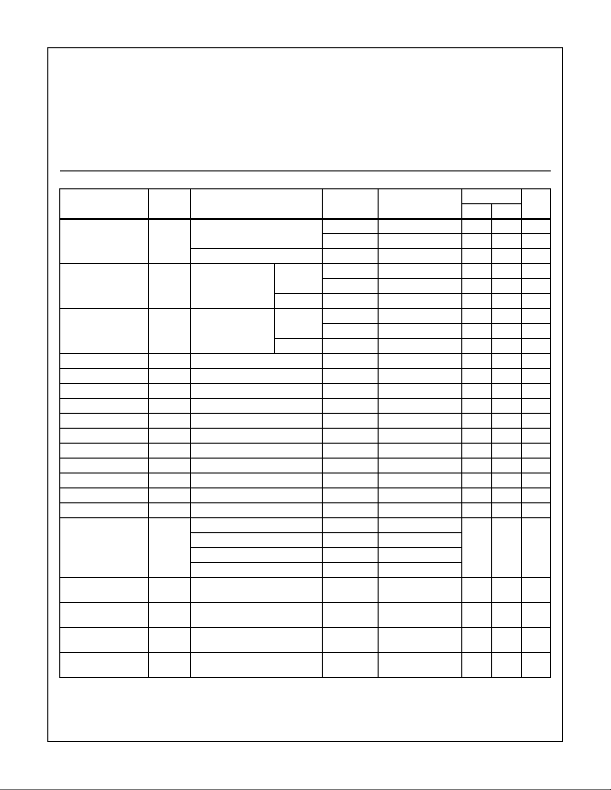
TABLE 1. DC ELECTRICAL PERFORMANCE CHARACTERISTICS
PARAMETER SYMBOL CONDITIONS (NOTE 1)
Supply Current IDD VDD = 20V, VIN = VDD or GND 1 +25
VDD = 18V, VIN = VDD or GND 3 -55oC-2µA
Input Leakage Current IIL VIN = VDD or GND VDD = 20 1 +25
VDD = 18V 3 -55oC -100 - nA
Input Leakage Current IIH VIN = VDD or GND VDD = 20 1 +25oC - 100 nA
VDD = 18V 3 -55oC - 100 nA
Output Voltage VOL15 VDD = 15V, No Load 1, 2, 3 +25oC, +125oC, -55oC - 50 mV
Output Voltage VOH15 VDD = 15V, No Load (Note 3) 1, 2, 3 +25oC, +125oC, -55oC 14.95 - V
Output Current (Sink) IOL5 VDD = 5V, VOUT = 0.4V 1 +25oC 0.53 - mA
Output Current (Sink) IOL10 VDD = 10V, VOUT = 0.5V 1 +25oC 1.4 - mA
Output Current (Sink) IOL15 VDD = 15V, VOUT = 1.5V 1 +25oC 3.5 - mA
Output Current (Source) IOH5A VDD = 5V, VOUT = 4.6V 1 +25oC - -0.53 mA
Output Current (Source) IOH5B VDD = 5V, VOUT = 2.5V 1 +25oC - -1.8 mA
Output Current (Source) IOH10 VDD = 10V, VOUT = 9.5V 1 +25oC - -1.4 mA
Output Current (Source) IOH15 VDD = 15V, VOUT = 13.5V 1 +25oC - -3.5 mA
N Threshold Voltage VNTH VDD = 10V, ISS = -10µA 1 +25oC -2.8 -0.7 V
P Threshold Voltage VPTH VSS = 0V, IDD = 10µA 1 +25oC 0.7 2.8 V
Functional F VDD = 2.8V, VIN = VDD or GND 7 +25oC VOH >
VDD = 20V, VIN = VDD or GND 7 +25oC
VDD = 18V, VIN = VDD or GND 8A +125oC
VDD = 3V, VIN = VDD or GND 8B -55oC
Input Voltage Low
VIL VDD = 5V, VOH > 4.5V, VOL < 0.5V 1, 2, 3 +25oC, +125oC, -55oC - 1.5 V
(Note 2)
Input Voltage High
VIH VDD = 5V, VOH > 4.5V, VOL < 0.5V 1, 2, 3 +25oC, +125oC, -55oC 3.5 - V
(Note 2)
Input Voltage Low
(Note 2)
Input Voltage High
(Note 2)
VIL VDD = 15V, VOH > 13.5V,
VOL < 1.5V
VIH VDD = 15V, VOH > 13.5V,
VOL < 1.5V
NOTES: 1. All voltages referenced to device GND.
2. Go/no go test with limits applied to inputs.
Thermal Resistance . . . . . . . . . . . . . . . . θ
Ceramic DIP Package. . . . . . . . . . . . . 80oC/W 20oC/W
Flatpack Package . . . . . . . . . . . . . . . . 70
Maximum Package Power Dissipation (PD) at +125oC
For TA = -55
For TA = +100
o
C
Device Dissipation per Output Transistor . . . . . . . . . . . . . . . 100mW
o
C to +100oC (Package Type D, F, K). . . . . . 500mW
o
C to +125oC (Package Type D, F, K) . . . . .Derate
Linearity at 12mW/oC to 200mW
ja
o
C/W 20oC/W
For TA = Full Package Temperature Range (All Package Types)
Junction Temperature . . . . . . . . . . . . . . . . . . . . . . . . . . . . . . +175oC
GROUP A
LIMITS
SUBGROUPS TEMPERATURE
o
C-2µA
2 +125oC - 200 µA
o
C -100 - nA
2 +125oC -1000 - nA
2 +125oC - 1000 nA
VOL <
VDD/2
VDD/2
1, 2, 3 +25oC, +125oC, -55oC- 4 V
1, 2, 3 +25oC, +125oC, -55oC11 - V
3. For accuracy, voltage is measured differentially to VDD. Limit
is 0.050V max.
θ
jc
UNITSMIN MAX
V
7-869

Specifications CD4042BMS
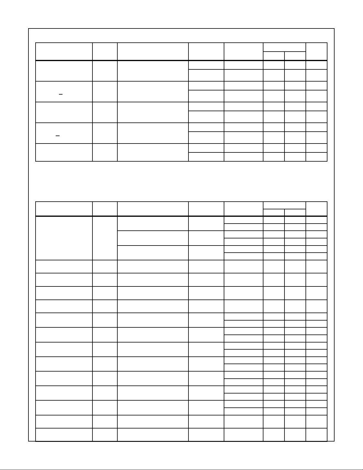
TABLE 2. AC ELECTRICAL PERFORMANCE CHARACTERISTICS
PARAMETER SYMBOL CONDITIONS (NOTES 1, 2)
Propagation Delay
(Note 2)
Data in to Q
Propagation Delay
(Note 2)
Data in to Q
Propagation Delay
(Note 2)
Clock to Q
Propagation Delay
(Note 2)
Clock to Q
Transition Time
(Note 2)
NOTES:
1. VDD = 5V, CL = 50pF, RL = 200K, input TR, TF < 20ns.
2. -55oC and +125oC limits guaranteed, 100% testing being implemented.
TPHL1
TPLH1
TPHL2
TPLH2
TPHL3
TPLH3
TPHL4
TPLH4
TTHL
TTLH
VDD = 5V, VIN = VDD or GND 9 +25oC - 220 ns
VDD = 5V, VIN = VDD or GND 9 +25oC - 300 ns
VDD = 5V, VIN = VDD or GND 9 +25oC - 450 ns
VDD = 5V, VIN = VDD or GND 9 +25oC - 500 ns
VDD = 5V, VIN = VDD or GND 9 +25oC - 200 ns
GROUP A
SUBGROUPS TEMPERATURE
10, 11 +125oC, -55oC - 297 ns
10, 11 +125oC, -55oC - 405 ns
10, 11 +125oC, -55oC - 608 ns
10, 11 +125oC, -55oC - 675 ns
10, 11 +125oC, -55oC - 270 ns
LIMITS
UNITSMIN MAX
TABLE 3. ELECTRICAL PERFORMANCE CHARACTERISTICS
LIMITS
PARAMETER SYMBOL CONDITIONS NOTES TEMPERATURE
Supply Current IDD VDD = 5V, VIN = VDD or GND 1, 2 -55oC, +25oC- 1 µA
+125oC-30µA
VDD = 10V, VIN = VDD or GND 1, 2 -55oC, +25oC- 2 µA
+125oC-60µA
VDD = 15V, VIN = VDD or GND 1, 2 -55oC, +25oC- 2 µA
+125oC - 120 µA
Output Voltage VOL VDD = 5V, No Load 1, 2 +25oC, +125oC,
-55oC
Output Voltage VOL VDD = 10V, No Load 1, 2 +25oC, +125oC,
-55oC
Output Voltage VOH VDD = 5V, No Load 1, 2 +25oC, +125oC,
-55oC
Output Voltage VOH VDD = 10V, No Load 1, 2 +25oC, +125oC,
-55oC
Output Current (Sink) IOL5 VDD = 5V, VOUT = 0.4V 1, 2 +125oC 0.36 - mA
-55oC 0.64 - mA
Output Current (Sink) IOL10 VDD = 10V, VOUT = 0.5V 1, 2 +125oC 0.9 - mA
-55oC 1.6 - mA
Output Current (Sink) IOL15 VDD = 15V, VOUT = 1.5V 1, 2 +125oC 2.4 - mA
-55oC 4.2 - mA
Output Current (Source) IOH5A VDD = 5V, VOUT = 4.6V 1, 2 +125oC - -0.36 mA
-55oC - -0.64 mA
Output Current (Source) IOH5B VDD = 5V, VOUT = 2.5V 1, 2 +125oC - -1.15 mA
-55oC - -2.0 mA
Output Current (Source) IOH10 VDD = 10V, VOUT = 9.5V 1, 2 +125oC - -0.9 mA
-55oC - -1.6 mA
Output Current (Source) IOH15 VDD =15V, VOUT = 13.5V 1, 2 +125oC - -2.4 mA
-55oC - -4.2 mA
Input Voltage Low VIL VDD = 10V , VOH > 9V, VOL < 1V 1, 2 +25oC, +125oC,
-55oC
Input Voltage High VIH VDD = 10V, VOH > 9V , VOL < 1V 1, 2 +25oC, +125oC,
-55oC
-50mV
-50mV
4.95 - V
9.95 - V
-3V
+7 - V
UNITSMIN MAX
7-870
 Loading...