7-826
CAUTION: These devices are sensitive to electrostatic discharge; follow proper IC Handling Procedures.
1-888-INTERSIL or 321-724-7143 | Copyright © Intersil Corporation 1999
CD4033BMS
CMOS Decade Counter/Divider
Description
CD4033BMS consists of a 5 stage Johnson decade counter
and an output decoder which converts the Johnson code to a 7
segment decoded output for driving one stage in a numerical
display.
This device is particularly advantageous in display applications
where low power dissipation and/or low package count is
important.
A high RESET signal clears the decade counter to its zero
count. The counter is advanced one count at the positive clock
signal transition if the CLOCK INHIBIT signal is low. Counter
advancement via the clock line is inhibited when the CLOCK
INHIBIT signal is high. The CLOCK INHIBIT signal can be used
as a negative-edge clock if the clock line is held high. Antilock
gating is provided on the JOHNSON counter, thus assuring
proper counting sequence. The CARRY-OUT (Cout) signal
completes one cycle every ten CLOCK INPUT cycles and is
used to clock the succeeding decade directly in a multi-decade
counting chain.
The seven decoded outputs (a, b, c, d, e, f, g) illuminate the
proper segments in a seven segment display device used for
representing the decimal numbers 0 to 9. The 7 segment outputs go high on selection.
Features
• High Voltage Types (20V Rating)
• Decoded 7 Segment Display Outputs and Ripple
Blanking
• Counter and 7 Segment Decoding in One Package
• Easily Interfaced with 7 Segment Display Types
• Fully Static Counter Operation DC to 6MHz (typ.) at VDD =
10V
• Ideal for Low-Power Displays
• “Ripple Blanking” and Lamp Test
• 100% Tested for Quiescent Current at 20V
• Standardized Symmetrical Output Characteristics
• 5V, 10V and 15V Parametric Ratings
• Schmitt-Triggered Clock Inputs
• Meets All Requirements of JEDEC Tentative Standards No. 13B, “Standard Specifications for Description of “B” Series CMOS Device’s
Applications
• Decade Counting 7 Segment Decimal Display
• Frequency Division 7 Segment Decimal Displays
• Clocks, Watches, Timers (e.g. ÷ 60, ÷ 60, ÷12 Counter/
Display
• Counter/Display Driver For Meter Applications
File Number
3301
December 1992
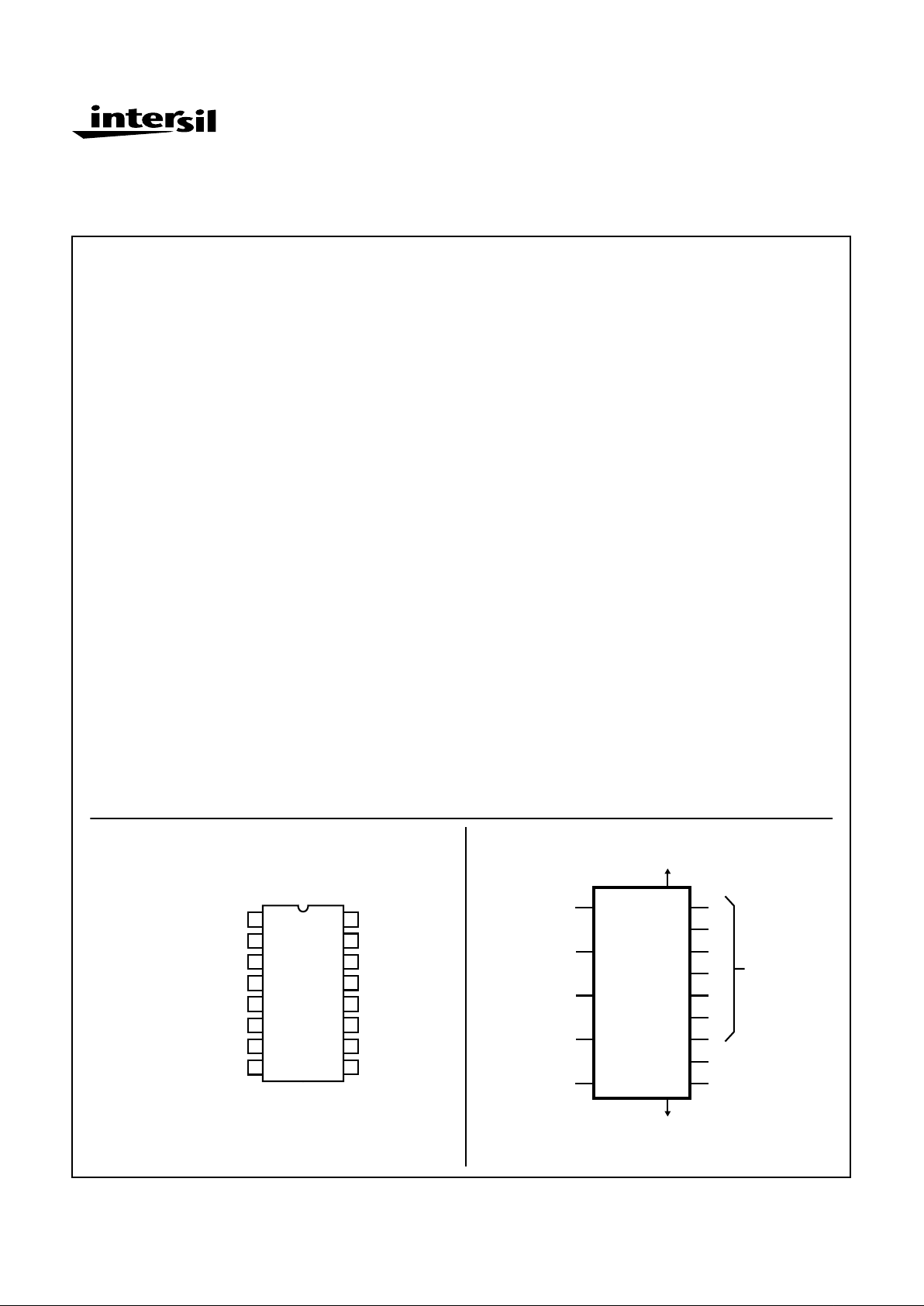
Pinout
CD4033BMS
TOP VIEW
14
15
16
9
13
12
11
10
1
2
3
4
5
7
6
8
CLOCK
CLOCK INHIBIT
RIPPLE BLANKING IN
RIPPLE BLANKING OUT
CARRY OUT
f
VSS
g
VDD
LAMP TEST
c
b
e
a
d
RESET
Functional Diagram
CLOCK
b
c
d
e
f
g
CARRY OUT
RIPPLE
VSS
VDD
110
12
13
9
11
6
7
5
16
8
a
4
7 DECODED OUTPUTS
BLK
OUT
3
RIPPLE
BLK
IN
2
15
CLOCK
INHIBIT
RESET
14
LAMP
TEST

7-827
CD4033BMS
The CD4033BMS has provisions for automatic blanking of
the non-significant zeros in a multi-digit decimal number
which results in an easily readable display consistent with
normal writing practice. For example, the number 0050.0700
in an eight digit display would be displayed as 50.07. Zero
suppression on the integer side is obtained by connecting
the RBI terminal of the CD4033BMS associated with the
most significant digit in the display to a low-level voltage and
connecting the RBO terminal of that stage to the RBI terminal of the CD4033BMS in the next-lower significant position
in the display. This procedure is continued for each succeeding CD4033BMS on the interger side of the display.
On the fraction side of the display the RBI of the
CD4033BMS associated with the least significant bit is connected to a low-level voltage and the RBO of that
CD4033BMS is connected to the RBI terminal of the
CD4033BMS in the next more-significant-bit position. Again,
this procedure is continued for all CD4033BMS’s on the fraction side of the display.
In a purely fractional number the zero immediately preceding
the decimal point can be displayed by connecting the RBI of
that stage to a high level voltage (instead of to the RBO of
the next more-significant-stage). For example: optional zero
→ 0.7346. Likewise, the zero in a number such as 763.0 can
be displayed by connecting the RBI of the CD4033BMS
associated with it to a high-level voltage.
Ripple blanking of non-significant zeros provides an appreciable savings in display power.
The CD4033BMS has a LAMP TEST input which, when connected to a high-level voltage, overrides normal decoder
operation and enables a check to be made on possible display malfunctions by putting the seven outputs in the high
state.
The CD4033BMS are supplied in these 16 lead outline packages:
Braze Seal DIP H4W
Frit Seal DIP H2R
Ceramic Flatpack H6W
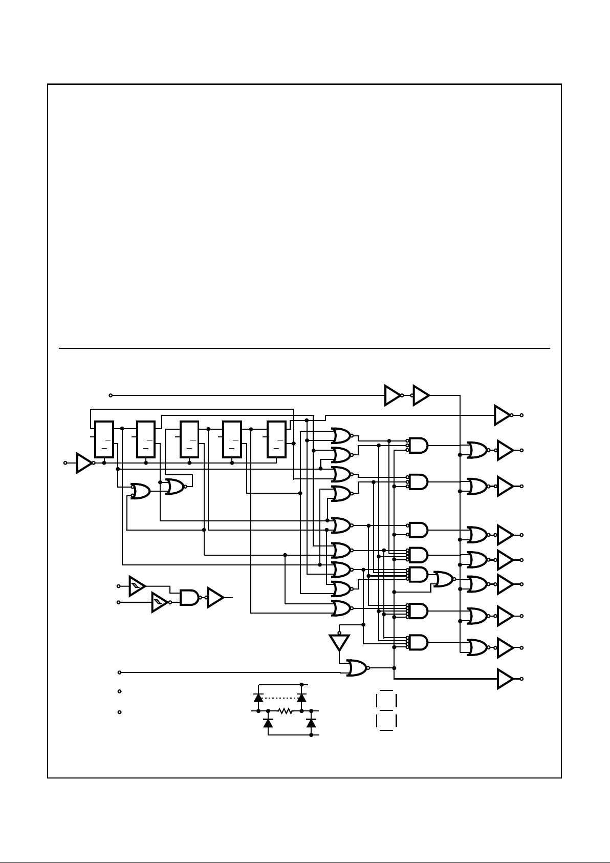
Logic Diagram
FIGURE 1. CD4033BMS
DQ
CL
Q
R
CL
DQ
CL
Q
R
CL
DQ
CL
Q
R
CL
DQ
CL
Q
R
CL
DQ
CL
Q
R
CL
CL
1
2
*CLOCK
*CLOCK
INHIBIT
15
*
RESET
*RBI
3
16
8
VDD
GND
5
COUT
(CLOCK
÷ 10)
4
7
6
11
9
13
12
10
a
b
c
d
e
f
g
VDD
VSS
*ALL INPUTS PROTECTED
BY CMOS INPUT
PROTECTION NETWORK
a
b
c
d
e
f
g
SEGMENT
DESIGNATIONS
14
*LAMP TEST
RBO

7-828
Specifications CD4033BMS
Absolute Maximum Ratings Reliability Information
DC Supply Voltage Range, (VDD) . . . . . . . . . . . . . . . -0.5V to +20V
(Voltage Referenced to VSS Terminals)
Input Voltage Range, All Inputs . . . . . . . . . . . . .-0.5V to VDD +0.5V
DC Input Current, Any One Input . . . . . . . . . . . . . . . . . . . . . . . .±10mA
Operating Temperature Range. . . . . . . . . . . . . . . . -55
o
C to +125oC
Package Types D, F, K, H
Storage Temperature Range (TSTG). . . . . . . . . . . -65
o
C to +150oC
Lead Temperature (During Soldering) . . . . . . . . . . . . . . . . . +265
o
C
At Distance 1/16 ± 1/32 Inch (1.59mm ± 0.79mm) from case for
10s Maximum
Thermal Resistance . . . . . . . . . . . . . . . . θ
ja
θ
jc
Ceramic DIP and FRIT Package. . . . . 80oC/W 20oC/W
Flatpack Package . . . . . . . . . . . . . . . . 70
o
C/W 20oC/W
Maximum Package Power Dissipation (PD) at +125oC
For TA = -55
o
C to +100oC (Package Type D, F, K). . . . . . 500mW
For TA = +100
o
C to +125oC (Package Type D, F, K) . . . . .Derate
Linearity at 12mW/oC to 200mW
Device Dissipation per Output Transistor . . . . . . . . . . . . . . . 100mW
For TA = Full Package Temperature Range (All Package Types)
Junction Temperature . . . . . . . . . . . . . . . . . . . . . . . . . . . . . . +175oC
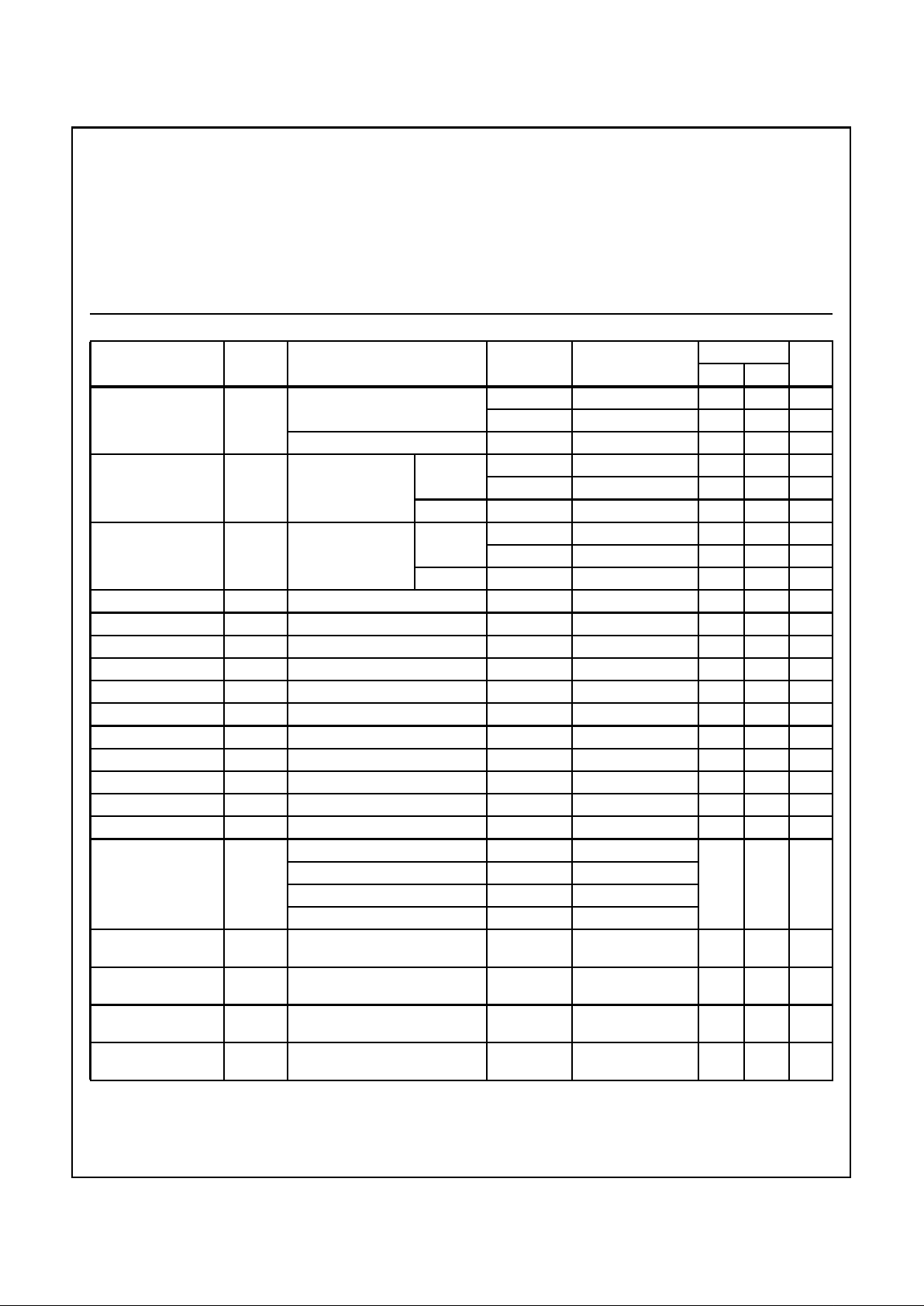
TABLE 1. DC ELECTRICAL PERFORMANCE CHARACTERISTICS
PARAMETER SYMBOL CONDITIONS (NOTE 1)
GROUP A
SUBGROUPS TEMPERATURE
LIMITS
UNITSMIN MAX
Supply Current IDD VDD = 20V, VIN = VDD or GND 1 +25
o
C-10µA
2 +125oC - 1000 µA
VDD = 18V, VIN = VDD or GND 3 -55oC-10µA
Input Leakage Current IIL VIN = VDD or GND VDD = 20 1 +25
o
C -100 - nA
2 +125oC -1000 - nA
VDD = 18V 3 -55oC -100 - nA
Input Leakage Current IIH VIN = VDD or GND VDD = 20 1 +25oC - 100 nA
2 +125oC - 1000 nA
VDD = 18V 3 -55oC - 100 nA
Output Voltage VOL15 VDD = 15V, No Load 1, 2, 3 +25oC, +125oC, -55oC - 50 mV
Output Voltage VOH15 VDD = 15V, No Load (Note 3) 1, 2, 3 +25oC, +125oC, -55oC 14.95 - V
Output Current (Sink) IOL5 VDD = 5V, VOUT = 0.4V 1 +25oC 0.53 - mA
Output Current (Sink) IOL10 VDD = 10V, VOUT = 0.5V 1 +25oC 1.4 - mA
Output Current (Sink) IOL15 VDD = 15V, VOUT = 1.5V 1 +25oC 3.5 - mA
Output Current (Source) IOH5A VDD = 5V, VOUT = 4.6V 1 +25oC - -0.53 mA
Output Current (Source) IOH5B VDD = 5V, VOUT = 2.5V 1 +25oC - -1.8 mA
Output Current (Source) IOH10 VDD = 10V, VOUT = 9.5V 1 +25oC - -1.4 mA
Output Current (Source) IOH15 VDD = 15V, VOUT = 13.5V 1 +25oC - -3.5 mA
N Threshold Voltage VNTH VDD = 10V, ISS = -10µA 1 +25oC -2.8 -0.7 V
P Threshold Voltage VPTH VSS = 0V, IDD = 10µA 1 +25oC 0.7 2.8 V
Functional F VDD = 2.8V, VIN = VDD or GND 7 +25oC VOH >
VDD/2
VOL <
VDD/2
V
VDD = 20V, VIN = VDD or GND 7 +25oC
VDD = 18V, VIN = VDD or GND 8A +125oC
VDD = 3V, VIN = VDD or GND 8B -55oC
Input Voltage Low
(Note 2)
VIL VDD = 5V, VOH > 4.5V, VOL < 0.5V 1, 2, 3 +25oC, +125oC, -55oC - 1.5 V
Input Voltage High
(Note 2)
VIH VDD = 5V, VOH > 4.5V, VOL < 0.5V 1, 2, 3 +25oC, +125oC, -55oC 3.5 - V
Input Voltage Low
(Note 2)
VIL VDD = 15V, VOH > 13.5V,
VOL < 1.5V
1, 2, 3 +25oC, +125oC, -55oC- 4 V
Input Voltage High
(Note 2)
VIH VDD = 15V, VOH > 13.5V,
VOL < 1.5V
1, 2, 3 +25oC, +125oC, -55oC11 - V
NOTES: 1. All voltages referenced to device GND, 100% testing being
implemented.
2. Go/No Go test with limits applied to inputs.
3. For accuracy, voltage is measured differentially to VDD. Limit
is 0.050V max.

7-829
Specifications CD4033BMS
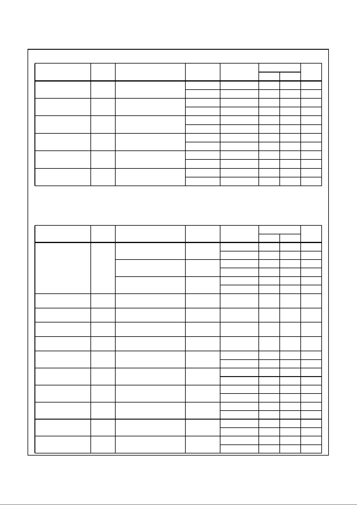
TABLE 2. AC ELECTRICAL PERFORMANCE CHARACTERISTICS
PARAMETER SYMBOL CONDITIONS (NOTE 1, 2)
GROUP A
SUBGROUPS TEMPERATURE
LIMITS
UNITSMIN MAX
Propagation Delay
Clock To Carry Out
TPHL1
TPLH1
VDD = 5V, VIN = VDD or GND 9 +25oC - 500 ns
10, 11 +125oC, -55oC - 675 ns
Propagation Delay
Clock To Decode Out
TPHL2
TPLH2
VDD = 5V, VIN = VDD or GND 9 +25oC - 700 ns
10, 11 +125oC, -55oC - 945 ns
Propagation Delay
Reset To Carry Out
TPLH3 VDD = 5V, VIN = VDD or GND 9 +25oC - 550 ns
10, 11 +125oC, -55oC - 743 ns
Propagation Delay
Reset To Decode Out
TPHL4
TPLH4
VDD = 5V, VIN = VDD or GND 9 +25oC - 600 ns
10, 11 +125oC, -55oC - 810 ns
Transition Time TTHL
TTLH
VDD = 5V, VIN = VDD or GND 9 +25oC - 200 ns
10, 11 +125oC, -55oC - 270 ns
Maximum Clock Input
Frequency
FCL VDD = 5V, VIN = VDD or GND 9 +25oC 2.5 - MHz
10, 11 +125oC, -55oC 1.85 - MHz
NOTES:
1. VDD = 5V, CL = 50pF, RL = 200K
2. -55oC and +125oC limits guaranteed, 100% testing being implemented.
TABLE 3. ELECTRICAL PERFORMANCE CHARACTERISTICS
PARAMETER SYMBOL CONDITIONS NOTES TEMPERATURE
LIMITS
UNITSMIN MAX
Supply Current IDD VDD = 5V, VIN = VDD or GND 1, 2 -55oC, +25oC- 5 µA
+125oC - 150 µA
VDD = 10V, VIN = VDD or GND 1, 2 -55oC, +25oC- 10µA
+125oC - 300 µA
VDD = 15V, VIN = VDD or GND 1, 2 -55oC, +25oC- 10µA
+125oC - 600 µA
Output Voltage VOL VDD = 5V, No Load 1, 2 +25oC, +125oC,
-55oC
-50mV
Output Voltage VOL VDD = 10V, No Load 1, 2 +25oC, +125oC,
-55oC
-50mV
Output Voltage VOH VDD = 5V, No Load 1, 2 +25oC, +125oC,
-55oC
4.95 - V
Output Voltage VOH VDD = 10V, No Load 1, 2 +25oC, +125oC,
-55oC
9.95 - V
Output Current (Sink) IOL5 VDD = 5V, VOUT = 0.4V 1, 2 +125oC 0.36 - mA
-55oC 0.64 - mA
Output Current (Sink) IOL10 VDD = 10V, VOUT = 0.5V 1, 2 +125oC 0.9 - mA
-55oC 1.6 - mA
Output Current (Sink) IOL15 VDD = 15V, VOUT = 1.5V 1, 2 +125oC 2.4 - mA
-55oC 4.2 - mA
Output Current (Source) IOH5A VDD = 5V, VOUT = 4.6V 1, 2 +125oC - -0.36 mA
-55oC - -0.64 mA
Output Current (Source) IOH5B VDD = 5V, VOUT = 2.5V 1, 2 +125oC - -1.15 mA
-55oC - -2.0 mA
Output Current (Source) IOH10 VDD = 10V, VOUT = 9.5V 1, 2 +125oC - -0.9 mA
-55oC - -2.6 mA
 Loading...