Intersil Corporation CD4029BMS Datasheet

CD4029BMS
December 1992
Features
• High-Voltage Type (20V Rating)
• Medium Speed Operation: 8MHz (Typ.) at CL = 50pF
and VDD - VSS = 10V
• Multi-Package Parallel Clocking for Synchronous High
Speed Output Response or Ripple Clocking for Slow
Clock Input Rise and Fall Times
• “Preset Enable” and Individual “Jam” Inputs Provided
• Binary or Decade Up/Down Counting
• BCD Outputs in Decade Mode
• 100% Tested for Maximum Quiescent Current at 20V
• 5V, 10V and 15V Parametric Ratings
• Standardized Symmetrical Output Characteristics
• Maximum Input Current of 1µA at 18V Over Full Package-Temperature Range; 100nA at 18V and +25
• Noise Margin (Over Full Package T emperature Range):
- 1V at VDD = 5V
- 2V at VDD = 10V
- 2.5V at VDD = 15V
• Meets All Requirements of JEDEC Tentative Standards No. 13B, “Standard Specifications for Description of “B” Series CMOS Device’s
Applications
• Programmable Binary and Decade Counting/Frequency Synthesizers-BCD Output
• Analog to Digital and Digital to Analog Conversion
• Up/Down Binary Counting
• Difference Counting
• Magnitude and Sign Generation
• Up/Down Decade Counting
CMOS Presettable Up/Down Counter
Description
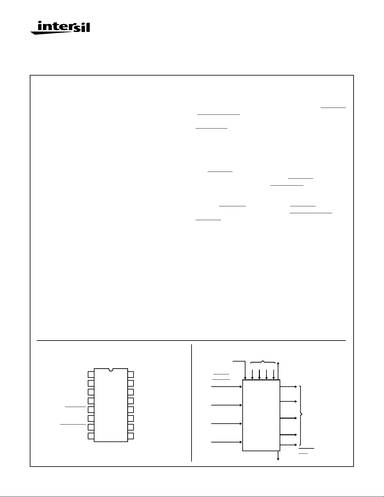
CD4029BMS consists of a four-stage binary or BCD-decade up/
down counter with provisions for look-ahead carry in both counting modes. The inputs consist of a single CLOCK,
(
CLOCK ENABLE), BINARY/DECADE, UP/DOWN, PRESET
ENABLE, and four individual JAM signals. Q1, Q2, Q3, Q4 and a
CARRY OUT signal are provided as outputs.
A high PRESET ENABLE signal allows information on the JAM
INPUTS to preset the counter to any state asynchronously with
the clock. A low on each JAM line, when the PRESET-ENABLE
signal is high, resets the counter to its zero count. The counter is
advanced one count at the positive transition of the clock when
the
CARRY-IN and PRE-SET ENABLE signals are low.
Advancement is inhibited when the
ENABLE signals are high. The
o
C
high and goes low when the counter reaches its maximum count
in the UP mode or the minimum count in the DOWN mode provided the
CARRY-I N signal is low. The CARRY-IN signal in the
low state can thus be considered a
CARRY-IN or PRESET
CARRY-OUT signal is normally
CLOCK ENABLE. The
CARRY-IN terminal must be connected to VSS when not in use.
Binary counting is accomplished when the BINARY/DECADE
input is high; the counter counts in the decade mode when the
BINARY/DECADE input is low . The counter counts up when the
UP/DOWN input is high, and down when the UP/DOWN input is
low. Multiple packages can be connected in either a parallelclocking or a ripple-clocking arrangement as shown in Figure 17.
Parallel clocking provides synchronous control and hence faster
response from all counting outputs. Ripple-clocking allows for
longer clock input rise and fall times.
The CD4029BMS is supplied in these 16-lead outline packages:
Braze Seal DIP H4X
Frit Seal DIP H1F
Ceramic Flatpack H6W
CARRY-IN
Pinout
CD4029BMS
TOP VIEW
VDD
16
CLOCK
15
Q3
14
JAM 3
13
JAM 2
12
Q2
11
UP/DOWN
10
BINARY/DECADE
9
Q4
JAM 4
JAM 1
Q1
VSS
1
2
3
4
5
6
7
8
PRESET ENABLE
CARRY IN
CARRY OUT
CAUTION: These devices are sensitive to electrostatic discharge; follow proper IC Handling Procedures.
1-888-INTERSIL or 321-724-7143 | Copyright © Intersil Corporation 1999
Functional Diagram
PRESET
ENABLE
CARRY IN
(
CLOCK
ENABLE)
BINARY/
DECADE
UP/DOWN
CLOCK
7-798
JAM INPUTS
1234
14 3
5
9
10
15
1312 16
VDD
6
11
14
2
7
8
VSS
Q1
Q2
Q3
Q4
CARRY
OUT
File Number
BUFFERED
OUTPUTS
3304

Specifications CD4029BMS
Absolute Maximum Ratings Reliability Information
DC Supply Voltage Range, (VDD) . . . . . . . . . . . . . . . -0.5V to +20V
(Voltage Referenced to VSS Terminals)
Input Voltage Range, All Inputs . . . . . . . . . . . . .-0.5V to VDD +0.5V
DC Input Current, Any One Input . . . . . . . . . . . . . . . . . . . . . . . .±10mA
Operating Temperature Range. . . . . . . . . . . . . . . . -55
Package Types D, F, K, H
Storage Temperature Range (TSTG) . . . . . . . . . . . -65
o
C to +125oC
o
C to +150oC
Lead Temperature (During Soldering) . . . . . . . . . . . . . . . . . +265
At Distance 1/16 ± 1/32 Inch (1.59mm ± 0.79mm) from case for
10s Maximum
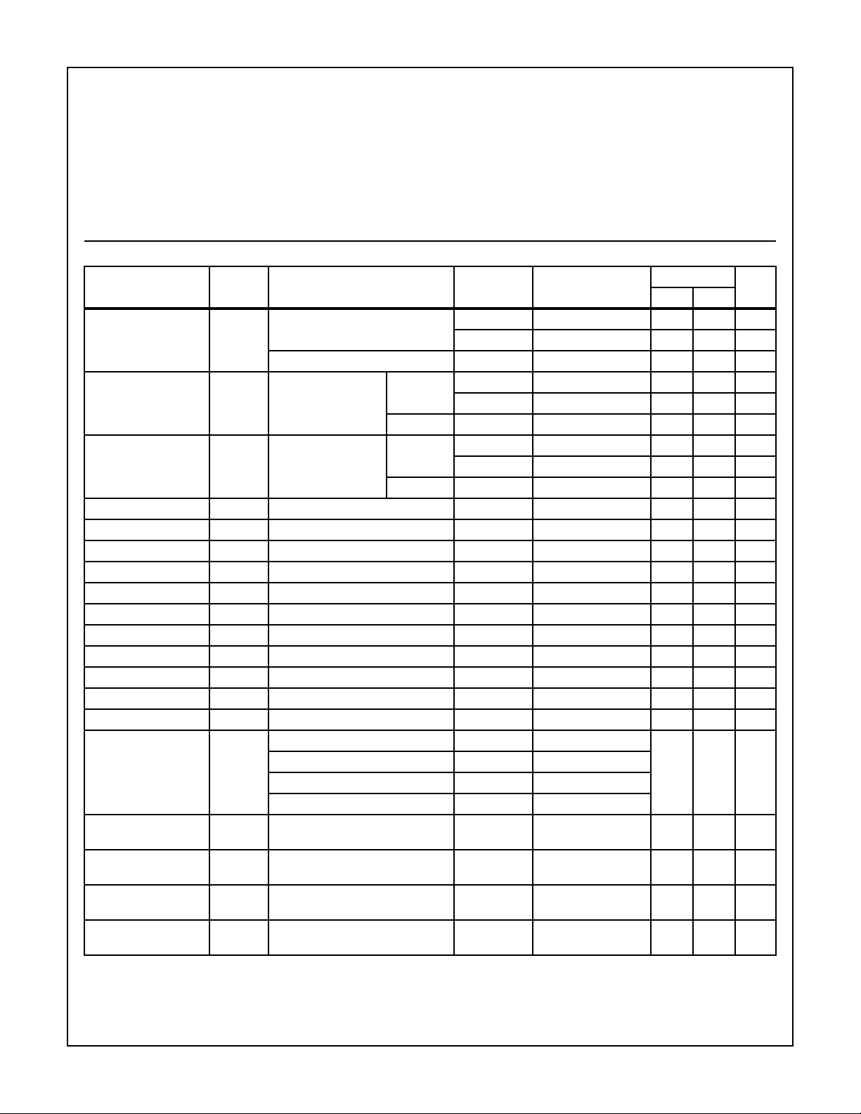
TABLE 1. DC ELECTRICAL PERFORMANCE CHARACTERISTICS
PARAMETER SYMBOL CONDITIONS (NOTE 1)
Supply Current IDD VDD = 20V, VIN = VDD or GND 1 +25
VDD = 18V, VIN = VDD or GND 3 -55oC-10µA
Input Leakage Current IIL VIN = VDD or GND VDD = 20 1 +25
VDD = 18V 3 -55oC -100 - nA
Input Leakage Current IIH VIN = VDD or GND VDD = 20 1 +25oC - 100 nA
VDD = 18V 3 -55oC - 100 nA
Output Voltage VOL15 VDD = 15V, No Load 1, 2, 3 +25oC, +125oC, -55oC - 50 mV
Output Voltage VOH15 VDD = 15V, No Load (Note 3) 1, 2, 3 +25oC, +125oC, -55oC 14.95 - V
Output Current (Sink) IOL5 VDD = 5V, VOUT = 0.4V 1 +25oC 0.53 - mA
Output Current (Sink) IOL10 VDD = 10V, VOUT = 0.5V 1 +25oC 1.4 - mA
Output Current (Sink) IOL15 VDD = 15V, VOUT = 1.5V 1 +25oC 3.5 - mA
Output Current (Source) IOH5A VDD = 5V, VOUT = 4.6V 1 +25oC - -0.53 mA
Output Current (Source) IOH5B VDD = 5V, VOUT = 2.5V 1 +25oC - -1.8 mA
Output Current (Source) IOH10 VDD = 10V, VOUT = 9.5V 1 +25oC - -1.4 mA
Output Current (Source) IOH15 VDD = 15V, VOUT = 13.5V 1 +25oC - -3.5 mA
N Threshold Voltage VNTH VDD = 10V, ISS = -10µA 1 +25oC -2.8 -0.7 V
P Threshold Voltage VPTH VSS = 0V, IDD = 10µA 1 +25oC 0.7 2.8 V
Functional F VDD = 2.8V, VIN = VDD or GND 7 +25oC VOH >
VDD = 20V, VIN = VDD or GND 7 +25oC
VDD = 18V, VIN = VDD or GND 8A +125oC
VDD = 3V, VIN = VDD or GND 8B -55oC
Input Voltage Low
VIL VDD = 5V, VOH > 4.5V, VOL < 0.5V 1, 2, 3 +25oC, +125oC, -55oC - 1.5 V
(Note 2)
Input Voltage High
VIH VDD = 5V, VOH > 4.5V, VOL < 0.5V 1, 2, 3 +25oC, +125oC, -55oC 3.5 - V
(Note 2)
Input Voltage Low
(Note 2)
Input Voltage High
(Note 2)
VIL VDD = 15V, VOH > 13.5V,
VOL < 1.5V
VIH VDD = 15V, VOH > 13.5V,
VOL < 1.5V
NOTES: 1. All voltages referenced to device GND, 100% testing being
implemented.
2. Go/No Go test with limits applied to inputs.
Thermal Resistance . . . . . . . . . . . . . . . . θ
Ceramic DIP and FRIT Package. . . . . 80oC/W 20oC/W
Flatpack Package . . . . . . . . . . . . . . . . 70
Maximum Package Power Dissipation (PD) at +125oC
For TA = -55
For TA = +100
o
C
Device Dissipation per Output Transistor . . . . . . . . . . . . . . . 100mW
o
C to +100oC (Package Type D, F, K). . . . . . 500mW
o
C to +125oC (Package Type D, F, K) . . . . .Derate
Linearity at 12mW/oC to 200mW
ja
o
C/W 20oC/W
For TA = Full Package Temperature Range (All Package Types)
Junction Temperature . . . . . . . . . . . . . . . . . . . . . . . . . . . . . . +175oC
GROUP A
LIMITS
SUBGROUPS TEMPERATURE
o
C-10µA
2 +125oC - 1000 µA
o
C -100 - nA
2 +125oC -1000 - nA
2 +125oC - 1000 nA
VOL <
VDD/2
VDD/2
1, 2, 3 +25oC, +125oC, -55oC- 4 V
1, 2, 3 +25oC, +125oC, -55oC11 - V
3. For accuracy, voltage is measured differentially to VDD. Limit
is 0.050V max.
θ
jc
UNITSMIN MAX
V
7-799

Specifications CD4029BMS
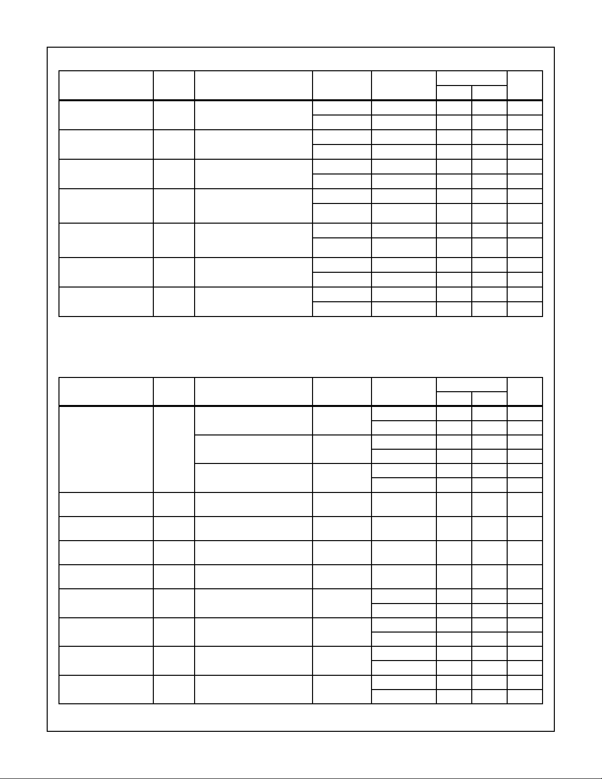
TABLE 2. AC ELECTRICAL PERFORMANCE CHARACTERISTICS
PARAMETER SYMBOL CONDITIONS (NOTE 1, 2)
Propagation Delay
Clock To Q Output
Propagation Delay
Clock To Carry Out
Propagation Delay
Preset Enable To Q
Propagation Delay
Preset Enable To CarryOut
Propagation Delay
Carry-In To
Carry-Out
Transition Time
Q Output
Maximum Clock Input
Frequency
NOTES:
1. VDD = 5V, CL = 50pF, RL = 200K
2. -55oC and +125oC limits guaranteed, 100% testing being implemented.
TPHL1
TPLH1
TPHL2
TPLH2
TPHL3
TPLH3
TPHL4
TPLH4
TPHL5
TPLH5
TTHL
TTLH
FCL VDD = 5V, VIN = VDD or GND 9 +25oC 2 - MHz
VDD = 5V, VIN = VDD or GND 9 +25oC - 500 ns
VDD = 5V, VIN = VDD or GND 9 +25oC - 560 ns
VDD = 5V, VIN = VDD or GND 9 +25oC - 470 ns
VDD = 5V, VIN = VDD or GND 9 +25oC - 640 ns
VDD = 5V, VIN = VDD or GND 9 +25oC - 340 ns
VDD = 5V, VIN = VDD or GND 9 +25oC - 200 ns
GROUP A
SUBGROUPS TEMPERATURE
10, 11 +125oC, -55oC - 675 ns
10, 11 +125oC, -55oC - 756 ns
10, 11 +125oC, -55oC - 635 ns
10, 11 +125oC, -55oC - 864 ns
10, 11 +125oC, -55oC - 459 ns
10, 11 +125oC, -55oC - 270 ns
10, 11 +125oC, -55oC 1.48 - MHz
LIMITS
UNITSMIN MAX
TABLE 3. ELECTRICAL PERFORMANCE CHARACTERISTICS
LIMITS
PARAMETER SYMBOL CONDITIONS NOTES TEMPERATURE
Supply Current IDD VDD = 5V, VIN = VDD or GND 1, 2 -55oC, +25oC- 5 µA
+125oC - 150 µA
VDD = 10V, VIN = VDD or GND 1, 2 -55oC, +25oC- 10µA
+125oC - 300 µA
VDD = 15V, VIN = VDD or GND 1, 2 -55oC, +25oC- 10µA
+125oC - 600 µA
Output Voltage VOL VDD = 5V, No Load 1, 2 +25oC, +125oC,
-55oC
Output Voltage VOL VDD = 10V, No Load 1, 2 +25oC, +125oC,
-55oC
Output Voltage VOH VDD = 5V, No Load 1, 2 +25oC, +125oC,
-55oC
Output Voltage VOH VDD = 10V, No Load 1, 2 +25oC, +125oC,
-55oC
Output Current (Sink) IOL5 VDD = 5V, VOUT = 0.4V 1, 2 +125oC 0.36 - mA
-55oC 0.64 - mA
Output Current (Sink) IOL10 VDD = 10V, VOUT = 0.5V 1, 2 +125oC 0.9 - mA
-55oC 1.6 - mA
Output Current (Sink) IOL15 VDD = 15V, VOUT = 1.5V 1, 2 +125oC 2.4 - mA
-55oC 4.2 - mA
Output Current (Source) IOH5A VDD = 5V, VOUT = 4.6V 1, 2 +125oC - -0.36 mA
-55oC - -0.64 mA
-50mV
-50mV
4.95 - V
9.95 - V
UNITSMIN MAX
7-800

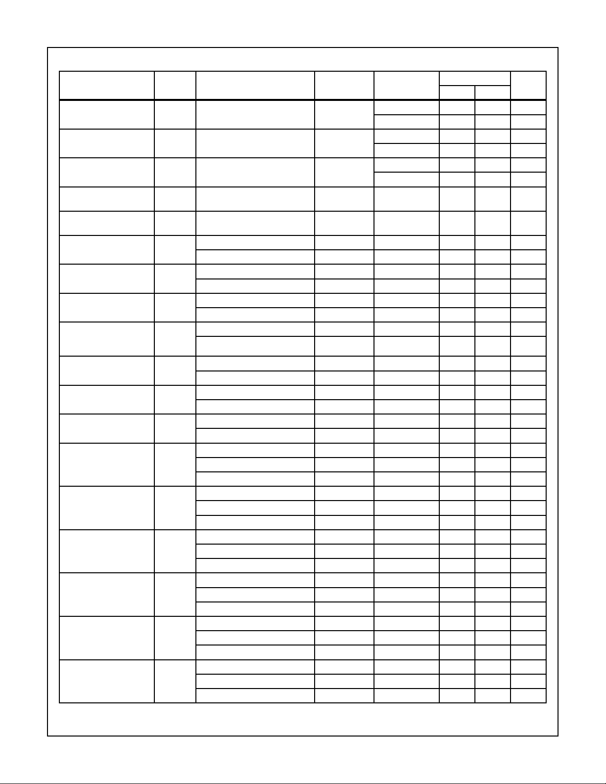
Specifications CD4029BMS
TABLE 3. ELECTRICAL PERFORMANCE CHARACTERISTICS (Continued)
LIMITS
PARAMETER SYMBOL CONDITIONS NOTES TEMPERATURE
Output Current (Source) IOH5B VDD = 5V, VOUT = 2.5V 1, 2 +125oC - -1.15 mA
-55oC - -2.0 mA
Output Current (Source) IOH10 VDD = 10V, VOUT = 9.5V 1, 2 +125oC - -0.9 mA
o
C - -2.6 mA
-55
Output Current (Source) IOH15 VDD =15V, VOUT = 13.5V 1, 2 +125
o
C - -2.4 mA
-55oC - -4.2 mA
o
Input Voltage Low VIL VDD = 10V, VOH > 9V , VOL < 1V 1, 2 +25
Input Voltage High VIH VDD = 10V, VOH > 9V, VOL < 1V 1, 2 +25oC, +125oC,
C, +125oC,
o
-55
C
-3V
7-V
-55oC
o
Propagation Delay
Q Output
Propagation Delay
Carry Output
Propagation Delay
Preset Enable To Q
Propagation Delay
Preset Enable To Carry-
TPHL1
TPLH1
TPHL2
TPLH2
TPHL3
TPLH3
TPHL4
TPLH4
Out
Propagation Delay
Carry In To Carry Out
TPHL5
TPLH5
Transition Time TTHL
TTLH
Maximum Clock Input
FCL VDD = 10V 1, 2, 3 +25oC 4 - MHz
Frequency
Minimum Data Setup
TS VDD = 5V 1, 2, 3 +25oC - 340 ns
Time
Note 4
VDD = 10V 1, 2, 3 +25
VDD = 15V 1, 2, 3 +25
VDD = 10V 1, 2, 3 +25oC - 260 ns
VDD = 15V 1, 2, 3 +25oC - 190 ns
VDD = 10V 1, 2, 3 +25oC - 200 ns
VDD = 15V 1, 2, 3 +25oC - 160 ns
VDD = 10V 1, 2, 3 +25oC - 290 ns
VDD = 15V 1, 2, 3 +25oC - 210 ns
VDD = 10V 1, 2, 3 +25oC - 140 ns
VDD = 15V 1, 2, 3 +25oC - 100 ns
VDD = 10V 1, 2, 3 +25oC - 100 ns
VDD = 15V 1, 2, 3 +25oC - 80 ns
VDD = 15V 1, 2, 3 +25oC 5.5 - MHz
VDD = 10V 1, 2, 3 +25oC - 140 ns
C - 240 ns
o
C - 180 ns
VDD = 15V 1, 2, 3 +25oC - 100 ns
Clock Rise And Fall Time
Note 5
TRCL
TFCL
VDD = 5V 1, 2, 3 +25oC-15µs
VDD = 10V 1, 2, 3 +25oC-15µs
VDD = 15V 1, 2, 3 +25oC-15µs
Minimum Clock Pulse
Width
TW VDD = 5V 1, 2, 3 +25oC - 180 ns
VDD = 10V 1, 2, 3 +25oC - 90 ns
VDD = 15V 1, 2, 3 +25oC - 60 ns
Minimum Carry In Setup
Time
Note 6
TS VDD = 5V 1, 2, 3 +25oC - 200 ns
VDD = 10V 1, 2, 3 +25oC - 70 ns
VDD = 15V 1, 2, 3 +25oC - 60 ns
Minimum Carry Input
Hold Time
Note 6
TH VDD = 5V 1, 2, 3 +25oC - 50 ns
VDD = 10V 1, 2, 3 +25oC - 30 ns
VDD = 15V 1, 2, 3 +25oC - 25 ns
Minimum Preset Enable
Removal Time
Note 4
TREM VDD = 5V 1, 2, 3 +25oC - 200 ns
VDD = 10V 1, 2, 3 +25oC - 110 ns
VDD = 15V 1, 2, 3 +25oC - 80 ns
UNITSMIN MAX
7-801
 Loading...