Intersil Corporation CD4023BMS, CD4011BMS, CD4012BMS Datasheet

CD4011BMS, CD4012BMS
CD4023BMS
November 1994
Features
• High-Voltage Types (20V Rating)
• Propagation Delay Time = 60ns (typ.) at CL = 50pF,
VDD = 10V
• Buffered Inputs and Outputs
• Standardized Symmetrical Output Characteristics
• Maximum Input Current of 1µA at 18V Over Full PackageT emperature Range; 100nA at 18V and +25oC
• 100% Tested for Maximum Quiescent Current at 20V
• 5V, 10V and 15V Parametric Ratings
• Noise Margin (Over Full Package T emperature Range):
- 1V at VDD = 5V
- 2V at VDD = 10V
- 2.5V at VDD = 15V
• Meets All Requirements of JEDEC Tentative Standards No. 13B, “Standard Specifications for Description of “B” Series CMOS Device’s
Description
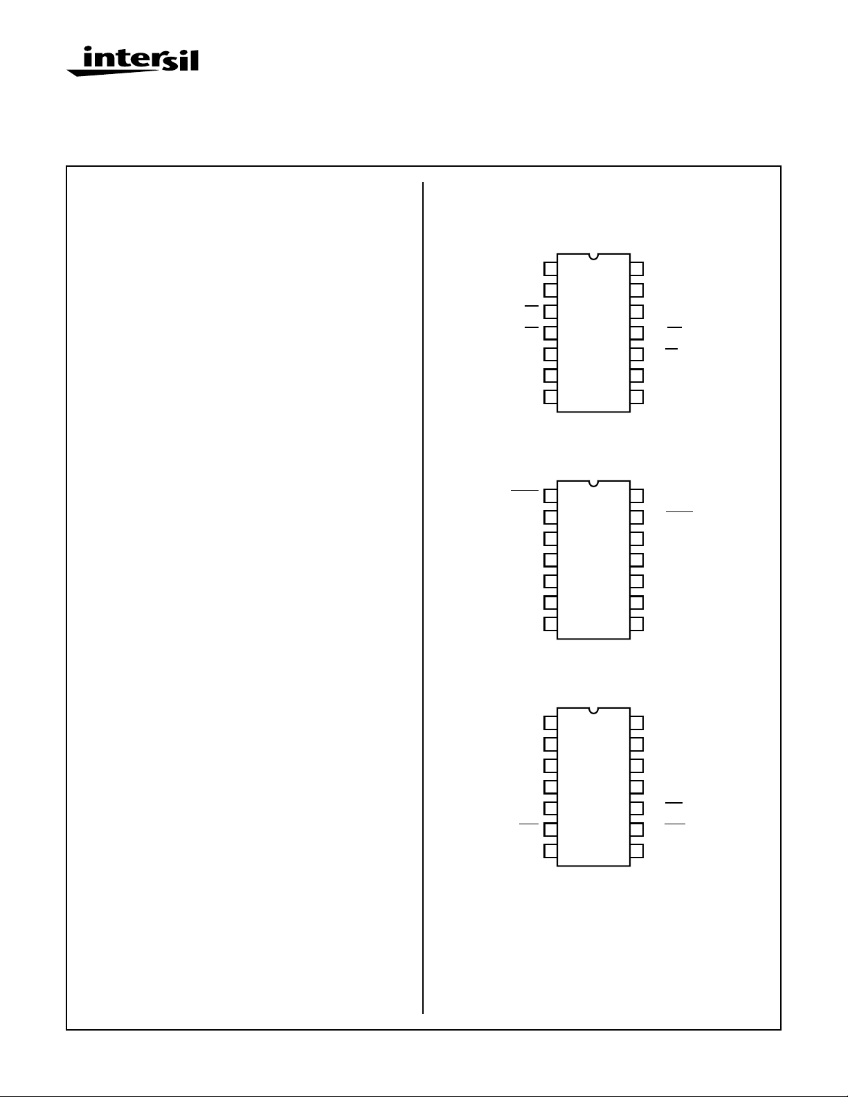
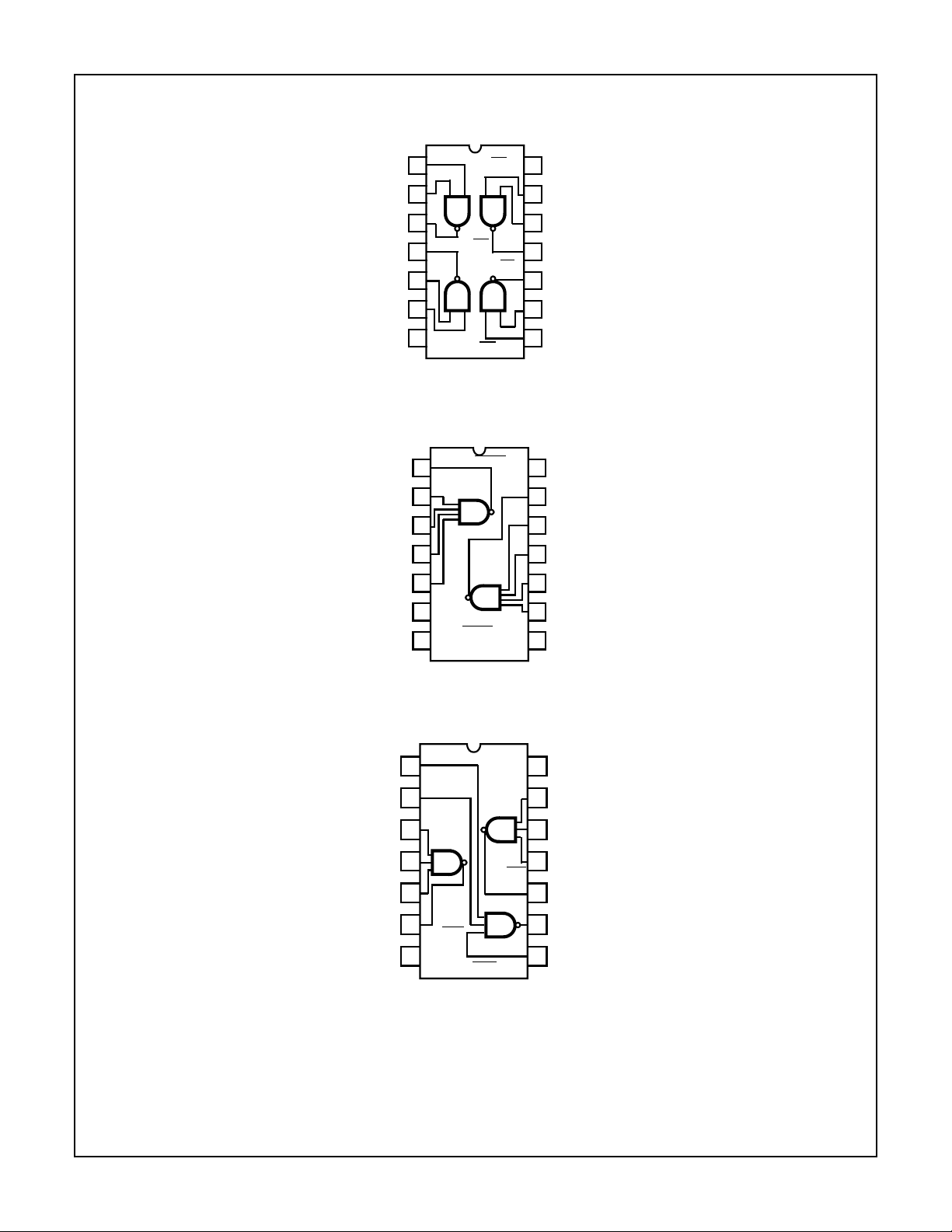
CD4011BMS - Quad 2 Input
CD4012BMS - Dual 4 Input
CD4023BMS - Triple 3 Input
CD4011BMS, CD4012BMS, and CD4023BMS NAND gates
provide the system designer with direct implementation of
the NAND function and supplement the existing family of
CMOS gates. All inputs and outputs are buffered.
Pinouts
AB
J =
K = CD
VSS
J = ABCD
NC
VSS
A
1
2
B
3
4
C
5
D
6
7
1
2
A
3
B
4
C
5
D
6
7
CMOS NAND Gates
CD4011BMS
TOP VIEW
VDD
14
H
13
G
12
M = GH
11
EF
10
L =
E
9
F
8
CD4012BMS
TOP VIEW
14
VDD
EFGH
13
K =
12
H
11
G
10
F
E
9
8
NC
NC = NO CONNECTION
CD4023BMS
TOP VIEW
The CD4011BMS, CD4012BMS and the CD4023BMS is
supplied in these 14 lead outline packages:
CD4011B CD4012B CD4023B
Braze Seal DIP
Frit Seal DIP
Ceramic Flatpack
CAUTION: These devices are sensitive to electrostatic discharge; follow proper IC Handling Procedures.
1-888-INTERSIL or 321-724-7143 | Copyright © Intersil Corporation 1999
H4Q H4H H4Q
H1B H1B H1B
H3W H3W H3W
K =
7-53
DEF
VSS
A
1
B
2
3
D
4
E
5
F
6
7
VDD
14
G
13
12
H
11
I
GHI
10
L =
J =
ABC
9
8
C
File Number 3079

Functional Diagrams
CD4011BMS, CD4012BMS, CD4023BMS
VSS
VSS
NC
A
B
J
K
C
D
J
A
B
C
D
1
2
3
4
5
6
7
CD4011BMS
1
2
3
4
5
6
K = EFGH
7
J = AB
CD
K =
L =
M =
GH
J = ABCD
EF
VDD
14
13
H
12
G
11
M
10
L
9
E
8
F
14
VDD
13
K
12
H
11
G
10
F
9
E
8
NC
NC = NO CONNECTION
VSS
CD4012BMS
A
1
2
B
3
D
4
E
F
5
K
6
K = DEF
7
J =
ABC
L =
GHI
14
VDD
13
G
12
H
11
I
10
L
J
9
8
C
CD4023BMS
7-54

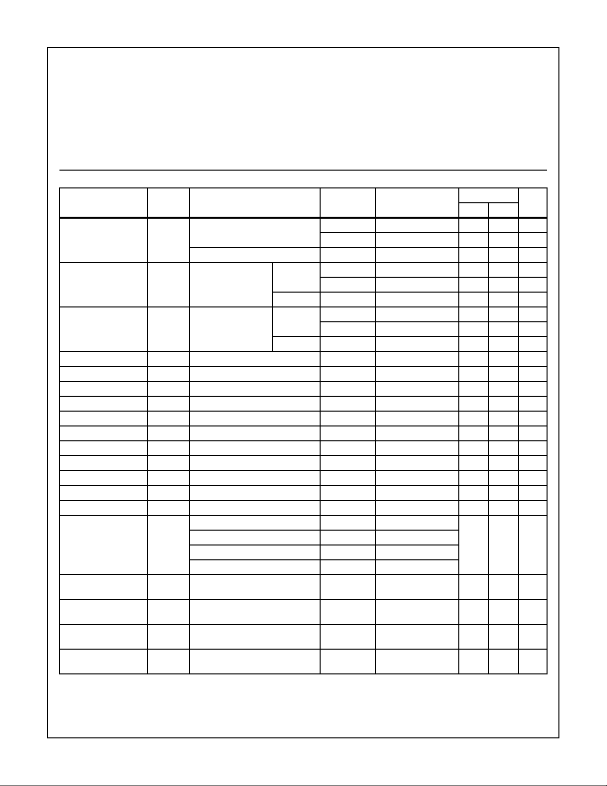
Specifications CD4011BMS, CD4012BMS, CD4023BMS
Absolute Maximum Ratings Reliability Information
DC Supply Voltage Range, (VDD) . . . . . . . . . . . . . . . -0.5V to +20V
(Voltage Referenced to VSS Terminals)
Input Voltage Range, All Inputs . . . . . . . . . . . . .-0.5V to VDD +0.5V
DC Input Current, Any One Input . . . . . . . . . . . . . . . . . . . . . . . .±10mA
Operating Temperature Range. . . . . . . . . . . . . . . . -55
Package Types D, F, K, H
Storage Temperature Range (TSTG). . . . . . . . . . . -65
o
C to +125oC
o
C to +150oC
Lead Temperature (During Soldering) . . . . . . . . . . . . . . . . . +265
At Distance 1/16 ± 1/32 Inch (1.59mm ± 0.79mm) from case for
10s Maximum
TABLE 1. DC ELECTRICAL PERFORMANCE CHARACTERISTICS
PARAMETER SYMBOL CONDITIONS (NOTE 1)
Supply Current IDD VDD = 20V, VIN = VDD or GND 1 +25
VDD = 18V, VIN = VDD or GND 3 -55oC - 0.5 µA
Input Leakage Current IIL VIN = VDD or GND VDD = 20 1 +25
VDD = 18V 3 -55oC -100 - nA
Input Leakage Current IIH VIN = VDD or GND VDD = 20 1 +25oC - 100 nA
VDD = 18V 3 -55oC - 100 nA
Output Voltage VOL15 VDD = 15V, No Load 1, 2, 3 +25oC, +125oC, -55oC - 50 mV
Output Voltage VOH15 VDD = 15V, No Load (Note 3) 1, 2, 3 +25oC, +125oC, -55oC 14.95 - V
Output Current (Sink) IOL5 VDD = 5V, VOUT = 0.4V 1 +25oC 0.53 - mA
Output Current (Sink) IOL10 VDD = 10V, VOUT = 0.5V 1 +25oC 1.4 - mA
Output Current (Sink) IOL15 VDD = 15V, VOUT = 1.5V 1 +25oC 3.5 - mA
Output Current (Source) IOH5A VDD = 5V, VOUT = 4.6V 1 +25oC - -0.53 mA
Output Current (Source) IOH5B VDD = 5V, VOUT = 2.5V 1 +25oC - -1.8 mA
Output Current (Source) IOH10 VDD = 10V, VOUT = 9.5V 1 +25oC - -1.4 mA
Output Current (Source) IOH15 VDD = 15V, VOUT = 13.5V 1 +25oC - -3.5 mA
N Threshold Voltage VNTH VDD = 10V, ISS = -10µA 1 +25oC -2.8 -0.7 V
P Threshold Voltage VPTH VSS = 0V, IDD = 10µA 1 +25oC 0.7 2.8 V
Functional F VDD = 2.8V, VIN = VDD or GND 7 +25oC VOH >
VDD = 20V, VIN = VDD or GND 7 +25oC
VDD = 18V, VIN = VDD or GND 8A +125oC
VDD = 3V, VIN = VDD or GND 8B -55oC
Input Voltage Low
VIL VDD = 5V, VOH > 4.5V, VOL < 0.5V 1, 2, 3 +25oC, +125oC, -55oC - 1.5 V
(Note 2)
Input Voltage High
VIH VDD = 5V, VOH > 4.5V, VOL < 0.5V 1, 2, 3 +25oC, +125oC, -55oC 3.5 - V
(Note 2)
Input Voltage Low
(Note 2)
Input Voltage High
(Note 2)
VIL VDD = 15V, VOH > 13.5V,
VOL < 1.5V
VIH VDD = 15V, VOH > 13.5V,
VOL < 1.5V
NOTES: 1. All voltages referenced to device GND, 100% testing being
implemented.
2. Go/No Go test with limits applied to inputs
Thermal Resistance . . . . . . . . . . . . . . . . θ
Ceramic DIP and FRIT Package. . . . . 80oC/W 20oC/W
Flatpack Package . . . . . . . . . . . . . . . . 70
Maximum Package Power Dissipation (PD) at +125oC
For TA = -55
For TA = +100
o
C
Device Dissipation per Output Transistor . . . . . . . . . . . . . . . 100mW
o
C to +100oC (Package Type D, F, K) . . . . . .500mW
o
C to +125oC (Package Type D, F, K) . . . . .Derate
Linearity at 12mW/oC to 200mW
ja
o
C/W 20oC/W
For TA = Full Package Temperature Range (All Package Types)
Junction Temperature . . . . . . . . . . . . . . . . . . . . . . . . . . . . . . +175oC
GROUP A
LIMITS
SUBGROUPS TEMPERATURE
o
C - 0.5 µA
2 +125oC-50µA
o
C -100 - nA
2 +125oC -1000 - nA
2 +125oC - 1000 nA
VOL <
VDD/2
VDD/2
1, 2, 3 +25oC, +125oC, -55oC- 4 V
1, 2, 3 +25oC, +125oC, -55oC11 - V
3. For accuracy, voltage is measured differentially to VDD. Limit
is 0.050V max.
θ
jc
UNITSMIN MAX
V
7-55
 Loading...