December 1992
CD40104BMS,
CD40194BMS
CMOS 4-Bit Bidirectional
Universal Shift Register
Features
• High Voltage Type (20V Rating)
• Medium Speed fCL = 12MHz (typ.) at VDD = 10V
• Fully Static Operation
• Synchronous Parallel or Serial Operation
• Three State Outputs (CD40104BMS)
• Asynchronous Master Reset (CD40194BMS)
• 5V, 10V and 15V Parametric Ratings
• Standardized Symmetrical Output Characteristics
• Meets All Requirements of JEDEC Tentative Standard
No. 13B, “Standard Specifications for Description of
‘B’ Series CMOS Devices”
Applications
• Arithmetic Unit Bus Registers
• Serial/Parallel Conversions
• General Purpose Register for Bus Organized Systems
• General Purpose Registers
Description
The CD40104BMS is a universal shift register featuring parallel
inputs, parallel outputs, SHIFT RIGHT and SHIFT LEFT serial
inputs, and a high impedance third output state allowing the device
to be used in bus organized systems.
In the parallel load mode (S0 and S1 are high), data is loaded into
the associated flip-flop and appears at the output after the positive
transition of the CLOCK input. During loading, serial data flow is
inhibited. Shift right and shift left are accomplished synchronously
on the positive clock edge with serial data entered at the SHIFT
RIGHT and SHIFT LEFT serial inputs, respectively. Clearing the
register is accomplished by setting both mode controls low and
clocking the register. When the output enable input is low, all outputs
assume the high impedance state.
The CD40194BMS is a universal shift register featuring parallel inputs,
parallel outputs SHIFT RIGHT and SHIFT LEFT serial inputs, and a
direct overriding clear input. In the parallel load mode (S0 and S1 are
high), data is loaded into the associated flip-flop and appears at the output after the positive transition of the CLOCK input. During loading,
serial data flow is inhibited. Shift right and shift left are accomplished
synchronously on the positive clock edge with data entered at the
SHIFT RIGHT and SHIFT LEFT serial inputs, respectively. Clocking of
the register is inhibited when both mode control inputs are low. When
low, the RESET input resets all stages and forces all outputs low. The
CD40194BMS is similar to industry types 340194 and MC40194.
The CD40104BMS and CD40194BMS series types are supplied in
these 16 lead outline packages
Braze Seal DIP *HNX, †H4W
Frit Seal DIP *H1L, †HIF
Ceramic Flatpack H6W
* CD40104B Only †CD40194B Only
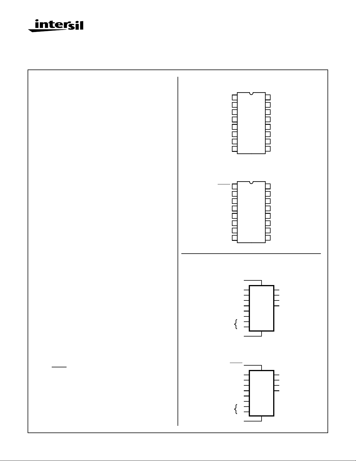
Pinouts
CD40104BMS
TOP VIEW
D0
D1
D2
D3
VSS
1
2
3
4
5
6
7
8
OUTPUT ENABLE
SHIFT RIGHT IN
SHIFT LEVEL IN
CD40194BMS
TOP VIEW
1
RESET
D0
D1
D2
D3
VSS
2
3
4
5
6
7
8
SHIFT RIGHT IN
SHIFT LEVEL IN
Functional Diagrams
CD40104BMS
OUTPUT ENABLE
3
D0
4
D1
5
D2
6
D3
SHIFT LEFT IN
SHIFT RIGHT IN
MODE SELECT
SHIFT LEFT IN
SHIFT RIGHT IN
MODE SELECT
7
2
9
S0
10
S1
CLOCK
CD40194BMS
RESET
3
D0
4
D1
5
D2
6
D3
7
2
9
S0
10
S1
CLOCK
16
VDD
15
Q0
14
Q1
13
Q2
12
Q3
11
CLOCK
10
SELECT 1
9
SELECT 0
16
VDD
15
Q0
14
Q1
13
Q2
12
Q3
11
CLOCK
10
SELECT 1
9
SELECT 0
1
15
Q0
14
Q1
13
Q2
12
Q3
15
14
13
12
VDD = 16
VSS = 8
Q0
Q1
Q2
Q3
VDD = 16
VSS = 8
11
1
11
CAUTION: These devices are sensitive to electrostatic discharge; follow proper IC Handling Procedures.
1-888-INTERSIL or 321-724-7143 | Copyright © Intersil Corporation 1999
7-1307
File Number 3352

Specifications CD40104BMS, CD40194BMS
Absolute Maximum Ratings Reliability Information
DC Supply Voltage Range, (VDD) . . . . . . . . . . . . . . . -0.5V to +20V
(Voltage Referenced to VSS Terminals)
Input Voltage Range, All Inputs . . . . . . . . . . . . .-0.5V to VDD +0.5V
DC Input Current, Any One Input . . . . . . . . . . . . . . . . . . . . . . . .±10mA
Operating Temperature Range. . . . . . . . . . . . . . . . -55oC to +125oC
Package Types D, F, K, H
Storage Temperature Range (TSTG) . . . . . . . . . . . -65oC to +150oC
Lead Temperature (During Soldering) . . . . . . . . . . . . . . . . . +265oC
At Distance 1/16 ± 1/32 Inch (1.59mm ± 0.79mm) from case for
10s Maximum
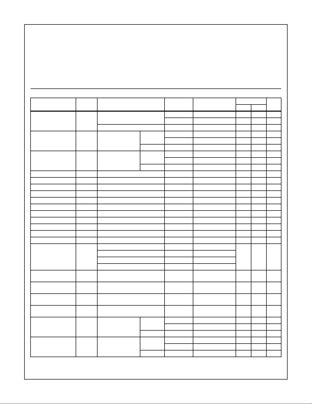
TABLE 1. DC ELECTRICAL PERFORMANCE CHARACTERISTICS
PARAMETER SYMBOL CONDITIONS (NOTE 1)
Supply Current IDD VDD = 20V, VIN = VDD or GND 1 +25oC-10µA
VDD = 18V, VIN = VDD or GND 3 -55oC-10µA
Input Leakage Current IIL VIN = VDD or GND VDD = 20V 1 +25oC -100 - nA
VDD = 18V 3 -55oC -100 - nA
Input Leakage Current IIH VIN = VDD or GND VDD = 20V 1 +25oC - 100 nA
VDD = 18V 3 -55oC - 100 nA
Output Voltage VOL15 VDD = 15V, No Load 1, 2, 3 +25oC, +125oC, -55oC - 50 mV
Output Voltage VOH15 VDD = 15V, No Load (Note 3) 1, 2, 3 +25oC, +125oC, -55oC 14.95 - V
Output Current (Sink) IOL5 VDD = 5V, VOUT = 0.4V 1 +25oC 0.53 - mA
Output Current (Sink) IOL10 VDD = 10V, VOUT = 0.5V 1 +25oC 1.4 - mA
Output Current (Sink) IOL15 VDD = 15V, VOUT = 1.5V 1 +25oC 3.5 - mA
Output Current (Source) IOH5A VDD = 5V, VOUT = 4.6V 1 +25oC - -0.53 mA
Output Current (Source) IOH5B VDD = 5V, VOUT = 2.5V 1 +25oC - -1.8 mA
Output Current (Source) IOH10 VDD = 10V, VOUT = 9.5V 1 +25oC - -1.4 mA
Output Current (Source) IOH15 VDD = 15V, VOUT = 13.5V 1 +25oC - -3.5 mA
N Threshold Voltage VNTH VDD = 10V, ISS = -10µA 1 +25oC -2.8 -0.7 V
P Threshold Voltage VPTH VSS = 0V, IDD = 10µA 1 +25oC 0.7 2.8 V
Functional F VDD = 2.8V, VIN = VDD or GND 7 +25oC VOH >
VDD = 20V, VIN = VDD or GND 7 +25oC
VDD = 18V, VIN = VDD or GND 8A +125oC
VDD = 3V, VIN = VDD or GND 8B -55oC
Input Voltage Low
(Note 2)
Input Voltage High
(Note 2)
Input Voltage Low
(Note 2)
Input Voltage High
(Note 2)
Tri-State Output
Leakage
Tri-State Output
Leakage
NOTES: 1. All voltages referenced to device GND, 100% testing being
implemented.
2. Go/No Go test with limits applied to inputs.
VIL VDD = 5V, VOH > 4.5V, VOL < 0.5V 1, 2, 3 +25oC, +125oC, -55oC - 1.5 V
VIH VDD = 5V, VOH > 4.5V, VOL < 0.5V 1, 2, 3 +25oC, +125oC, -55oC 3.5 - V
VIL VDD = 15V, VOH > 13.5V,
VOL < 1.5V
VIH VDD = 15V, VOH > 13.5V,
VOL < 1.5V
IOZL VIN = VDD or GND
VOUT = 0V
IOZH VIN = VDD or GND
VOUT = VDD
VDD = 20V 1 +25oC -0.4 - µA
VDD = 18V 3 -55oC -0.4 - µA
VDD = 20V 1 +25oC - 0.4 µA
VDD = 18V 3 -55oC - 0.4 µA
Thermal Resistance . . . . . . . . . . . . . . . . θ
Ceramic DIP and FRIT Package. . . . . 80oC/W 20oC/W
Flatpack Package . . . . . . . . . . . . . . . . 70oC/W 20oC/W
Maximum Package Power Dissipation (PD) at +125oC
For TA = -55oC to +100oC (Package Type D, F, K) . . . . . . 500mW
For TA = +100oC to +125oC (Package Type D, F, K). . . . . .Derate
Linearity at 12mW/oC to 200mW
Device Dissipation per Output Transistor . . . . . . . . . . . . . . . 100mW
For TA = Full Package Temperature Range (All Package Types)
Junction Temperature . . . . . . . . . . . . . . . . . . . . . . . . . . . . . . +175oC
GROUP A
SUBGROUPS TEMPERATURE
2 +125oC - 1000 µA
2 +125oC -1000 - nA
2 +125oC - 1000 nA
1, 2, 3 +25oC, +125oC, -55oC- 4 V
1, 2, 3 +25oC, +125oC, -55oC11 - V
2 +125oC -12 - µA
2 +125oC-12µA
3. For accuracy, voltage is measured differentially to VDD. Limit
is 0.050V max.
ja
LIMITS
VDD/2
VOL <
VDD/2
θ
jc
UNITSMIN MAX
V
7-1308

Specifications CD40104BMS, CD40194BMS
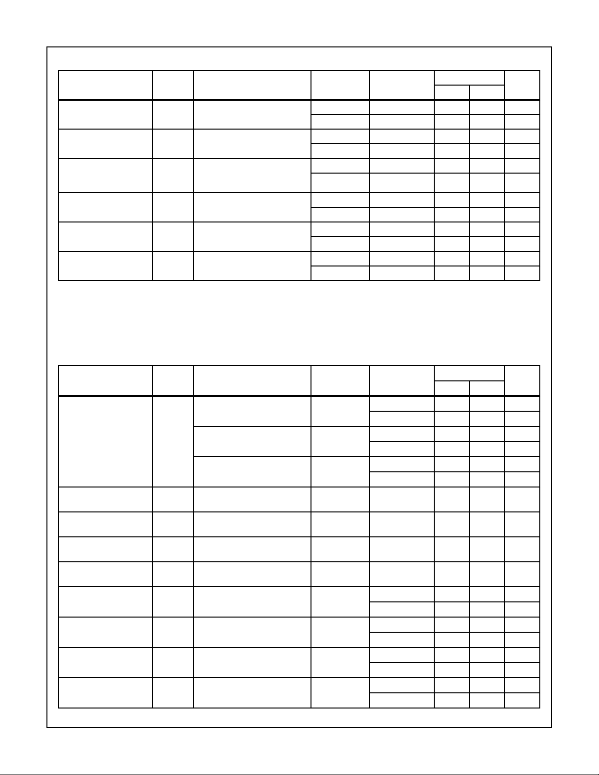
TABLE 2. AC ELECTRICAL PERFORMANCE CHARACTERISTICS
PARAMETER SYMBOL CONDITIONS
Propagation Delay
Clock to Q
Propagation Delay
CD40194BMS Reset to Q
Propagation Delay
CD40104BMS 3-State
Propagation Delay
CD40104BMS 3-State
Transition Time TTHL
Maximum Clock Input
Frequency
NOTES:
1. CL = 50pF, RL = 200K, Input TR, TF < 20ns.
2. -55oC and +125oC limits guaranteed, 100% testing being implemented.
3. VDD = 5V, CL = 50pF, RL = 1K, Input TR, TF < 20ns.
TPHL
TPLH
TPHL VDD = 5V, VIN = VDD or GND
TPZH
TPZL
TPLZ
TPHZ VDD = 5V, VIN = VDD or GND
TTLH
FCL VDD = 5V, VIN = VDD or GND
VDD = 5V, VIN = VDD or GND
(Note 1, 2)
(Note 1, 2)
VDD = 5V, VIN = VDD or GND
(Note 2, 3)
(Note 2, 3)
VDD = 5V, VIN = VDD or GND
(Note 1, 2)
(Note 1, 2)
GROUP A
SUBGROUPS TEMPERATURE
9 +25oC - 440 ns
10, 11 +125oC, -55oC - 594 ns
9 +25oC - 460 ns
10, 11 +125oC, -55oC - 621 ns
9 +25oC - 160 ns
10, 11 +125oC, -55oC - 216 ns
9 +25oC - 90 ns
10, 11 +125oC, -55oC - 122 ns
9 +25oC - 200 ns
10, 11 +125oC, -55oC - 270 ns
9 +25oC 3 - MHz
10, 11 +125oC, -55oC 2.22 - MHz
LIMITS
UNITSMIN MAX
TABLE 3. ELECTRICAL PERFORMANCE CHARACTERISTICS
LIMITS
PARAMETER SYMBOL CONDITIONS NOTES TEMPERATURE
o
Supply Current IDD VDD = 5V, VIN = VDD or GND 1, 2 -55
VDD = 10V, VIN = VDD or GND 1, 2 -55oC, +25oC- 10µA
VDD = 15V, VIN = VDD or GND 1, 2 -55oC, +25oC- 10µA
Output Voltage VOL VDD = 5V, No Load 1, 2 +25oC, +125oC,
Output Voltage VOL VDD = 10V, No Load 1, 2 +25oC, +125oC,
Output Voltage VOH VDD = 5V, No Load 1, 2 +25oC, +125oC,
Output Voltage VOH VDD = 10V, No Load 1, 2 +25oC, +125oC,
Output Current (Sink) IOL5 VDD = 5V, VOUT = 0.4V 1, 2 +125oC 0.36 - mA
Output Current (Sink) IOL10 VDD = 10V, VOUT = 0.5V 1, 2 +125oC 0.9 - mA
Output Current (Sink) IOL15 VDD = 15V, VOUT = 1.5V 1, 2 +125oC 2.4 - mA
Output Current (Source) IOH5A VDD = 5V, VOUT = 4.6V 1, 2 +125oC - -0.36 mA
C, +25oC- 5 µA
+125oC - 150 µA
+125oC - 300 µA
+125oC - 600 µA
-50mV
-55oC
-50mV
-55oC
4.95 - V
-55oC
9.95 - V
-55oC
-55oC 0.64 - mA
-55oC 1.6 - mA
-55oC 4.2 - mA
-55oC - -0.64 mA
UNITSMIN MAX
7-1309
 Loading...