Intersil Corporation CD40181BMS Datasheet

CD40181BMS
December 1992
Features
• High Voltage Type (20V Rating)
• Full Look Ahead Carry for Speed Operations on Long
Words
• Generates 16 Logic Functions of Two Boolean Variables
• Generates 16 Arithmetic Functions of T wo 4 Bit Binary
Words
• A = B comparator Output Available
• Ripple Carry Input and Output Available
• Typical Addition Time 200ns at VDD = 10V
• 100% Tested for Quiescent Current at 20V
• 5V, 10V and 15V Parametric Ratings
• Maximum Input Current of 1µA at 18V Over Full Package Temperature Range; 100nA at 18V and +25
• Noise Margin (Over Full Package/Temperature Range)
- 1V at VDD = 5V
- 2V at VDD = 10V
- 2.5V at VDD = 15V
• Standardized Symmetrical Output Characteristics
• Meets All Requirements of JEDEC Tentative Standard
No. 13B, “Standard Specifications for Description of
‘B’ Series CMOS Devices”
Applications
• Parallel Arithmetic Units
• Process Controllers
• Low Power Minicomputers
CMOS 4 Bit Arithmetic Logic Unit
Description
The CD40181BMS is a low power four bit parallel arithmetic
logic unit (ALU) capable of providing 16 binary arithmetic
operations on two four-bit words and 16 logical functions of
two Boolean variables. The mode control input M selects
logical (M = High) or arithmetic (M = Low) operation. The
four select inputs (S0, S1, S2, and S3) select the desired
logical or arithmetic functions, which include AND, OR,
NAND, NOR and exclusive-OR and-NOR in the logic mode,
and addition, subtraction, decrement, left-shift and straight
transfer in the arithmetic mode, according to the truth table.
The CD40181BMS operation may be interpreted with either
active-low or active-high data at the A and B word inputs and
o
C
the function outputs F, by using the appropriate truth table.
The CD40181BMS contains logic for full look ahead carry
operation for fast carry generation using the carry-generate
and carry-propagate outputs
G and P for the four bits of the
CD40181BMS. Use of the CD40182BMS look-ahead carry
generator in conjunction with multiple CD40181BMS’s
permits high speed arithmetic operations on long words. A
ripple carry output Cn+4 is available for use in systems
where speed is not of primary importance.
Also included in the CD40181BMS is a comparator output
A = B, which assumes a high level whenever the two four-bit
input words A and B are equal and the device is in the
subtract mode. In addition, relative magnitude information
may be derived from the carry-in input Cn and ripple carryout output Cn+4 by placing the unit in the subtract mode and
externally decoding using the information in Table B.
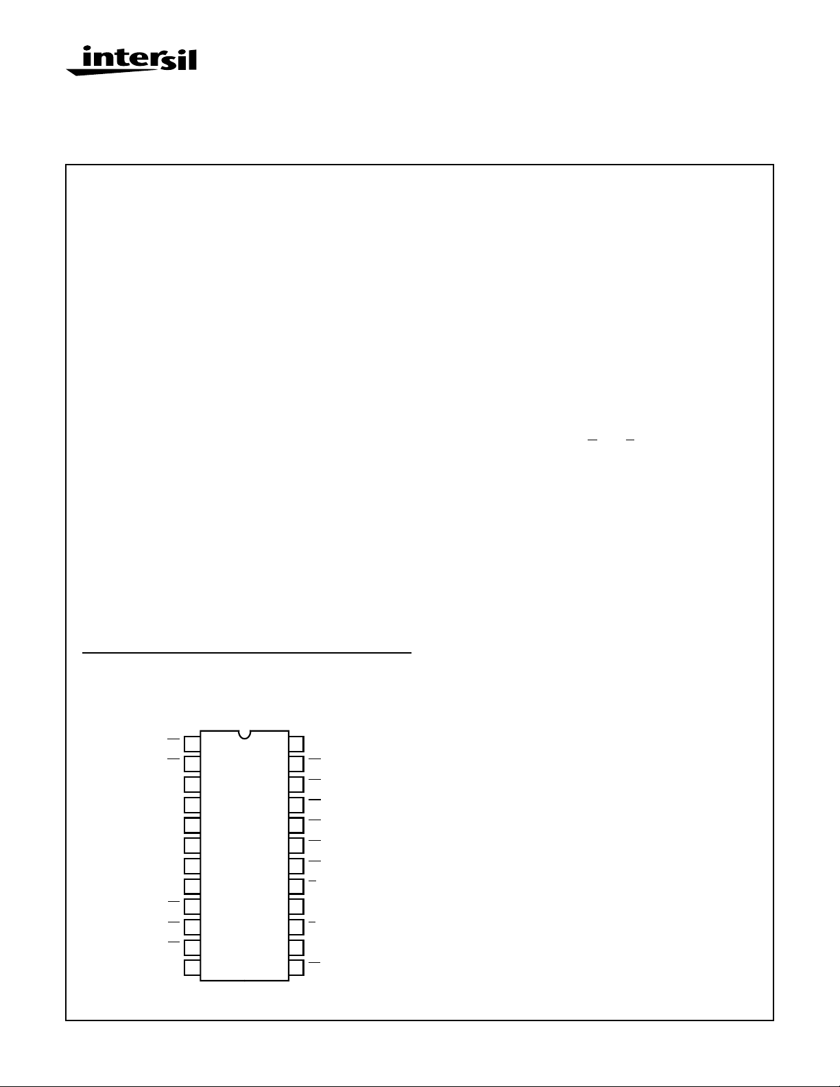
Pinout
CD40181BMS ACTIVE-LOW DATA
TOP VIEW
1
B0
2
A0
3
S3
4
S2
5
S1
6
S0
7
Cn
8
M
9
F0
10
F1
11
F2
12
VSS
CAUTION: These devices are sensitive to electrostatic discharge; follow proper IC Handling Procedures.
1-888-INTERSIL or 321-724-7143 | Copyright © Intersil Corporation 1999
24
VDD
23
A1
22
B1
21
A2
20
B2
19
A3
18
B3
17
G
16
Cn+4
15
P
14
A = B
13
F3
The CD40181BMS is similar to industry types MC14581 and
74181.
The CD40181BMS is supplied in these 24-lead outline
packages:
Braze Seal DIP HNZ
Ceramic Flatpack H4P
7-1400
File Number
3361

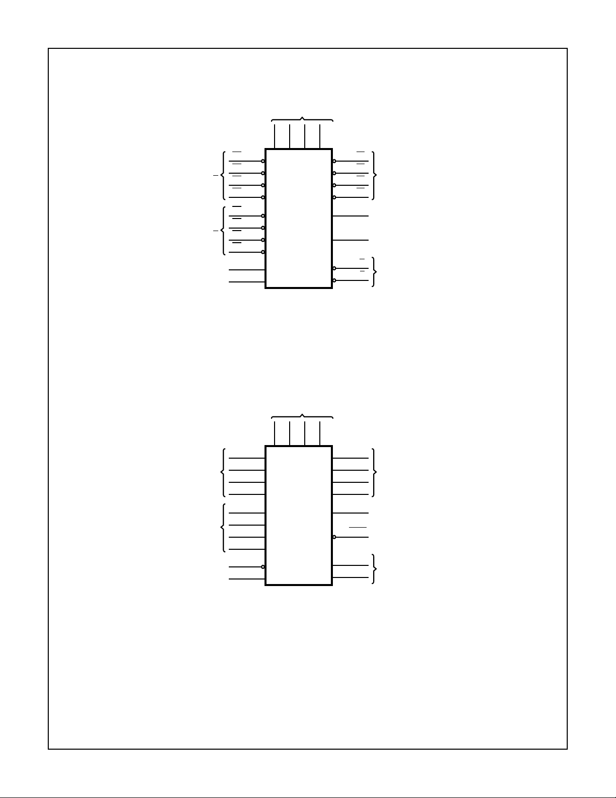
Functional Diagrams
WORD
CD40181BMS
FUNCTION SELECT
INPUTS
S3
6S05S14S23
A0 2
A1 23
A
A2 21
A3 19
F09
F110
F211
F313
OUTPUT
FUNCTION
WORD
B
CARRY IN
MODE
CONTROL
WORD
A
B0 1
B1 22
B2 20
B3 18
Cn 7
M8
VDD = 24
VSS = 12
A0 2
A1 23
A2 21
A3 19
14 A = B
16 Cn+4
ACTIVE-LOW DATA
FUNCTION SELECT
INPUTS
S3
6S05S14S23
COMPARE
OUT
RIPPLE
CARRY OUT
G17
P15
F09
F110
F211
F313
LOOK AHEAD
CARRY
OUTPUTS
OUTPUT
FUNCTION
WORD
B
CARRY IN
MODE
CONTROL
B0 1
B1 22
B2 20
B3 18
Cn 7
M8
VDD = 24
VSS = 12
14 A = B
16
ACTIVE-HIGH DATA
7-1401
Cn+4
G17
COMPARE
OUT
RIPPLE
CARRY OUT
LOOK AHEAD
CARRY
P15
OUTPUTS

Specifications CD40181BMS
Absolute Maximum Ratings Reliability Information
DC Supply Voltage Range, (VDD) . . . . . . . . . . . . . . . -0.5V to +20V
(Voltage Referenced to VSS Terminals)
Input Voltage Range, All Inputs . . . . . . . . . . . . .-0.5V to VDD +0.5V
DC Input Current, Any One Input . . . . . . . . . . . . . . . . . . . . . . . .±10mA
Operating Temperature Range. . . . . . . . . . . . . . . . -55oC to +125oC
Package Types D, F, K, H
Storage Temperature Range (TSTG). . . . . . . . . . . -65oC to +150oC
Lead Temperature (During Soldering) . . . . . . . . . . . . . . . . . +265oC
At Distance 1/16 ± 1/32 Inch (1.59mm ± 0.79mm) from case for
10s Maximum
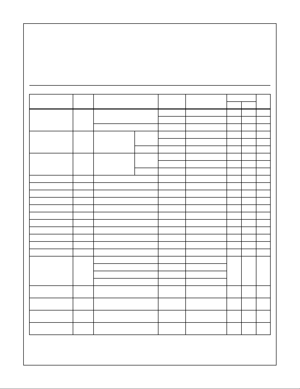
TABLE 1. DC ELECTRICAL PERFORMANCE CHARACTERISTICS
PARAMETER SYMBOL CONDITIONS (NOTE 1)
Supply Current IDD VDD = 20V, VIN = VDD or GND 1 +25oC-10µA
VDD = 18V, VIN = VDD or GND 3 -55oC-10µA
Input Leakage Current IIL VIN = VDD or GND VDD = 20 1 +25oC -100 - nA
VDD = 18V 3 -55oC -100 - nA
Input Leakage Current IIH VIN = VDD or GND VDD = 20 1 +25oC - 100 nA
VDD = 18V 3 -55oC - 100 nA
Output Voltage VOL15 VDD = 15V, No Load 1, 2, 3 +25oC, +125oC, -55oC - 50 mV
Output Voltage VOH15 VDD = 15V, No Load (Note 3) 1, 2, 3 +25oC, +125oC, -55oC 14.95 - V
Output Current (Sink) IOL5 VDD = 5V, VOUT = 0.4V 1 +25oC 0.53 - mA
Output Current (Sink) IOL10 VDD = 10V, VOUT = 0.5V 1 +25oC 1.4 - mA
Output Current (Sink) IOL15 VDD = 15V, VOUT = 1.5V 1 +25oC 3.5 - mA
Output Current (Source) IOH5A VDD = 5V, VOUT = 4.6V 1 +25oC - -0.53 mA
Output Current (Source) IOH5B VDD = 5V, VOUT = 2.5V 1 +25oC - -1.8 mA
Output Current (Source) IOH10 VDD = 10V, VOUT = 9.5V 1 +25oC - -1.4 mA
Output Current (Source) IOH15 VDD = 15V, VOUT = 13.5V 1 +25oC - -3.5 mA
N Threshold Voltage VNTH VDD = 10V, ISS = -10µA 1 +25oC -2.8 -0.7 V
P Threshold Voltage VPTH VSS = 0V, IDD = 10µA 1 +25oC 0.7 2.8 V
Functional F VDD = 2.8V, VIN = VDD or GND 7 +25oC VOH >
VDD = 20V, VIN = VDD or GND 7 +25oC
VDD = 18V, VIN = VDD or GND 8A +125oC
VDD = 3V, VIN = VDD or GND 8B -55oC
Input Voltage Low
(Note 2)
Input Voltage High
(Note 2)
Input Voltage Low
(Note 2)
Input Voltage High
(Note 2)
NOTES: 1. All voltages referenced to device GND, 100% testing being
implemented.
2. Go/No Go test with limits applied to inputs.
VIL VDD = 5V, VOH > 4.5V, VOL < 0.5V 1, 2, 3 +25oC, +125oC, -55oC - 1.5 V
VIH VDD = 5V, VOH > 4.5V, VOL < 0.5V 1, 2, 3 +25oC, +125oC, -55oC 3.5 - V
VIL VDD = 15V, VOH > 13.5V,
VOL < 1.5V
VIH VDD = 15V, VOH > 13.5V,
VOL < 1.5V
Thermal Resistance θ
Ceramic DIP and FRIT Package. . . . . 80oC/W 20oC/W
Flatpack Package . . . . . . . . . . . . . . . . 70oC/W 20oC/W
Maximum Package Power Dissipation (PD) at +125oC
For TA = -55oC to +100oC (Package Type D, F, K) . . . . . .500mW
For TA = +100oC to +125oC (Package Type D, F, K). . . . . .Derate
Linearity at 12mW/oC to 200mW
Device Dissipation per Output Transistor . . . . . . . . . . . . . . . 100mW
For TA = Full Package Temperature Range (All Package Types)
Junction Temperature . . . . . . . . . . . . . . . . . . . . . . . . . . . . . . +175oC
GROUP A
SUBGROUPS TEMPERATURE
2 +125oC - 1000 µA
2 +125oC -1000 - nA
2 +125oC - 1000 nA
1, 2, 3 +25oC, +125oC, -55oC- 4 V
1, 2, 3 +25oC, +125oC, -55oC11 - V
3. For accuracy, voltage is measured differentially to VDD. Limit
is 0.050V max.
ja
LIMITS
VDD/2
VOL <
VDD/2
θ
jc
UNITSMIN MAX
V
7-1402
 Loading...