

CD40175BMS
December 1992
Features
• High Voltage Type (20V Rating)
• Output Compatible with Two HTL Loads, Two Low Power
TTL Loads, or One Low Power Schottky TTL Load
• Functional Equivalent to TTL74175
• 100% Tested for Quiescent Current at 20V
• 5V, 10V and 15V Parametric Ratings
• Maximum Input Current of 1µA at 18V Over Full Package Temperature Range; 100nA at 18V and +25
• Noise Margin (Over Full Package/Temperature Range)
- 1V at VDD = 5V
- 2V at VDD = 10V
- 2.5V at VDD = 15V
• Standardized Symmetrical Output Characteristics
• Meets All Requirements of JEDEC Tentative Standard
No. 13B, “Standard Specifications for Description of
‘B’ Series CMOS Devices”
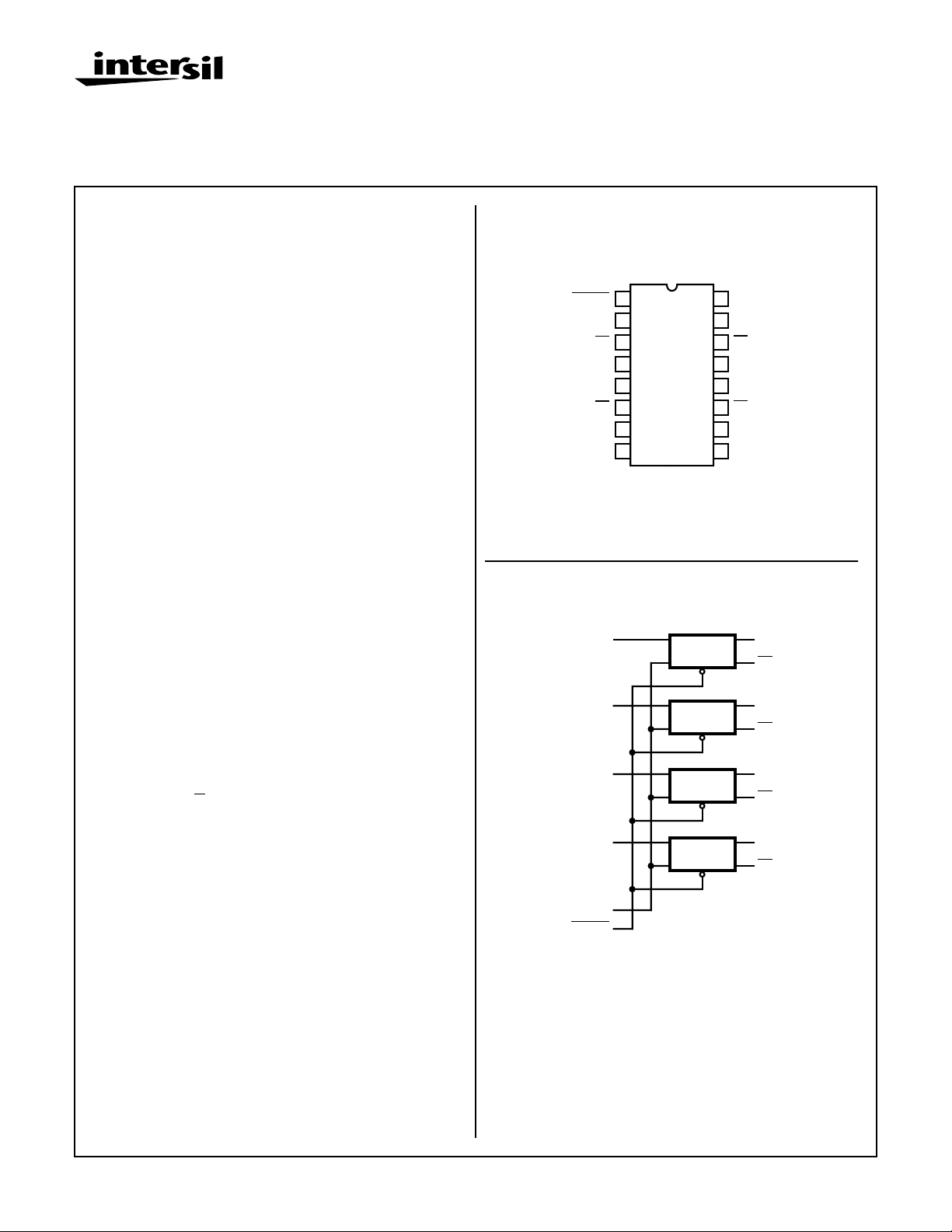
CMOS Quad ‘D’ Type Flip-Flop
Pinout
CD40175BMS
TOP VIEW
VDD
16
15
14
13
12
11
10
9
Q4
Q4
D4
D3
Q3
Q3
CLOCK
Q1
Q1
D1
D2
Q2
Q2
VSS
1
2
3
4
5
6
7
8
CLEAR
o
C
VDD = PIN 16
VSS = PIN 8
Functional Diagram
Applications
• Shift Registers
• Buffer/Storage Registers
• Pattern Generators
Description
CD40175BMS consists of four identical D-type flip-flops.
Each flip-flop has an independent DATA D input and complementary Q and
are common to all flip-flops. Data are transferred to the Q
outputs on the positive going transition of the clock pulse. All
four flip-flops are simultaneously reset by a low level on the
CLEAR input.
These devices can function as shift register elements or as
T-type flip-flops for toggle and counter applications.
The CD40175BMS is supplied in these 16-lead outline
packages:
Braze Seal DIP H4T
Ceramic Flatpack H6W
Q outputs. The CLOCK and CLEAR inputs
D1
D2
D3
D4
CLOCK
CLEAR
4
F/F1
5
F/F2
12
F/F3
13
F/F4
9
1
2
Q1
3
Q1
7
Q2
6
Q2
10
Q3
11
Q3
15
Q4
14
Q4
VSS = 8
VDD = 16
CAUTION: These devices are sensitive to electrostatic discharge; follow proper IC Handling Procedures.
1-888-INTERSIL or 321-724-7143 | Copyright © Intersil Corporation 1999
7-1392
File Number
3360
Specifications CD40175BMS
Absolute Maximum Ratings Reliability Information
DC Supply Voltage Range, (VDD) . . . . . . . . . . . . . . . -0.5V to +20V
(Voltage Referenced to VSS Terminals)
Input Voltage Range, All Inputs . . . . . . . . . . . . .-0.5V to VDD +0.5V
DC Input Current, Any One Input . . . . . . . . . . . . . . . . . . . . . . . .±10mA
Operating Temperature Range. . . . . . . . . . . . . . . . -55oC to +125oC
Package Types D, F, K, H
Storage Temperature Range (TSTG). . . . . . . . . . . -65oC to +150oC
Lead Temperature (During Soldering) . . . . . . . . . . . . . . . . . +265oC
At Distance 1/16 ± 1/32 Inch (1.59mm ± 0.79mm) from case for
10s Maximum
TABLE 1. DC ELECTRICAL PERFORMANCE CHARACTERISTICS
PARAMETER SYMBOL CONDITIONS (NOTE 1)
Supply Current IDD VDD = 20V, VIN = VDD or GND 1 +25oC-2µA
VDD = 18V, VIN = VDD or GND 3 -55oC-2µA
Input Leakage Current IIL VIN = VDD or GND VDD = 20 1 +25oC -100 - nA
VDD = 18V 3 -55oC -100 - nA
Input Leakage Current IIH VIN = VDD or GND VDD = 20 1 +25oC - 100 nA
VDD = 18V 3 -55oC - 100 nA
Output Voltage VOL15 VDD = 15V, No Load 1, 2, 3 +25oC, +125oC, -55oC - 50 mV
Output Voltage VOH15 VDD = 15V, No Load (Note 3) 1, 2, 3 +25oC, +125oC, -55oC 14.95 - V
Output Current (Sink) IOL5 VDD = 5V, VOUT = 0.4V 1 +25oC 0.53 - mA
Output Current (Sink) IOL10 VDD = 10V, VOUT = 0.5V 1 +25oC 1.4 - mA
Output Current (Sink) IOL15 VDD = 15V, VOUT = 1.5V 1 +25oC 3.5 - mA
Output Current (Source) IOH5A VDD = 5V, VOUT = 4.6V 1 +25oC - -0.53 mA
Output Current (Source) IOH5B VDD = 5V, VOUT = 2.5V 1 +25oC - -1.8 mA
Output Current (Source) IOH10 VDD = 10V, VOUT = 9.5V 1 +25oC - -1.4 mA
Output Current (Source) IOH15 VDD = 15V, VOUT = 13.5V 1 +25oC - -3.5 mA
N Threshold Voltage VNTH VDD = 10V, ISS = -10µA 1 +25oC -2.8 -0.7 V
P Threshold Voltage VPTH VSS = 0V, IDD = 10µA 1 +25oC 0.7 2.8 V
Functional F VDD = 2.8V, VIN = VDD or GND 7 +25oC VOH >
VDD = 20V, VIN = VDD or GND 7 +25oC
VDD = 18V, VIN = VDD or GND 8A +125oC
VDD = 3V, VIN = VDD or GND 8B -55oC
Input Voltage Low
(Note 2)
Input Voltage High
(Note 2)
Input Voltage Low
(Note 2)
Input Voltage High
(Note 2)
NOTES: 1. All voltages referenced to device GND, 100% testing being
implemented.
2. Go/No Go test with limits applied to inputs.
VIL VDD = 5V, VOH > 4.5V, VOL < 0.5V 1, 2, 3 +25oC, +125oC, -55oC - 1.5 V
VIH VDD = 5V, VOH > 4.5V, VOL < 0.5V 1, 2, 3 +25oC, +125oC, -55oC 3.5 - V
VIL VDD = 15V, VOH > 13.5V,
VOL < 1.5V
VIH VDD = 15V, VOH > 13.5V,
VOL < 1.5V
Thermal Resistance θ
Ceramic DIP and FRIT Package. . . . . 80oC/W 20oC/W
Flatpack Package . . . . . . . . . . . . . . . . 70oC/W 20oC/W
Maximum Package Power Dissipation (PD) at +125oC
For TA = -55oC to +100oC (Package Type D, F, K) . . . . . .500mW
For TA = +100oC to +125oC (Package Type D, F, K). . . . . .Derate
Linearity at 12mW/oC to 200mW
Device Dissipation per Output Transistor . . . . . . . . . . . . . . . 100mW
For TA = Full Package Temperature Range (All Package Types)
Junction Temperature . . . . . . . . . . . . . . . . . . . . . . . . . . . . . . +175oC
GROUP A
SUBGROUPS TEMPERATURE
2 +125oC - 200 µA
2 +125oC -1000 - nA
2 +125oC - 1000 nA
1, 2, 3 +25oC, +125oC, -55oC- 4 V
1, 2, 3 +25oC, +125oC, -55oC11 - V
3. For accuracy, voltage is measured differentially to VDD. Limit
is 0.050V max.
ja
LIMITS
VDD/2
VOL <
VDD/2
θ
jc
UNITSMIN MAX
V
7-1393
Specifications CD40175BMS
TABLE 2. AC ELECTRICAL PERFORMANCE CHARACTERISTICS
GROUP A
PARAMETER SYMBOL CONDITIONS (NOTES 1, 2)
Propagation Delay
Clock to Q Output
Propagation Delay
Clear to Q Output
Transition Time TTHL
Maximum Clock Input
Frequency
NOTES:
1. CL = 50pF, RL = 200K, Input TR, TF < 20ns
2. -55oC and +125oC limits guaranteed, 100% testing being implemented.
PARAMETER SYMBOL CONDITIONS NOTES TEMPERATURE
Supply Current IDD VDD = 5V, VIN = VDD or GND 1, 2 -55oC, +25oC- 1 µA
Output Voltage VOL VDD = 5V, No Load 1, 2 +25oC, +125oC,
Output Voltage VOL VDD = 10V, No Load 1, 2 +25oC, +125oC,
Output Voltage VOH VDD = 5V, No Load 1, 2 +25oC, +125oC,
Output Voltage VOH VDD = 10V, No Load 1, 2 +25oC, +125oC,
Output Current (Sink) IOL5 VDD = 5V, VOUT = 0.4V 1, 2 +125oC 0.36 - mA
Output Current (Sink) IOL10 VDD = 10V, VOUT = 0.5V 1, 2 +125oC 0.9 - mA
Output Current (Sink) IOL15 VDD = 15V, VOUT = 1.5V 1, 2 +125oC 2.4 - mA
Output Current (Source) IOH5A VDD = 5V, VOUT = 4.6V 1, 2 +125oC - -0.36 mA
Output Current (Source) IOH5B VDD = 5V, VOUT = 2.5V 1, 2 +125oC - -1.15 mA
Output Current (Source) IOH10 VDD = 10V, VOUT = 9.5V 1, 2 +125oC - -0.9 mA
TPHL1
TPLH1
TPHL2 VDD = 5V, VIN = VDD or GND 9 +25oC - 500 ns
TTLH
FCL VDD = 5V, VIN = VDD or GND 9 +25oC 2 - MHz
VDD = 5V, VIN = VDD or GND 9 +25oC - 400 ns
VDD = 5V, VIN = VDD or GND 9 +25oC - 200 ns
TABLE 3. ELECTRICAL PERFORMANCE CHARACTERISTICS
VDD = 10V, VIN = VDD or GND 1, 2 -55oC, +25oC- 2 µA
VDD = 15V, VIN = VDD or GND 1, 2 -55oC, +25oC- 2 µA
SUBGROUPS TEMPERATURE
10, 11 +125oC, -55oC - 540 ns
10, 11 +125oC, -55oC - 675 ns
10, 11 +125oC, -55oC - 270 ns
10, 11 +125oC, -55oC 1.48 - MHz
+125oC-30µA
+125oC-60µA
+125oC - 120 µA
-55oC
-55oC
-55oC
-55oC
-55oC 0.64 - mA
-55oC 1.6 - mA
-55oC 4.2 - mA
-55oC - -0.64 mA
-55oC - -2.0 mA
-55oC - -1.6 mA
LIMITS
UNITSMIN MAX
LIMITS
UNITSMIN MAX
-50mV
-50mV
4.95 - V
9.95 - V
7-1394

Specifications CD40175BMS
TABLE 3. ELECTRICAL PERFORMANCE CHARACTERISTICS (Continued)
LIMITS
PARAMETER SYMBOL CONDITIONS NOTES TEMPERATURE
Output Current (Source) IOH15 VDD =15V, VOUT = 13.5V 1, 2 +125oC - -2.4 mA
-55oC - -4.2 mA
Input Voltage Low VIL VDD = 10V, VOH > 9V , VOL < 1V 1, 2 +25oC, +125oC,
-55oC
Input Voltage High VIH VDD = 10V, VOH > 9V, VOL < 1V 1, 2 +25oC, +125oC,
-55oC
Propagation Delay
Clock to Q Output
Propagation Delay
Clear to Q Output
Transition Time TTHL
Minimum Data Setup
Time
Minimum Data Hold Time TH VDD = 5V 1, 2, 3 +25oC - 80 ns
Minimum Clear Pulse
Width
Maximum Clock Rise or
Fall Time
Minimum Clear Removal
Time (Clear to be High
before Positive Transition
of Clock)
Minimum Clock Pulse
Width
Input Capacitance CIN Any Input 1, 2 +25oC - 7.5 pF
NOTES:
1. All voltages referenced to device GND.
2. The parameters listed on Table 3 are controlled via design or process and are not directly tested. These parameters are characterized
on initial design release and upon design changes which would affect these characteristics.
3. CL = 50pF, RL = 200K, Input TR, TF < 20ns.
4. If more than one unit is cascaded, TRCL should be made less than or equal to the sumof the transition time and the fixed propagation
delay of the output of the driving stage for the estimated capacitive load.
TPHL1
TPLH1
TPHL2 VDD = 10V 1, 2, 3 +25oC - 200 ns
TTLH
TW VDD = 5V 1, 2, 3 +25oC - 200 ns
TRCL
TFCL
TREM VDD = 5V 1, 2, 3 +25oC - 250 ns
TW VDD = 5V 1, 2, 3 +25oC - 250 ns
VDD = 10V 1, 2, 3 +25oC - 160 ns
VDD = 15V 1, 2, 3 +25oC - 120 ns
VDD = 15V 1, 2, 3 +25oC - 150 ns
VDD = 10V 1, 2, 3 +25oC - 100 ns
VDD = 15V 1, 2, 3 +25oC - 80 ns
TS VDD = 5V 1, 2, 3 +25oC - 120 ns
VDD = 10V 1, 2, 3 +25oC - 50 ns
VDD = 15V 1, 2, 3 +25oC - 40 ns
VDD = 10V 1, 2, 3 +25oC - 40 ns
VDD = 15V 1, 2, 3 +25oC - 30 ns
VDD = 10V 1, 2, 3 +25oC - 80 ns
VDD = 15V 1, 2, 3 +25oC - 60 ns
VDD = 5V 1, 2, 3, 4 +25oC15-µs
VDD = 10V 1, 2, 3, 4 +25oC15-µs
VDD = 15V 1, 2, 3, 4 +25oC15-µs
VDD = 10V 1, 2, 3 +25oC - 100 ns
VDD = 15V 1, 2, 3 +25oC - 80 ns
VDD = 10V 1, 2, 3 +25oC - 100 ns
VDD = 15V 1, 2, 3 +25oC - 75 ns
-3V
7-V
UNITSMIN MAX
7-1395

Specifications CD40175BMS
TABLE 4. POST IRRADIATION ELECTRICAL PERFORMANCE CHARACTERISTICS
LIMITS
PARAMETER SYMBOL CONDITIONS NOTES TEMPERATURE
Supply Current IDD VDD = 20V, VIN = VDD or GND 1, 4 +25oC - 7.5 µA
N Threshold Voltage VNTH VDD = 10V, ISS = -10µA 1, 4 +25oC -2.8 -0.2 V
N Threshold Voltage
Delta
P Threshold Voltage VTP VSS = 0V, IDD = 10µA 1, 4 +25oC 0.2 2.8 V
P Threshold Voltage
Delta
Functional F VDD = 18V, VIN = VDD or GND 1 +25oC VOH >
Propagation Delay Time TPHL
NOTES: 1. All voltages referenced to device GND.
2. CL = 50pF, RL = 200K, Input TR, TF < 20ns.
∆VTN VDD = 10V, ISS = -10µA 1, 4 +25oC-±1V
∆VTP VSS = 0V, IDD = 10µA 1, 4 +25oC-±1V
VOL <
VDD = 3V, VIN = VDD or GND
VDD = 5V 1, 2, 3, 4 +25oC - 1.35 x
TPLH
3. See Table 2 for +25oC limit.
4. Read and Record
TABLE 5. BURN-IN AND LIFE TEST DELTA PARAMETERS +25oC
PARAMETER SYMBOL DELTA LIMIT
Supply Current - MSI-1 IDD ± 0.2µA
Output Current (Sink) IOL5 ± 20% x Pre-Test Reading
Output Current (Source) IOH5A ± 20% x Pre-Test Reading
VDD/2
VDD/2
+25oC
Limit
UNITSMIN MAX
ns
V
TABLE 6. APPLICABLE SUBGROUPS
MIL-STD-883
CONFORMANCE GROUP
Initial Test (Pre Burn-In) 100% 5004 1, 7, 9 IDD, IOL5, IOH5A
Interim Test 1 (Post Burn-In) 100% 5004 1, 7, 9 IDD, IOL5, IOH5A
Interim Test 2 (Post Burn-In) 100% 5004 1, 7, 9 IDD, IOL5, IOH5A
PDA (Note 1) 100% 5004 1, 7, 9, Deltas
Interim Test 3 (Post Burn-In) 100% 5004 1, 7, 9 IDD, IOL5, IOH5A, RONDEL10
PDA (Note 1) 100% 5004 1, 7, 9, Deltas
Final Test 100% 5004 2, 3, 8A, 8B, 10, 11
Group A Sample 5005 1, 2, 3, 7, 8A, 8B, 9, 10, 11
Group B Subgroup B-5 Sample 5005 1, 2, 3, 7, 8A, 8B, 9, 10, 11, Deltas Subgroups 1, 2, 3, 9, 10, 11
Subgroup B-6 Sample 5005 1, 7, 9
Group D Sample 5005 1, 2, 3, 8A, 8B, 9 Subgroups 1, 2 3
NOTE: 1. 5% Parameteric, 3% Functional; Cumulative for Static 1 and 2.
CONFORMANCE GROUPS
Group E Subgroup 2 5005 1, 7, 9 Table 4 1, 9 Table 4
METHOD GROUP A SUBGROUPS READ AND RECORD
TABLE 7. TOTAL DOSE IRRADIATION
MIL-STD-883
METHOD
PRE-IRRAD POST-IRRAD PRE-IRRAD POST-IRRAD
TEST READ AND RECORD
7-1396

Specifications CD40175BMS
TABLE 8. BURN-IN AND IRRADIATION TEST CONNECTIONS
OSCILLATOR
FUNCTION OPEN GROUND VDD 9V ± -0.5V
Static Burn-In 1
(Note 1)
Static Burn-In 2
(Note 1)
Dynamic BurnIn (Note 1)
Irradiation
(Note 2)
2, 3, 6, 7, 10, 11,
1, 4, 5, 8, 9, 12, 13 16
14, 15
2, 3, 6, 7, 10, 11,
14, 15
8 1, 4, 5, 9, 12,
13, 16
- 8 1, 16 2, 3, 6, 7, 10, 11,
2, 3, 6, 7, 10, 11,
14, 15
8 1, 4, 5, 9, 12,
13, 16
14, 15
50kHz 25kHz
9 4, 5, 12, 13
NOTES:
1. Each pin except VDD and GND will have a series resistor of 10K ± 5%, VDD = 18V ± 0.5V
2. Each pin except VDD and GND will have a series resistor of 47K ± 5%; Group E, Subgroup 2, sample size is 4 dice/wafer, 0 failures,
VDD = 10V ± 0.5V
Logic Diagram
CLR
CLK
CL
CL
CL
p
n
CL
p
n
CL
CL
*
D
*
1
*
9
CL
CL
p
n
CL
p
n
CL
Q
Q
ALL INPUTS ARE PROTECTED
*
BY CMOS PROTECTION
NETWORK
VDD
VSS
FIGURE 1. 1 OF 4 FLIP-FLOPS
TRUTH TABLE FOR 1 OF 4 FLIP-FLOPS (Positive Logic)
INPUTS OUTPUTS
CLOCK DATA CLEAR Q Q
0101
1110
X1QQ
XX001
1 = High level
X = Don’t care
0 = Low level
7-1397

CD40175BMS
Electrical Performance Characteristics
400
AMBIENT TEMPERATURE (TA) = +25oC
350
300
250
200
SUPPLY VOLTAGE (VDD) = 5V
AMBIENT TEMPERATURE (TA) = +25oC
200
150
SUPPLY VOLTAGE (VDD) = 5V
150
100
50
PROPAGATION DELAY TIME (tPHL, tPLH) (ns)
0
0 40 60 70 10020
LOAD CAPACITANCE (CL) (pF)
10V
15V
80 80503010
FIGURE 2. TYPICAL PROPAGATION DELAY TIME (CLOCK TO
OUTPUT) AS A FUNCTION OF LOAD CAPACITANCE
AMBIENT TEMPERATURE (TA) = +25oC
30
25
20
15
10
5
OUTPUT LOW (SINK) CURRENT (IOL) (mA)
0 5 10 15
GATE-TO-SOURCE VOLTAGE (VGS) = 15V
10V
5V
DRAIN-TO-SOURCE VOLTAGE (VDS) (V)
100
50
TRANSITION TIME (tTHL, tTLH) (ns)
0
0 40 60 80 10020
LOAD CAPACITANCE (CL) (pF)
10V
15V
FIGURE 3. TYPICAL TRANSITION TIME AS A FUNCTION OF
LOAD CAPACITANCE
AMBIENT TEMPERATURE (TA) = +25oC
15.0
12.5
10.0
7.5
5.0
2.5
OUTPUT LOW (SINK) CURRENT (IOL) (mA)
0 5 10 15
GATE-TO-SOURCE VOLTAGE (VGS) = 15V
10V
5V
DRAIN-TO-SOURCE VOLTAGE (VDS) (V)
FIGURE 4. TYPICAL OUTPUT LOW (SINK) CURRENT
CHARACTERISTICS
DRAIN-TO-SOURCE VOLTAGE (VDS) (V)
0-5-10-15
AMBIENT TEMPERATURE (TA) = +25oC
GATE-TO-SOURCE VOLTAGE (VGS) = -5V
-10V
-15V
0
-5
-10
-15
-20
-25
-30
FIGURE 6. TYPICAL OUTPUT HIGH (SOURCE) CURRENT
CHARACTERISTICS
FIGURE 5. MINIMUM OUTPUT LOW (SINK) CURRENT
CHARACTERISTICS
DRAIN-TO-SOURCE VOLTAGE (VDS) (V)
AMBIENT TEMPERATURE (TA) = +25oC
GATE-TO-SOURCE VOLTAGE (VGS) = -5V
-10V
-15V
OUTPUT HIGH (SOURCE) CURRENT (IOH) (mA)
FIGURE 7. MINIMUM OUTPUT HIGH (SOURCE) CURRENT
CHARACTERISTICS
7-1398
0-5-10-15
0
-5
-10
-15
OUTPUT HIGH (SOURCE) CURRENT (IOH) (mA)

CD40175BMS
Electrical Performance Characteristics (Continued)
5
10
8
AMBIENT TEMPERATURE (TA) = +25oC
6
4
POWER DISSIPATION PER FLIP-FLOP (PD) (µW)
2
4
10
8
6
4
2
3
10
8
6
4
2
2
10
8
6
4
2
10
SUPPLY VOLTAGE (VDD) = 15V
1
8642
10
864286428642
2
10
CLOCK INPUT FREQUENCY (fCL) (kHz)
FIGURE 8. TYPICAL DYNAMIC POWER DISSIPATION AS A FUNCTION OF CLOCK FREQUENCY
Chip Dimensions and Pad Layout
10V
CL = 50pF
CL = 15pF
3
10
5V
4
10
Dimensions in parenthesis are in millimeters and are
derived from the basic inch dimensions as indicated.
Grid graduations are in mils (10
-3
inch).
METALLIZATION: Thickness: 11kÅ − 14kÅ, AL.
PASSIVATION: 10.4kÅ - 15.6kÅ, Silane
BOND PADS: 0.004 inches X 0.004 inches MIN
DIE THICKNESS: 0.0198 inches - 0.0218 inches
All Intersil semiconductor products are manufactured, assembled and tested under ISO9000 quality systems certification.
Intersil products are sold by description only. Intersil Corporation reserves the right to make changes in circuit design and/or specifications at any time without
notice. Accordingly, the reader is cautioned to verify that data sheets are current before placing orders. Information furnished by Intersil is believed to be accurate
and reliable. However, no responsibility is assumed by Intersil or its subsidiaries for its use; nor for any infringements of patents or other rights of third parties which
may result from its use. No license is granted by implication or otherwise under any patent or patent rights of Intersil or its subsidiaries.
For information regarding Intersil Corporation and its products, see web site http://www.intersil.com
1399
 Loading...