CD4016BMS
November 1994
Features
• Transmission or Multiplexing of Analog or Digital Signals
• High Voltage Type (20V Rating)
• 20V Digital or ±10V Peak-to-Peak Switching
• 280Ω Typical On-State Resistance for 15V Operation
• Switch On-State Resistance Matched to Within 10Ω
Typ. Over 15V Signal Input Range
• High On/Off Output Voltage Ratio: 65dB Typ. at FIS =
10kHz, RL = 10kΩ
• High Degree of Linearity: <0.5% Distortion Typ. at FIS
= 1kHz, VIS = 5Vp-p, VDD-VSS ≥ 10V, RL = 10kΩ
• Extremely Low Off State Switch Leakage Resulting in
Very Low Offset Current and High Effective Off State
Resistance: 100pA Typ. at VDD-VSS = 18V, T
• Extremely High Control Input Impedance (Control circuit Isolated from Signal Circuit: 10
12
Ω Typ.
• Low Crosstalk Between Switches: -50dB Typ. at FIS =
0.9MHz, RL = 1kΩ
• Matched Control Input to Signal Output
Capacitance: Reduces Output Signal Transients
• Frequency Response, Switch On = 40MHz (Typ.)
• 100% Tested for Quiescent Current at 20V
• Maximum Control Input Current of 1µA at 18V Over Full
Package Temperature Range; 100nA at 18V at +25
• 5V, 10V and 15V Parametric Ratings
= 25oC
A
CMOS Quad Bilateral Switch
Applications
• Analog Signal Switching/Multiplexing
• Signal Gating
• Squelch Control
• Chopper
• Modulator
• Demodulator
• Commutating Switch
• Digital Signal Switching/Multiplexing
• CMOS Logic Implementation
• Analog to Digital & Digital to Analog Conversion
• Digital Control of Frequency, Impedance, Phase, and
Analog Signal Gain
Description
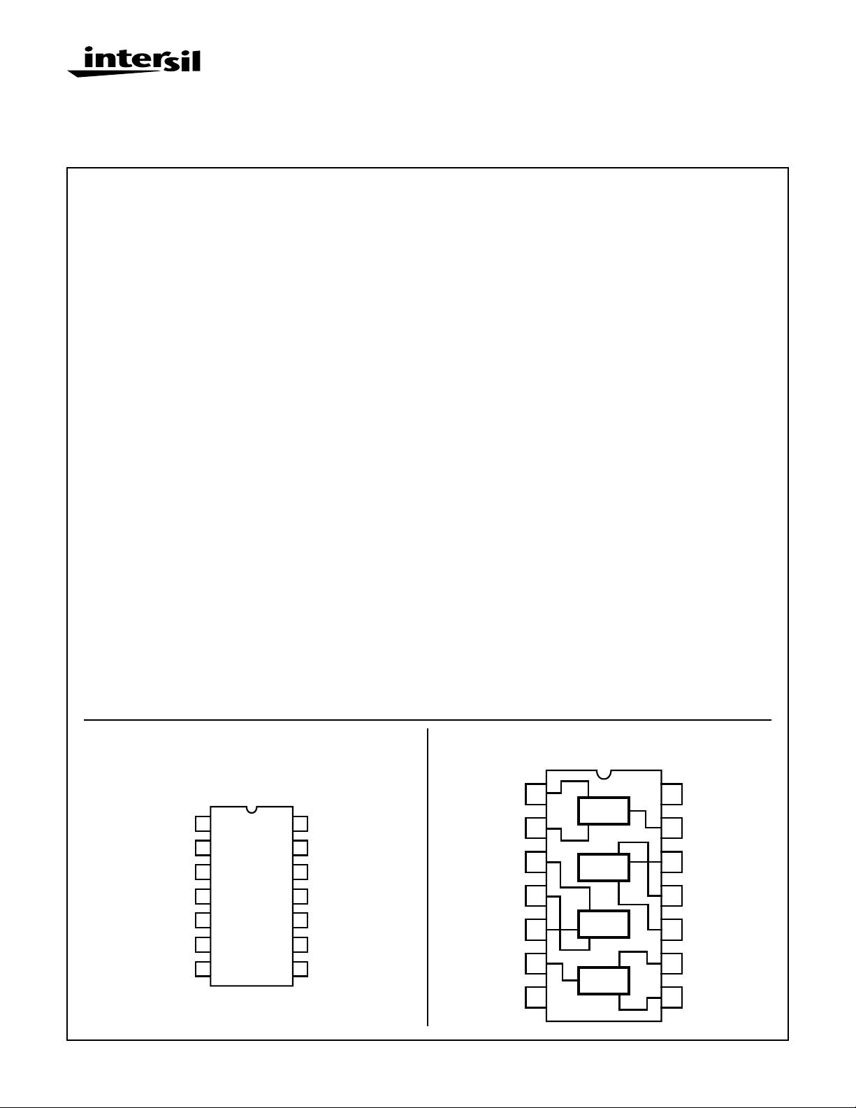
CD4016BMS Series types are quad bilateral switches intended
for the transmission or multiplexing of analog or digital signals.
Each of the four independent bilateral switches has a single control signal input which simultaneously biases both the p and n
device in a given switch on or off.
The CD4016BMS is supplied in these 14 lead outline packages:
Braze Seal DIP H4Q
o
C
Frit Seal DIP H1B
Ceramic Flatpack H3W
Pinout
CD4016BMS
TOP VIEW
SIG A IN
SIG A OUT
SIG B IN
SIG B OUT
CONTROL B
CONTROL C
CAUTION: These devices are sensitive to electrostatic discharge; follow proper IC Handling Procedures.
1-888-INTERSIL or 321-724-7143 | Copyright © Intersil Corporation 1999
VSS
1
2
3
4
5
6
7
VDD
14
CONTROL A
13
CONTROL D
12
SIG D IN
11
SIG D OUT
10
SIG C OUT
9
SIG C IN
8
Functional Diagram
IN/OUT
SIG A
OUT/IN
OUT/IN
SIG B
IN/OUT
CONTROL B
CONTROL C
VSS
7-733
1
2
3
4
5
6
7
SW
A
SW
D
SW
B
SW
C
14
VDD
13
CONTROL A
12
CONTROL D
11
IN/OUT
SIG D
10
OUT/IN
9
OUT/IN
SIG C
8
IN/OUT
File Number
3296

Specifications CD4016BMS
Absolute Maximum Ratings Reliability Information
DC Supply Voltage Range, (VDD) . . . . . . . . . . . . . . . -0.5V to +20V
(Voltage Referenced to VSS Terminals)
Input Voltage Range, All Inputs . . . . . . . . . . . . .-0.5V to VDD +0.5V
DC Input Current, Any One Input . . . . . . . . . . . . . . . . . . . . . . . .±10mA
Operating Temperature Range. . . . . . . . . . . . . . . . -55
Package Types D, F, K, H
Storage Temperature Range (TSTG). . . . . . . . . . . -65
o
C to +125oC
o
C to +150oC
Lead Temperature (During Soldering) . . . . . . . . . . . . . . . . . +265
At Distance 1/16 ± 1/32 Inch (1.59mm ± 0.79mm) from case for
10s Maximum
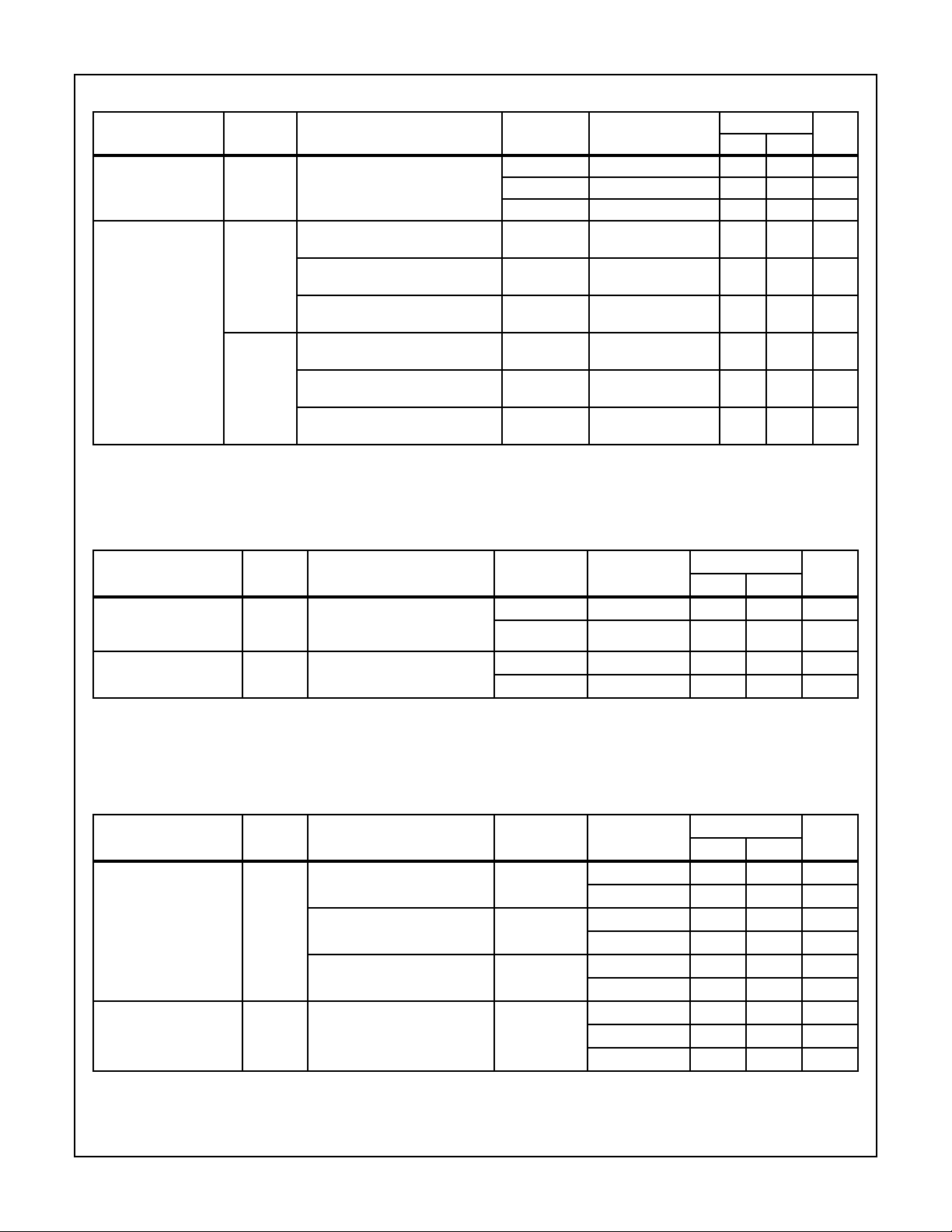
TABLE 1. DC ELECTRICAL PERFORMANCE CHARACTERISTICS
PARAMETER SYMBOL CONDITIONS (NOTE 1)
Supply Current IDD VDD = 20V, VIN = VDD or GND 1 +25
VDD = 18V, VIN = VDD or GND 3 -55oC - 0.5 µA
Input Leakage Current IIL VC = VDD or GND VDD = 20 1 +25
VDD = 18V 3 -55oC -100 - nA
Input Leakage Current IIH VC = VDD or GND VDD = 20 1 +25oC - 100 nA
VDD = 18V 3 -55oC - 100 nA
Input/Output Leakage
Current (Switch Off)
Input/Output Leakage
IOZL VDD = 18V, VC = 0V, VIS = 18V,
VOS = 0V
IOZH VDD = 18V, VIS = 18V, VOS = 0V 1 +25oC - 100 nA
Current (Switch Off)
N Threshold Voltage VNTH VDD = 10V, ISS = -10µA 1 +25oC -2.8 -0.7 V
P Threshold Voltage VPTH VSS = 0V, IDD = 10µA 1 +25oC 0.7 2.8 V
On-State Resistance
RON10 VIS = VDD or VSS, VDD = 10V 1 +25oC - 660 Ω
RL = 10K Returned to
VDD-VSS/2
RON10 VIS = 4.75V or 5.75V, VDD = 10V 1 +25oC - 2000 Ω
RON15 VIS = VDD or VSS, VDD = 15V 1 +25oC - 400 Ω
RON15 VIS = 7.25 or 7.75, VDD = 15V 1 +25oC - 850 Ω
Functional
(Note 3)
F VDD = 2.8V, VIN = VDD or GND 7 +25oC VOH >
VDD = 20V, VIN = VDD or GND 7 +25oC
VDD = 18V, VIN = VDD or GND 8A +125oC
VDD = 3V, VIN = VDD or GND 8B -55oC
Switch Threshold
RL = 100K to VDD
SWTHRH5 VDD = 5V, VC = 1.5V, VIS = GND 1, 2, 3 +25oC, +125oC, -55oC 4.1 - V
SWTHRH15 VDD = 15V, VC = 2V, VIS = GND 1, 2, 3 +25oC, +125oC, -55oC 14.1 - V
Thermal Resistance . . . . . . . . . . . . . . . . θ
Ceramic DIP and FRIT Package. . . . . 80oC/W 20oC/W
Flatpack Package . . . . . . . . . . . . . . . . 70
Maximum Package Power Dissipation (PD) at +125oC
For TA = -55
For TA = +100
o
C
Device Dissipation per Output Transistor . . . . . . . . . . . . . . . 100mW
o
C to +100oC (Package Type D, F, K). . . . . .500mW
o
C to +125oC (Package Type D, F, K) . . . . .Derate
Linearity at 12mW/oC to 200mW
ja
o
C/W 20oC/W
For TA = Full Package Temperature Range (All Package Types)
Junction Temperature . . . . . . . . . . . . . . . . . . . . . . . . . . . . . . +175oC
GROUP A
LIMITS
SUBGROUPS TEMPERATURE
o
C - 0.5 µA
2 +125
2 +125
o
C-50µA
o
C -100 - nA
o
C -1000 - nA
2 +125oC - 1000 nA
1 +25oC -100 - nA
2 +125oC -1000 - nA
3 -55oC -100 - nA
2 +125oC - 1000 nA
3 -55oC - 100 nA
2 +125oC - 960 Ω
3 -55oC - 600 Ω
2 +125oC - 2600 Ω
3 -55oC - 1870 Ω
2 +125oC - 600 Ω
3 -55oC - 360 Ω
2 +125oC - 1230 Ω
3 -55oC - 775 Ω
VOL <
VDD/2
VDD/2
θ
jc
UNITSMIN MAX
V
7-734

Specifications CD4016BMS
TABLE 1. DC ELECTRICAL PERFORMANCE CHARACTERISTICS (Continued)
GROUP A
PARAMETER SYMBOL CONDITIONS (NOTE 1)
Input Voltage Control,
Low (Note 2)
Control Input High
Voltage
(Note 2, Figure 12)
VIS = VSS, and
VIS = VDD
NOTES: 1. All voltages referenced to device GND, 100% testing being implemented.
2. Go/No Go test with limits applied to inputs
3. VDD = 2.8V/3V, RL = 100K to VDD
VDD = 20V/18V, RL = 10K to VDD
VILC VDD = 5V, VOS = VDD, VIS = VSS,
and VDD = 5V, VOS = VSS, VIS =
VDD, |IIS| < 10µA
VIHC VDD = 5V, |IIS| = .16mA, 4.6V <
VOS < 0.4V
VDD = 5V, |IIS| = .14mA, 4.6V <
VOS < 0.4V
VDD = 5V, |IIS| = .25mA, 4.6V <
VOS < 0.4V
VIHC VDD = 15V, |IIS| = 1.2mA, 13.5V <
VOS < 1.5V
VDD = 15V, |IIS| = 1.1mA, 13.5V <
VOS < 1.5V
VDD = 15V, |IIS| = 1.8mA, 13.5V <
VOS < 1.5V
SUBGROUPS TEMPERATURE
1 +25oC - 0.7 V
2 +125oC - 0.4 V
3 -55oC - 0.9 V
1 +25oC 3.5 - V
2 +125oC 3.5 - V
3 -55oC 3.5 - V
1 +25oC11-V
2 +125oC11-V
3 -55oC11-V
LIMITS
UNITSMIN MAX
TABLE 2. AC ELECTRICAL PERFORMANCE CHARACTERISTICS
GROUP A
PARAMETER SYMBOL CONDITIONS
Propagation Delay
Signal Input to Signal
Output
Propagation Delay
Turn On
NOTES:
1. CL = 50pF, RL = 200K, Input TR, TF < 20ns.
2. -55oC and +125oC limits guaranteed, 100% testing being implemented.
3. CL = 50pF, RL = 1K, TR, TF < 20ns.
PARAMETER SYMBOL CONDITIONS NOTES TEMPERATURE
Supply Current IDD VDD = 5V, VIN = VDD or GND 1, 2 -55oC, +25oC - 0.25 µA
Input Voltage Control,
Low
TPHL
TPLH
TPZH
TPZL
VILC VDD = 10V, VOS = VDD, VIS =
VDD = 5V, VIN = VDD or GND
(Notes 1, 2)
VDD = 5V, VIN = VDD or GND
(Notes 2, 3)
TABLE 3. ELECTRICAL PERFORMANCE CHARACTERISTICS
VDD = 10V, VIN = VDD or GND 1, 2 -55oC, +25oC - 0.5 µA
VDD = 15V, VIN = VDD or GND 1, 2 -55oC, +25oC - 0.5 µA
VSSand VOS = VSS, VIS = VDD
|IIS| < 10µA
SUBGROUPS TEMPERATURE
9 +25oC - 100 ns
10, 11 +125oC, -55oC - 135 ns
9 +25oC - 70 ns
10, 11 +125oC, -55oC - 95 ns
+125oC - 7.5 µA
+125oC-15µA
+125oC-30µA
1, 2 +25oC-55oC - 0.7 V
+125oC - 0.4 V
-55oC - 0.9 V
LIMITS
UNITSMIN MAX
LIMITS
UNITSMIN MAX
7-735
 Loading...