Intersil Corporation CD4011BT Datasheet

CD4011BT
Data Sheet July 1999 File Number
CMOS Quad 2-Input NAND Gate
Intersil’sSatellite Applications FlowTM(SAF) devices are fully
tested and guaranteed to 100kRAD total dose. These QML
Class T devices are processed to a standard flow intended
to meet the cost and shorter lead-time needs of large
volume satellite manufacturers, while maintaining a high
level of reliability.
The CD4011BT, Quad 2-Input NAND gate provides the
system designer with direct implementation of the NAND
function and supplements the existing family of CMOS
gates. All inputs and outputs are buffered.
Specifications
Specifications for Rad Hard QML devices are controlled by
the Defense Supply Center in Columbus (DSCC). The SMD
numbers listed below must be used when ordering.
Detailed Electrical Specifications for the CD4011BT are
contained in SMD 5962-96621. A “hot-link” is provided from
our website for downloading.
www.intersil.com/quality/manuals.asp
Intersil’s Quality Management Plan (QM Plan), listing all
Class T screening operations, is also available on our
website.
www.intersil.com/quality/manuals.asp
Ordering Information
4620.1
Features
• QML Class T, Per MIL-PRF-38535
• Radiation Performance
5
- Gamma Dose (γ) 1 x 10
- SEP Effective LET > 75 MEV/gm/cm
RAD(Si)
2
• Propagation Delay Time = 60ns (typ.) at CL = 50pF,
V
= 10V
DD
• Buffered Inputs and Outputs
• Standardized Symmetrical Output Characteristics
• 100% Tested for Maximum Quiescent Current at 20V
• 5V, 10V and 15V Parametric Ratings
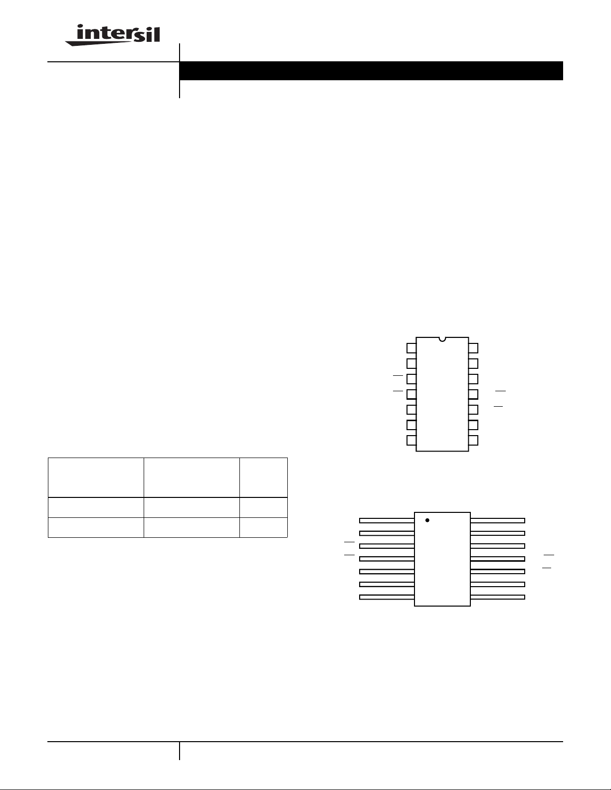
Pinouts
CD4011BT (SBDIP), CDIP2-T14
TOP VIEW
AB
J =
K = CD
V
SS
A
1
2
B
3
4
5
C
6
D
7
14
13
12
11
10
9
8
V
DD
H
G
M =
L = EF
E
F
GH
TEMP.
ORDERING
NUMBER
5962R9662101TCC CD4011BDTR -55 to 125
5962R9662101TXC CD4011BKTR -55 to 125
NOTE:
Minimumorderquantity for -T is 150 units through
PART
NUMBER
RANGE
(oC)
distribution, or 450 units direct.
1
CAUTION: These devices are sensitive to electrostatic discharge; follow proper IC Handling Procedures.
CD4011BT (FLATPACK), CDFP3-F14
TOP VIEW
1A
B
AB
J =
K =
CD
C
D
V
SS
www.intersil.com or 407-727-9207
2
3
4
5
6
7
14
13
12
11
10
9
8
| Copyright © Intersil Corporation 1999
V
H
G
M =
L =
E
F
DD
GH
EF

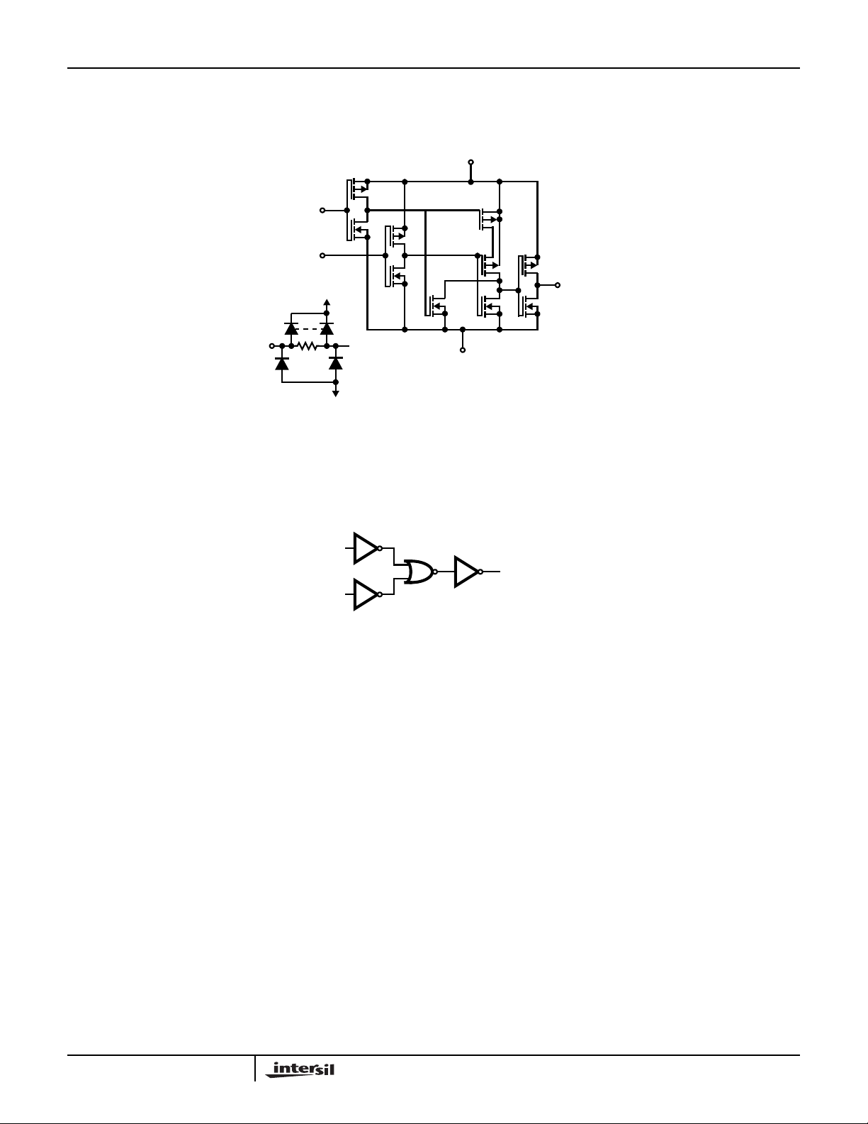
Schematic and Logic Diagram
CD4011BT
p
V
14
DD
1†
(8, 6, 13)
2†
(9, 5, 12)
V
SS
1(8, 6,13)
2(9, 5, 12)
n
p
n
V
DD
† ALL INPUTS ARE PROTECTED
BY CMOS PROTECTION NETWORK
n
1 OF 4 GATES (NUMBERS
IN PARENTHESES ARE
TERMINAL NUMBERS FOR
OTHER GATES)
LOGIC DIAGRAM
p
7V
SS
p
n
3
(10, 4, 11)
p
3 (10, 4, 11)
n
2
 Loading...