Intersil Corporation CD40106BMS Datasheet

CD40106BMS
December 1992
Features
• High Voltage Type (20V Rating)
• Schmitt Trigger Action with No External Components
• Hysteresis Voltage (Typ.)
- 0.9V at VDD = 5V
- 2.3V at VDD = 10V
- 3.5V at VDD = 15V
• Noise Immunity Greater than 50%
• No Limit on Input Rise and Fall Times
• Low VDD to VSS Current During Slow Input Ramp
• 100% Tested for Quiescent Current at 20V
• 5V, 10V and 15V Parametric Ratings
• Maximum Input Current of 1µA at 18V Over Full Pack-
age Temperature Range; 100nA at 18V and +25
• Standardized Symmetrical Output Characteristics
• Meets All Requirements of JEDEC Tentative Standard
No. 13B, “Standard Specifications for Description of
‘B’ Series CMOS Devices”
CMOS Hex Schmitt Triggers
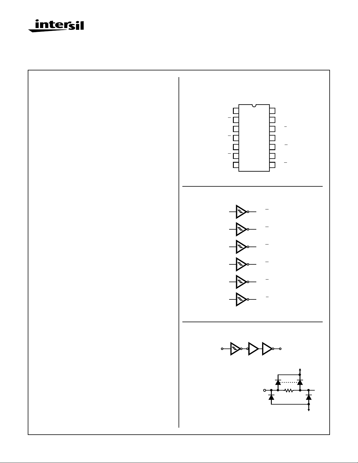
Pinout
CD40106BMS
TOP VIEW
A
1
A
2
G =
3
B
B
4
H =
5
C
C
6
I =
VSS
7
o
C
Functional Diagram
1
A
3
B
2
G =
4
H =
VDD
14
F
13
F
12
L =
11
E
E
10
K =
D
9
J =
D
8
A
B
Applications
• Wave and Pulse Shapers
• High Noise Environment Systems
• Monostable Multivibrators
• Astable Multivibrators
Description
CD40106BMS consists of six Schmitt trigger circuits. Each
circuit functions as an inverter with Schmitt trigger action on
the input. The trigger switches at different points for positive
and negative going signals. The difference between the
positive going voltage (VP) and the negative going voltage
(VN) is defined as hysteresis voltage (VH) (see Figure 17).
The CD40106BMS is supplied in these 14 lead outline
packages:
Braze Seal DIP H4Q
Frit Seal DIP H1B
Ceramic Flatpack H3W
C
D
E
F
Logic Diagram
*
1 (3, 5, 9, 11, 13)
ALL INPUTS ARE PROTECTED
*
BY CMOS PROTECTION
NETWORK
A
5
9
11
13
6
I =
C
8
J =
D
10
K =
E
12
L =
F
*
G
2 (4, 6, 8, 10, 12)
VDD
FIGURE 1. 1 OF 6 SCHMITT TRIGGERS
CAUTION: These devices are sensitive to electrostatic discharge; follow proper IC Handling Procedures.
1-888-INTERSIL or 321-724-7143 | Copyright © Intersil Corporation 1999
7-1327
File Number
VSS
3354

Specifications CD40106BMS
Absolute Maximum Ratings Reliability Information
DC Supply Voltage Range, (VDD) . . . . . . . . . . . . . . . -0.5V to +20V
(Voltage Referenced to VSS Terminals)
Input Voltage Range, All Inputs . . . . . . . . . . . . .-0.5V to VDD +0.5V
DC Input Current, Any One Input . . . . . . . . . . . . . . . . . . . . . . . .±10mA
Operating Temperature Range. . . . . . . . . . . . . . . . -55oC to +125oC
Package Types D, F, K, H
Storage Temperature Range (TSTG). . . . . . . . . . . -65oC to +150oC
Lead Temperature (During Soldering) . . . . . . . . . . . . . . . . . +265oC
At Distance 1/16 ± 1/32 Inch (1.59mm ± 0.79mm) from case for
10s Maximum
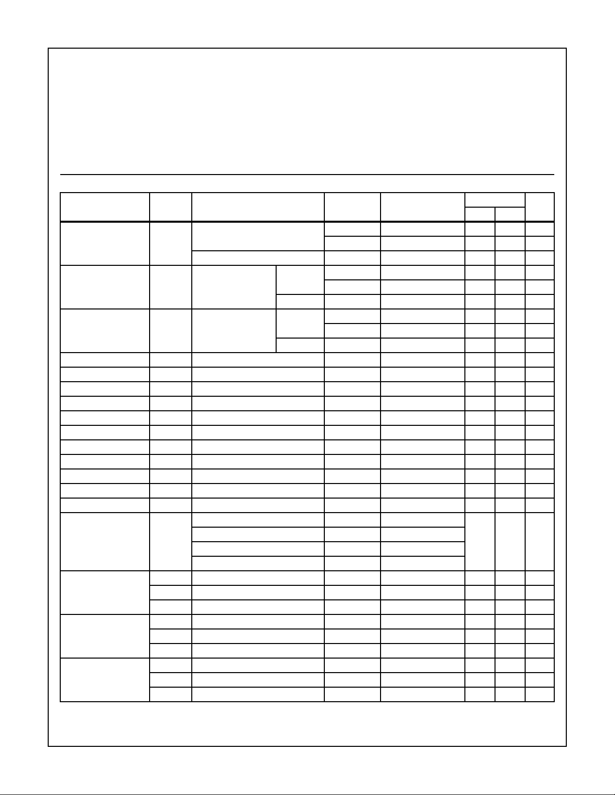
TABLE 1. DC ELECTRICAL PERFORMANCE CHARACTERISTICS
PARAMETER SYMBOL CONDITIONS (NOTE 1)
Supply Current IDD VDD = 20V, VIN = VDD or GND 1 +25oC-2µA
VDD = 18V, VIN = VDD or GND 3 -55oC-2µA
Input Leakage Current IIL VIN = VDD or GND VDD = 20 1 +25oC -100 - nA
VDD = 18V 3 -55oC -100 - nA
Input Leakage Current IIH VIN = VDD or GND VDD = 20 1 +25oC - 100 nA
VDD = 18V 3 -55oC - 100 nA
Output Voltage VOL15 VDD = 15V, No Load 1, 2, 3 +25oC, +125oC, -55oC - 50 mV
Output Voltage VOH15 VDD = 15V, No Load (Note 2) 1, 2, 3 +25oC, +125oC, -55oC 14.95 - V
Output Current (Sink) IOL5 VDD = 5V, VOUT = 0.4V 1 +25oC 0.53 - mA
Output Current (Sink) IOL10 VDD = 10V, VOUT = 0.5V 1 +25oC 1.4 - mA
Output Current (Sink) IOL15 VDD = 15V, VOUT = 1.5V 1 +25oC 3.5 - mA
Output Current (Source) IOH5A VDD = 5V, VOUT = 4.6V 1 +25oC - -0.53 mA
Output Current (Source) IOH5B VDD = 5V, VOUT = 2.5V 1 +25oC - -1.8 mA
Output Current (Source) IOH10 VDD = 10V, VOUT = 9.5V 1 +25oC - -1.4 mA
Output Current (Source) IOH15 VDD = 15V, VOUT = 13.5V 1 +25oC - -3.5 mA
N Threshold Voltage VNTH VDD = 10V, ISS = -10µA 1 +25oC -2.8 -0.7 V
P Threshold Voltage VPTH VSS = 0V, IDD = 10µA 1 +25oC 0.7 2.8 V
Functional F VDD = 2.8V, VIN = VDD or GND 7 +25oC VOH >
VDD = 20V, VIN = VDD or GND 7 +25oC
VDD = 18V, VIN = VDD or GND 8A +125oC
VDD = 3V, VIN = VDD or GND 8B -55oC
Positive Trigger
Threshold Voltage
(See Figure 17)
Negative Trigger
Threshold Voltage
(See Figure 17)
Hysteresis Voltage
(See Figure 17)
NOTES: 1. All voltages referenced to device GND, 100% testing being
implemented.
2. Go/No Go test with limits applied to inputs.
VP5 VDD = 5V 1, 2, 3 +25oC, +125oC, -55oC 2.2 3.6 V
VP10 VDD = 10V 1, 2, 3 +25oC, +125oC, -55oC 4.6 7.1 V
VP15 VDD = 15V 1, 2, 3 +25oC, +125oC, -55oC 6.8 10.8 V
VN5 VDD = 5V 1, 2, 3 +25oC, +125oC, -55oC 0.9 2.8 V
VN10 VDD = 10V 1, 2, 3 +25oC, +125oC, -55oC 2.5 5.2 V
VN15 VDD = 15V 1, 2, 3 +25oC, +125oC, -55oC 4 7.4 V
VH5 VDD = 5V 1, 2, 3 +25oC, +125oC, -55oC 0.3 1.6 V
VH10 VDD = 10V 1, 2, 3 +25oC, +125oC, -55oC 1.2 3.4 V
VH15 VDD = 15V 1, 2, 3 +25oC, +125oC, -55oC 1.6 5.0 V
Thermal Resistance . . . . . . . . . . . . . . . . θ
Ceramic DIP and FRIT Package. . . . . 80oC/W 20oC/W
Flatpack Package . . . . . . . . . . . . . . . . 70oC/W 20oC/W
Maximum Package Power Dissipation (PD) at +125oC
For TA = -55oC to +100oC (Package Type D, F, K) . . . . . .500mW
For TA = +100oC to +125oC (Package Type D, F, K). . . . . .Derate
Linearity at 12mW/oC to 200mW
Device Dissipation per Output Transistor . . . . . . . . . . . . . . . 100mW
For TA = Full Package Temperature Range (All Package Types)
Junction Temperature . . . . . . . . . . . . . . . . . . . . . . . . . . . . . . +175oC
GROUP A
SUBGROUPS TEMPERATURE
2 +125oC - 200 µA
2 +125oC -1000 - nA
2 +125oC - 1000 nA
3. For accuracy, voltage is measured differentially to VDD. Limit
is 0.050V max.
ja
LIMITS
VDD/2
VOL <
VDD/2
θ
jc
UNITSMIN MAX
V
7-1328

Specifications CD40106BMS
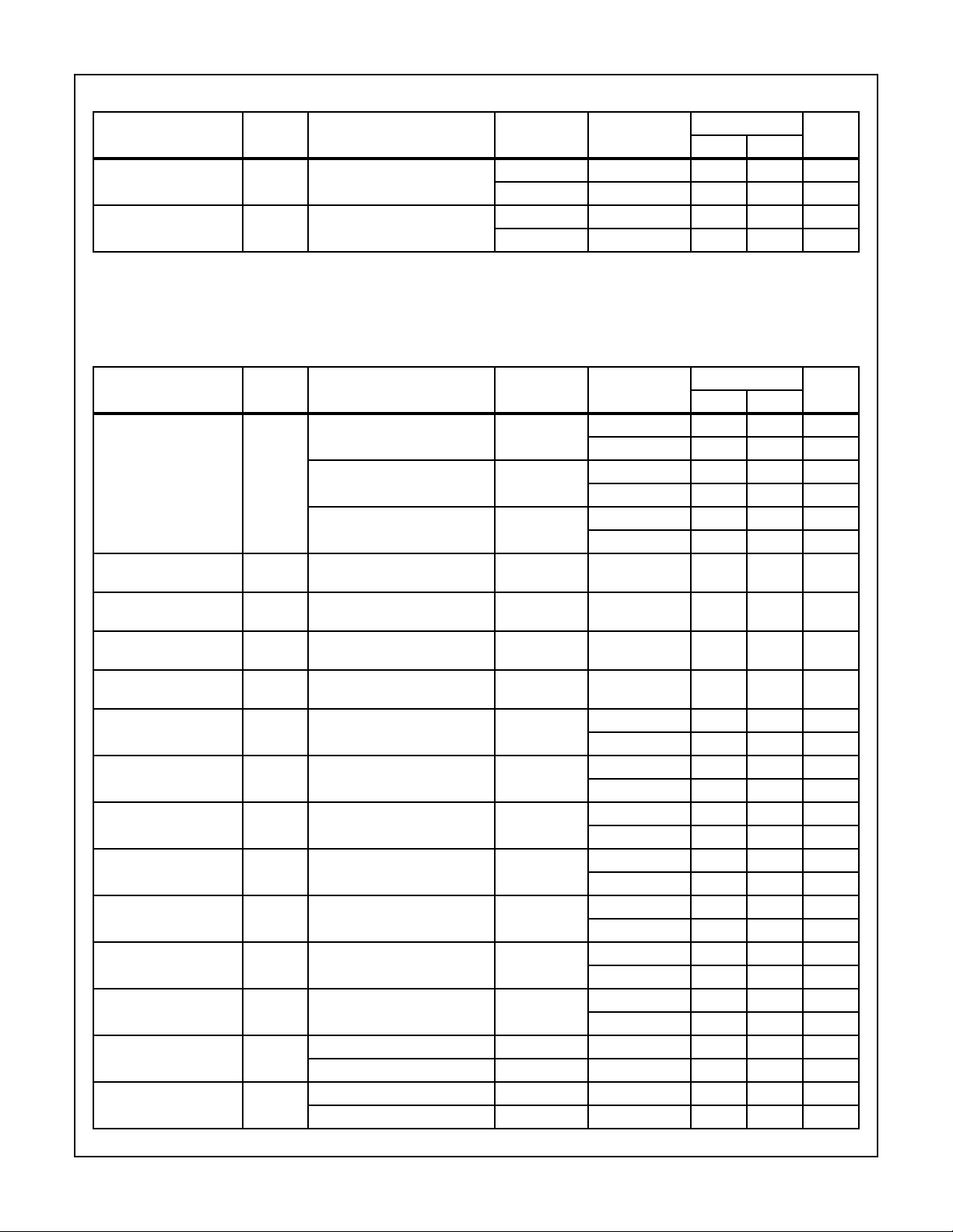
TABLE 2. AC ELECTRICAL PERFORMANCE CHARACTERISTICS
GROUP A
PARAMETER SYMBOL CONDITIONS (NOTE 1, 2)
Propagation Delay TPHL
TPLH
Transition Time TTHL
TTLH
NOTES:
1. CL = 50pF, RL = 200K, Input TR, TF < 20ns
2. -55oC and +125oC limits guaranteed, 100% testing being implemented.
PARAMETER SYMBOL CONDITIONS NOTES TEMPERATURE
Supply Current IDD VDD = 5V, VIN = VDD or GND 1, 2 -55oC, +25oC- 1 µA
Output Voltage VOL VDD = 5V, No Load 1, 2 +25oC, +125oC,
Output Voltage VOL VDD = 10V, No Load 1, 2 +25oC, +125oC,
Output Voltage VOH VDD = 5V, No Load 1, 2 +25oC, +125oC,
Output Voltage VOH VDD = 10V, No Load 1, 2 +25oC, +125oC,
Output Current (Sink) IOL5 VDD = 5V, VOUT = 0.4V 1, 2 +125oC 0.36 - mA
Output Current (Sink) IOL10 VDD = 10V, VOUT = 0.5V 1, 2 +125oC 0.9 - mA
Output Current (Sink) IOL15 VDD = 15V, VOUT = 1.5V 1, 2 +125oC 2.4 - mA
Output Current (Source) IOH5A VDD = 5V, VOUT = 4.6V 1, 2 +125oC - -0.36 mA
Output Current (Source) IOH5B VDD = 5V, VOUT = 2.5V 1, 2 +125oC - -1.15 mA
Output Current (Source) IOH10 VDD = 10V, VOUT = 9.5V 1, 2 +125oC - -0.9 mA
Output Current (Source) IOH15 VDD =15V, VOUT = 13.5V 1, 2 +125oC - -2.4 mA
Propagation Delay TPHL
TPLH
Transition Time TTHL
TTLH
VDD = 5V, VIN = VDD or GND 9 +25oC - 280 ns
VDD = 5V, VIN = VDD or GND 9 +25oC - 200 ns
TABLE 3. ELECTRICAL PERFORMANCE CHARACTERISTICS
VDD = 10V, VIN = VDD or GND 1, 2 -55oC, +25oC- 2 µA
VDD = 15V, VIN = VDD or GND 1, 2 -55oC, +25oC- 2 µA
VDD = 10V 1, 2, 3 +25oC - 140 ns
VDD = 15V 1, 2, 3 +25oC - 120 ns
VDD = 10V 1, 2, 3 +25oC - 100 ns
VDD = 15V 1, 2, 3 +25oC - 80 ns
SUBGROUPS TEMPERATURE
10, 11 +125oC, -55oC - 378 ns
10, 11 +125oC, -55oC - 270 ns
+125oC-30µA
+125oC-60µA
+125oC - 120 µA
-55oC
-55oC
-55oC
-55oC
-55oC 0.64 - mA
-55oC 1.6 - mA
-55oC 4.2 - mA
-55oC - -0.64 mA
-55oC - -2.0 mA
-55oC - -1.6 mA
-55oC - -4.2 mA
LIMITS
UNITSMIN MAX
LIMITS
UNITSMIN MAX
-50mV
-50mV
4.95 - V
9.95 - V
7-1329
 Loading...